Abstract
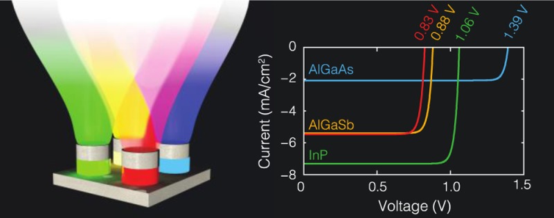
We present an approach to spectrum splitting for photovoltaics that utilizes the resonant optical properties of nanostructures for simultaneous voltage enhancement and spatial separation of different colors of light. Using metal–insulator–metal resonators commonly used in broadband metamaterial absorbers we show theoretically that output voltages can be enhanced significantly compared to single-junction devices. However, the approach is general and works for any type of resonator with a large absorption cross section. Due to its resonant nature, the spectrum splitting occurs within only a fraction of the wavelength, as opposed to traditional spectrum splitting methods, where many wavelengths are required. Combining nanophotonic spectrum splitting with other nanophotonic approaches to voltage enhancements, such as angle restriction and concentration, may lead to highly efficient but deeply subwavelength photovoltaic devices.
Keywords: photovoltaics, metasurfaces, plasmonics, critical coupling, detailed balance
The conversion efficiency of solar cells is an important factor in the cost per kWh, and improving it has therefore been a key goal of photovoltaic research. For a single-junction solar cell, such an efficiency enhancement can come from improving the current or voltage output, or both. Nanophotonic engineering has so far mostly been applied to solar cells with the goal of enhancing the absorption and thereby current of a thin semiconductor layer. This has been achieved using optical resonances in plasmonic1 or dielectric structures.2 By eliminating reflection and maximizing light trapping, such resonances can bring the solar cell short-circuit current (Jsc) close to that expected under the Shockley–Queisser limit.3 More recently, interest has shifted toward using nanophotonics to enhance the open-circuit voltage (Voc) of a solar cell.4 In general, this is achieved when the recombination rate is reduced with respect to the generation rate, resulting in higher carrier densities, which correspond to a larger Fermi-level splitting and thus higher output voltage.5 Nanophotonic modification of the recombination rate is possible via three different mechanisms: optical concentration, angle restriction, and optical band gap engineering. Optical concentration occurs when nanostructures act as antennas for light. This means that on resonance, nanostructures absorb photons from an area much larger than their physical cross section, leading to lower material consumption and thus lower bulk recombination rates without the need for focusing lenses or external optics.6,7 Alternatively, for cells that are dominated by radiative recombination, limiting the angles of emitted light through, for instance, a nanophotonic multilayer structure8,9 leads to photon recycling and as a result to higher carrier concentrations.
In addition to intrinsic optical concentration and angle restriction, nanophotonics can also be used to suppress absorption near a material’s electronic band gap to create an effective photonic band gap that is higher in energy.10−13 This works because due to reciprocity, reducing absorption near the band gap also makes it harder for carriers to recombine and emit a photon to the far field. Instead, photons are recycled in bulk cells,12 or the recombination rate is actually reduced due to changes in the local density of optical states (LDOS).13
Although this third approach increases the voltage output of the solar cell, the higher effective optical band gap also reduces the maximum current; it therefore cannot lead to a power conversion efficiency above the single-cell Shockley–Queisser (SQ) limit. The standard method to exceed this limit is to build a solar cell where materials with different band gaps are stacked on top of each other. This is the multijunction solar cell concept, where a top cell absorbs only high-energy photons, but transmits lower energy photons into the next layer (see Figure 1a). In each subcell the thermalization losses are small, so the overall conversion efficiency of photons is high. Efficiencies as high as 46% have been achieved using four different semiconductor layers that are grown on top of each other epitaxially.14 It has recently been shown theoretically that, with a two-layer multijunction architecture as in Figure 1a, the single-junction SQ can actually be surpassed even if both layers are made of the same material.15 This is achieved by increasing the voltage output of the top layer through photonic engineering, as described above.
Figure 1.

Diagrams depicting (a) the conventional tandem geometry, (b) a conventional spectrum splitting approach based on spectrally selective filters, and (c) nanophotonic spectrum splitting. In each case the contacting scheme is shown as well, with (a) a series connection, (b) each cell connected independently, and (c) a four-terminal connection with a shared positive contact.
Although multijunction solar cells are a proven concept for high efficiencies, their design and fabricaiton is complicated. Since the standard multijunction solar cell is grown epitaxially, each layer has to be lattice matched and produce the same current (which puts constraints on the band gap). The difficulty involved in finding the ideal combination of band gaps and lattice constants makes spectrum splitting multijunctions—where the subcells are not placed on top of each other but next to each other—quite appealing (see Figure 1b).16−18 This spectral splitting is typically done on macroscopic length scales using external optics, such as dichroic mirrors.
Just as focusing optics can be replaced by nanoscale resonances to provide optical concentration (as described above), nanostructures also provide an opportunity for spectrum splitting without external macroscopic optics. In this Letter we propose such an alternative approach to spectrum splitting, where the resonant optical properties of nanoparticles are responsible for both the voltage enhancement (due to an increased optical band gap) and the actual spectrum splitting (see Figure 1c). This approach is based on the fact that nanoparticles can have very large absorption cross sections and that sufficiently detuned resonators operate independently, even if they are closely spaced. As opposed to the approaches in Figure 1a and b, where colors are separated over distances of many wavelengths, nanophotonic spectrum splitting occurs within a fraction of the wavelength. As a result, the multijunction solar cell can have a subwavelength height, significantly reducing material consumption.
We begin by investigating an array of identical resonant particles, to gauge the voltage enhancements that can be achieved through nanophotonic manipulation of the band gap alone. We will then move on to an array of detuned resonators in one unit cell, to investigate nanophotonic spectrum splitting. Since the resonators are spatially separated, we are not restricted to certain materials or lattice constants. Hence, we will also look at nanophotonic spectrum splitting when resonators are made from different semiconductors. Although in this study we investigate metal–insulator–metal patch resonators, the results are general and apply to any nanostructured resonator with a large absorption cross section. We believe that this approach to spectrum splitting facilitates further integration with other nanophotonic concepts for voltage enhancements such as angle restriction8,9 and, in the presence of nonradiative recombination, concentration.6,7
Nanostructures, particularly at resonance, can have an absorption cross section (Cabs) that is much larger than their geometrical cross section (Cgeo):19
| 1 |
where Qabs is called the absorption efficiency. As a result, an array of identical nanostructures with large spacing in between can still absorb all of the incident light at the resonance wavelength.20,21 An example of such an array is depicted in Figure 2a, where a small metal–insulator–metal (MIM) resonator is shown in a 400 by 400 nm unit cell. The MIM configuration supports so-called MIM waveguide modes, which reflect off the sides of the disk and form a Fabry–Perot-like resonance.22−24 In our case the metal substrate and top hat are silver (Ag) and in between is a disk of aluminum gallium arsenide (Al0.3Ga0.7Sb). Using finite-difference time-domain (Lumerical FDTD) we calculated the absorption in the semiconductor under normal incidence illumination for a range of wavelengths and MIM disk diameters (Figure 2b; see Figure S1 for full spectrum and total absorptance including in silver). A strong absorption peak corresponding to the fundamental MIM resonance is shown red-shifting and increasing in intensity for larger diameters, until the peak amplitude starts to decrease close to the band gap (1130 nm/1.1 eV25). This variation in amplitude is due to changes in the absorption loss rate of the resonance, which depends on the extinction coefficient of Al0.3Ga0.7Sb. Resonances absorb most strongly when their radiative loss rate and absorption loss rate are equal (the so-called critical coupling condition), and an increase or decrease in the absorption loss rate reduces the peak amplitude.26 The radiative loss rate of the MIM resonator is low (its bandwidth is small), so counterintuitively it absorbs most when the extinction coefficient is also low (close to the band gap).
Figure 2.
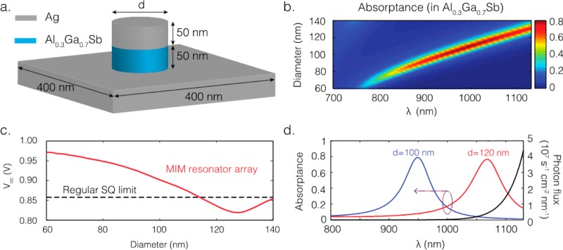
(a) Diagram of the MIM resonator array with a unit cell size of 400 by 400 nm. (b) Absorption spectrum of a periodic array of identical MIM resonators, for different diameters d (see a). (c) Voc of the MIM array (red), compared to the Shockley–Queisser Voc for a perfectly absorbing solar cell (dashed black) with the same band gap. (d) Absorption spectrum of the MIM array for two diameters and the blackbody spectrum at 300 K for unity emissivity in black.
If the absorptivity of a geometry such as an array of nanostructures is known over the whole range of the solar spectrum and all angles, one can calculate the maximum open-circuit voltage (Voc) using the detailed balance framework:11
| 2 |
where q is the electron charge, kB is the Boltzmann constant, T is the temperature of the solar cell, and Jsc and J0 are the short-circuit and reverse saturation current density, respectively. The Jsc is obtained simply by integrating the semiconductor absorptance of the array under normal incidence and over the solar spectrum (i.e., assuming 100% internal quantum efficiency), while calculation of J0 is a little more involved. In the dark a very small amount of carriers are generated because of above band gap blackbody radiation, and in equilibrium the same amount of carriers must recombine (the principle of detailed balance).3,11J0 can thus be found by integrating the full hemisphere absorption spectrum over the blackbody spectrum at ambient temperatures. This gives for Jsc and J0
| 3a |
| 3b |
Here S(ω) is the AM1.5 solar spectrum,27 and ψa is the blackbody spectrum at ambient temperatures (Ta = 300 K). A(ω,θ,ϕ) is the unpolarized absorbtance of the total array in the semiconductor, thus excluding absorption in silver, as a function of incident angle. In eq 3b the cos(θ) term is due to Lambert’s cosine rule, and the sin(θ) term accounts for the solid angle. We have assumed that the illumination occurs only at normal incidence (eq 3a), which is a good approximation considering the small solid angle occupied by the sun, while for recombination we integrate over the full hemisphere (eq 3b). Furthermore, we have assumed that there is only radiative recombination to the far-field. Finally, we have assumed that the absorption is in fact isotropic (A(ω,θ,ϕ) = A(ω)), which is a good assumption because, due to the subwavelength lattice, the response is based on the single MIM resonator28 (see Supporting Information Figure S4).
The Voc of this array, shown in red in Figure 2c, varies with diameters and for small diameters is significantly higher than the regular Shockley–Queisser Voc (dashed black line). As the absorptance is isotropic, this voltage enhancement is not due to angle restriction effects (see Supporting Information), but instead the origin lies in the suppression of absorption near the band gap.10−13 As thermal emission peaks near the band gap and then decays exponentially for higher energies, moving a resonance to shorter wavelengths reduces J0 dramatically. For example, Figure 2d shows the absorption spectra of 100 and 120 nm diameter MIM resonator arrays together with the 300 K blackbody spectrum. Because the integrated product of the 100 nm disk absorption and the blackbody spectrum is much smaller, the equilibrium thermal emission is lower and the Voc is increased.
Although voltages are enhanced significantly, the absorption bandwidth is small and, as a result, so is the current. However, because Qabs is large enough, this can leave ample room to interdigitate a second (or third, fourth, etc.) array detuned from the first to absorb strongly at another wavelength. This is the basic principle of some broadband metamaterial absorbers, where it is used to enhance the absorbing bandwidth of an array.21,24,28−30 Since at different wavelengths light is absorbed in physically different positions, this phenomenon has also been suggested for photon sorting.29,31 Photon sorting is exactly what is required in a multijunction solar cell, where photons are directed to and absorbed in a subcell where they are converted most efficiently. We can thus use the resonant properties of these nanoscale resonators to simultaneously enhance the voltage and split the spectrum.
To achieve nanophotonic spectrum splitting, we place multiple detuned resonators in the same subwavelength unit cell (see Figure 3a). The absorption spectrum of the array is shown in Figure 3b, with, in solid black, the total absorption and, in colors, the different semiconductor disks. The spectra over the whole solar range for both polarizations are shown in Figure S2.
Figure 3.
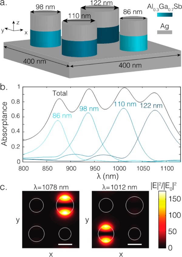
(a) Diagram of the MIM resonator array, now with four resonators in a unit cell. They are positioned equally far from each other (200 nm spacing between centers). (b) Absorption spectrum of this array, where black is total absorption and shades of blue are the different size resonators individually, excluding absorption in the silver. (c) Field enhancement plots showing the electric field density at different wavelengths corresponding to the resonant frequencies of the different resonators. The scale bar is 100 nm. The plot depicts the 400 by 400 nm xy-plane in the middle of the semiconductor cylinder (z = 25 nm above the Ag substrate). Polarization is along the y-axis in both b and c (other polarization in Figure S2).
The absorption spectrum shows that this geometry spatially separates colors: at different wavelengths absorption peaks in different resonators (total absorption reaches over 90% in three out of four resonators), which are physically separated, without the need for external optics. This is even more clearly visible in Figure 3c, where the electric field intensity enhancement |E|2/|E0|2 is shown (E0 is the incident field amplitude). The two plots correspond to the peak wavelengths of the two larger resonators in Figure 3b. At the different wavelengths high-field intensities are visible in the resonant nanostructures while the off-resonance nanostructures remain dark, which visualizes how light is captured and the spectrum is split by the resonators.
Using eq 2 we can calculate the open-circuit voltage and short circuit from each resonator in the array. We can then calculate the J–V curve corresponding to each resonator, which is given by the ideal diode equation (J(V) = Jsc – J0 exp(qV/kBT)3,11). From these curves, shown in Figure 4, it is clear that again the Voc for each resonator has increased: 825, 880, 905, and 937 mV for the largest to smallest resonators, respectively. This remarkable increase of more than 100 mV in the Voc (14%) using exactly the same material arises only through careful engineering of the nanophotonic resonances. The current of each resonator is relatively small due to the narrow bandwidth, as mentioned above, which limits the efficiency. Although in the current design this limits the total power conversion efficiency to 13.91%, we can show that spectrum splitting does actually improve the efficiency of the array by making two comparisons. First of all, if each resonator in the array has the same size, the efficiency would be comparable to the single resonator array discussed before. Due to significantly lower currents, this efficiency is below 6% (see Supporting Information). Second, we can compare it to a configuration where all resonators are connected in parallel. In that case the voltage over each cell is equal, and the advantage of spectrum splitting is lost. For the device in Figure 3a this leads to an efficiency of 13.41%, so spectrum splitting has led to an increase in efficiency of almost 4%.
Figure 4.
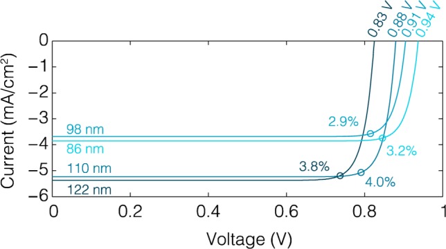
Current–voltage curves for the separate AlGaSb resonators in Figure 3a.
Although we have demonstrated that nanophotonic spectrum splitting can lead to a multijunction solar cell using only a single material by proper resonance engineering, the improvement in efficiency is still modest (4%). Further gains in Voc are possible by making the different resonators from materials with different band gaps. Figure 5a shows a unit cell with two detuned Al0.3Ga0.7Sb resonators (band gap = 1.1 eV), one indium phosphide (InP, band gap = 1.34 eV25), and one aluminum gallium arsenide (Al0.2Ga0.8As, band gap = 1.67 eV25) resonator. The absorption spectrum of the array is shown in Figure 5b, with absorption in each semiconductor disk shown as a colored curve. Figure 5c shows the J–V curves of the different resonators, and we immediately notice that higher Voc values are indeed achieved: the AlGaAs subcell has a Voc of 1.39 V and the InP subcell has a Voc of about 1.06 V. This enhanced voltage compared to the AlGaSb resonators is due to the fact that the AlGaAs and InP resonators naturally do not absorb at all below their band gap, leading to a lower J0. This increase in output voltage positively affects the efficiency: it has increased by 27% from 13.91% for the AlGaSb array to 17.53%, while the total Jsc has increased by only 12% to 20.3 mA/cm2. As with the AlGaSb array, the efficiency is still limited by the generated current, due to the narrow-bandwidth resonators. To increase the efficiency, the current has to be increased by either including more resonators or using resonators with a larger bandwidth. Ideally one would increase the number of narrow-band resonators to keep thermalization losses as low as possible, but it may be more practical to use larger bandwidth resonances or a nanostructure that supports multiple resonances in the same frequency window.26,32 Additionally, although current enhancements in plasmonic metal–semconductor systems have been observed experimentally,33,34 the presence of metal might lead to a reduction of the internal quantum efficiency due to, for example, quenching of carriers. Purely dielectric nanophotonic structures might therefore be more favorable to achieve high internal quantum efficiencies and to avoid ohmic absorption losses.
Figure 5.
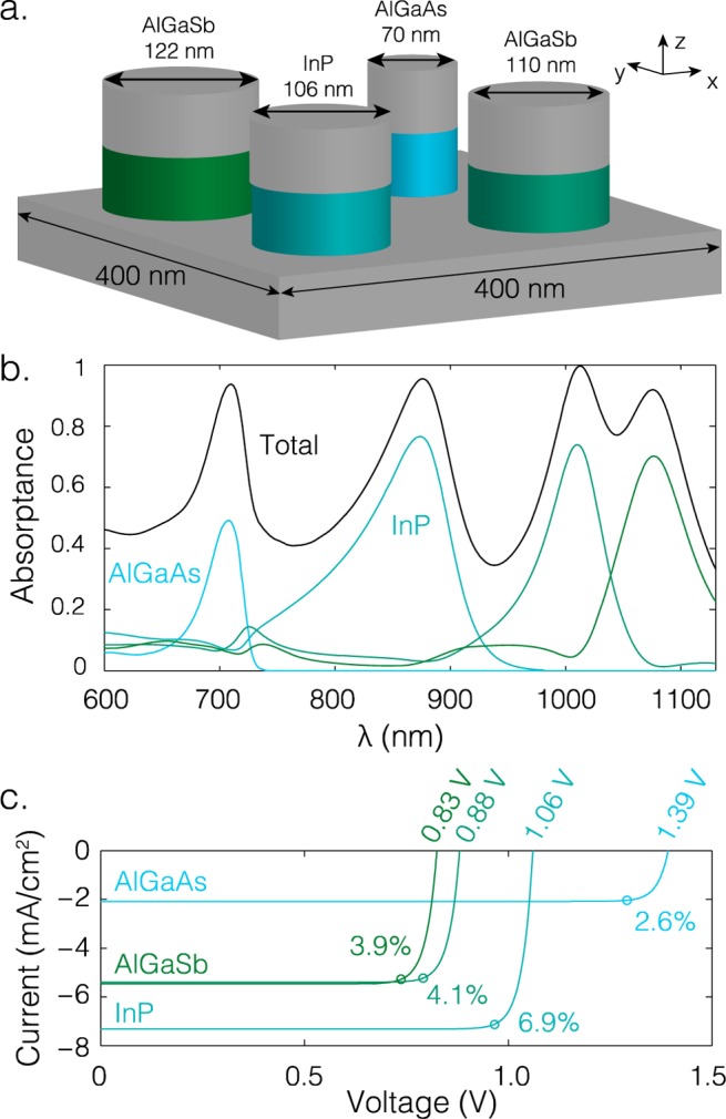
(a) Diagram of the MIM resonator array, now with four resonators in a unit cell. Two resonators comprise AlGaSb as an absorber, one InP and one AlGaAs. They are positioned equally far from each other (200 nm spacing between centers). (b) Absorption spectrum of this array, where black is total absorption and the colored curves show absorption in the semiconductor material of the individual resonators, excluding absorption in the silver (unmarked curves correspond to the AlGaSb pair). Polarization is along the y-axis; see Figure S3 for other polarization. (c) Current–voltage curves for the four independent resonators in part a.
To conclude, we have investigated theoretically spectrum splitting for photovoltaic applications utilizing arrays of nanoscale antennas with different resonant frequencies. This allows for simultaneous voltage enhancement and spatial separation of different colors of light. Such an intrinsic spectrum-splitting mechanism relaxes the lattice and current-matching requirements compared to the typical multijunction solar cells, while also eliminating the need for external splitting optics. Additionally, this was achieved in an array with a deeply subwavelength height. Efficiency enhancements are observed for a multijunction spectrum-splitting design that uses only a single semiconductor due to suppression of absorption near the band gap in some of the resonators, which leads to higher voltages. Much larger efficiency enhancements are observed when the different resonators are made from different semiconductors, due to the more stringent reduction of reverse saturation currents that comes with increasing electronic band gaps. The nanophotonic spectrum-splitting and voltage enhancement approach presented here is general for any type of nanoscale resonator, dielectric or plasmonic, and efficiencies can be enhanced significantly by using larger bandwidth resonances while still maintaining high optical cross sections. Combining nanophotonic spectrum splitting with other nanophotonic approaches to voltage enhancements, such as angle restriction and concentration, may lead to deeply subwavelength, yet highly efficient photovoltaic devices with very low material consumption.
Acknowledgments
We gratefully acknowledge Prof. Andrea Alù for discussions and a thorough reading of the manuscript and Ricardo Struik for the Table of Contents schematic. This work is part of the research program of the Foundation for Fundamental Research on Matter (FOM), which is part of The Netherlands Organisation for Scientific Research (NWO).
Supporting Information Available
Full absorption spectra of the arrays considered in the main text, for both polarizations; short-circuit current and efficiency for the single resonator array in Figure 2; absorption as a function of angle; simulation details. The Supporting Information is available free of charge on the ACS Publications website at DOI: 10.1021/acsphotonics.5b00260.
The authors declare no competing financial interest.
Supplementary Material
References
- Atwater H. A.; Polman A. Plasmonics for Improved Photovoltaic Devices. Nat. Mater. 2010, 9, 205–213 10.1038/nmat2629. [DOI] [PubMed] [Google Scholar]
- Brongersma M. L.; Cui Y.; Fan S. Light Management for Photovoltaics Using High-Index Nanostructures. Nat. Mater. 2014, 13, 451–460 10.1038/nmat3921. [DOI] [PubMed] [Google Scholar]
- Shockley W.; Queisser H. J. Detailed Balance Limit of Efficiency of P-N Junction Solar Cells. J. Appl. Phys. 1961, 32, 510–519 10.1063/1.1736034. [DOI] [Google Scholar]
- Polman A.; Atwater H. A. Photonic Design Principles for Ultrahigh-Efficiency Photovoltaics. Nat. Mater. 2012, 11, 174–177 10.1038/nmat3263. [DOI] [PubMed] [Google Scholar]
- Wurfel P. The Chemical Potential of Radiation. J. Phys. C: Solid State Phys. 1982, 15, 3967–3985 10.1088/0022-3719/15/18/012. [DOI] [Google Scholar]
- Krogstrup P.; Jørgensen H. I.; Heiss M.; Demichel O.; Holm J. V.; Aagesen M.; Nygard J.; Fontcuberta i Morral A. Single-Nanowire Solar Cells beyond the Shockley–Queisser Limit. Nat. Photonics 2013, 7, 1–5 10.1038/nphoton.2013.32. [DOI] [Google Scholar]
- Wallentin J.; Anttu N.; Asoli D.; Huffman M.; Aberg I.; Magnusson M. H.; Siefer G.; Fuss-Kailuweit P.; Dimroth F.; Witzigmann B.; Xu H. Q.; Samuelson L.; Deppert K.; Borgström M. T. InP Nanowire Array Solar Cells Achieving 13.8% Efficiency by Exceeding the Ray Optics Limit. Science 2013, 339, 1057–1060 10.1126/science.1230969. [DOI] [PubMed] [Google Scholar]
- Kosten E. D.; Atwater J. H.; Parsons J.; Polman A.; Atwater H. A.. Highly Efficient GaAs Solar Cells by Limiting Light Emission Angle. Light: Sci. Appl. 2013, 2.e45. 10.1038/lsa.2013.1 [DOI] [Google Scholar]
- Kosten E. D.; Kayes B. M.; Atwater H. A. Experimental Demonstration of Enhanced Photon Recycling in Angle-Restricted GaAs Solar Cells. Energy Environ. Sci. 2014, 7, 1907–1912 10.1039/c3ee43584a. [DOI] [Google Scholar]
- Sandhu S.; Yu Z.; Fan S. Detailed Balance Analysis and Enhancement of Open-Circuit Voltage in Single-Nanowire Solar Cells. Nano Lett. 2014, 14, 1011–1015 10.1021/nl404501w. [DOI] [PubMed] [Google Scholar]
- Sandhu S.; Yu Z.; Fan S. Detailed Balance Analysis of Nanophotonic Solar Cells. Opt. Express 2013, 21, 1209–1217 10.1364/OE.21.001209. [DOI] [PubMed] [Google Scholar]
- Munday J. N. The Effect of Photonic Bandgap Materials on the Shockley-Queisser Limit. J. Appl. Phys. 2012, 112, 064501. 10.1063/1.4742983. [DOI] [Google Scholar]
- Niv A.; Gharghi M.; Gladden C.; Miller O. D.; Zhang X. Near-Field Electromagnetic Theory for Thin Solar Cells. Phys. Rev. Lett. 2012, 109, 138701 1–5 10.1103/PhysRevLett.109.138701. [DOI] [PubMed] [Google Scholar]
- Green M. A.; Emery K.; Hishikawa Y.; Warta W.; Dunlop E. D. Solar Cell Efficiency Tables (Version 46). Prog. Photovoltaics 2015, 23, 805–812 10.1002/pip.2573. [DOI] [Google Scholar]
- Yu Z.; Sandhu S.; Fan S. Efficiency above the Shockley–Queisser Limit by Using Nanophotonic Effects To Create Multiple Effective Bandgaps with a Single Semiconductor. Nano Lett. 2014, 14, 66–70 10.1021/nl403653j. [DOI] [PubMed] [Google Scholar]
- Imenes A. G.; Mills D. R. Spectral Beam Splitting Technology for Increased Conversion Efficiency in Solar Concentrating Systems: A Review. Sol. Energy Mater. Sol. Cells 2004, 84, 19–69 10.1016/j.solmat.2004.01.038. [DOI] [Google Scholar]
- Eisler C. N.; Abrams Z. R.; Sheldon M. T.; Zhang X.; Atwater H. A. Multijunction Solar Cell Efficiencies: Effect of Spectral Window, Optical Environment and Radiative Coupling. Energy Environ. Sci. 2014, 7, 3600–3605 10.1039/C4EE01060D. [DOI] [Google Scholar]
- Green M. A.; Ho-Baillie A. Forty Three per Cent Composite Split-Spectrum Concentrator Solar Cell Efficiency. Prog. Photovoltaics 2010, 18, 42–47 10.1002/pip.924. [DOI] [Google Scholar]
- Bohren C. E.; Huffman D. R.. Absorption and Scattering of Light by Small Particles; Wiley-VCH, 1984. [Google Scholar]
- Ra’di Y.; Simovski C. R.; Tretyakov S. A. Thin Perfect Absorbers for Electromagnetic Waves: Theory, Design, and Realizations. Phys. Rev. Appl. 2015, 3, 1–37 10.1103/PhysRevApplied.3.037001. [DOI] [Google Scholar]
- Cui Y.; He Y.; Jin Y.; Ding F.; Yang L.; Ye Y.; Zhong S.; Lin Y.; He S. Plasmonic and Metamaterial Structures as Electromagnetic Absorbers. Laser Photon. Rev. 2014, 8, 495–520 10.1002/lpor.201400026. [DOI] [Google Scholar]
- Yang J.; Sauvan C.; Jouanin A.; Collin S.; Pelouard J.; Lalanne P. Ultrasmall Metal-Insulator-Metal Nanoresonators: Impact of Slow-Wave Effects on the Quality Factor. Opt. Express 2012, 20, 738–743 10.1364/OE.20.016880. [DOI] [Google Scholar]
- Chandran A.; Barnard E. S.; White J. S.; Brongersma M. L. Metal-Dielectric-Metal Surface Plasmon-Polariton Resonators. Phys. Rev. B: Condens. Matter Mater. Phys. 2012, 85, 085416. 10.1103/PhysRevB.85.085416. [DOI] [Google Scholar]
- Koechlin C.; Bouchon P.; Pardo F.; Pelouard J.; Haidar R. Analytical Description of Subwavelength Plasmonic MIM Resonators and of Their Combination. Opt. Express 2013, 21, 4641–4647 10.1364/OE.21.007025. [DOI] [PubMed] [Google Scholar]
- Adachi S.Properties of Semiconductor Alloys: Group-IV, III–V and II–VI Semiconductors; John Wiley & Sons, Ltd., 2009. [Google Scholar]
- Mann S. A.; Garnett E. C. Extreme Light Absorption in Thin Semiconducting Films Wrapped around Metal Nanowires. Nano Lett. 2013, 13, 1–9 10.1021/nl401179h. [DOI] [PubMed] [Google Scholar]
- National Renewable Energy Lab (NREL). Air Mass 1.5 (AM1.5) Global Spectrum (ASTM173-03G), http://rredc.nrel.gov/solar/spectra/am1.5/, 2008.
- Cheng C.-W.; Abbas M. N.; Chiu C.-W.; Lai K.-T.; Shih M.-H.; Chang Y.-C. Wide-Angle Polarization Independent Infrared Broadband Absorbers Based on Metallic Multi-Sized Disk Arrays. Opt. Express 2012, 20, 10376–10381 10.1364/OE.20.010376. [DOI] [PubMed] [Google Scholar]
- Le Perchec J.; Desieres Y.; Rochat N.; Espiau de Lamaestre R. Subwavelength Optical Absorber with an Integrated Photon Sorter. Appl. Phys. Lett. 2012, 100, 113305. 10.1063/1.3694749. [DOI] [Google Scholar]
- Nielsen M. G.; Pors A.; Albrektsen O.; Bozhevolnyi S. I. Efficient Absorption of Visible Radiation by Gap Plasmon Resonators. Opt. Express 2012, 20, 13311–13319 10.1364/OE.20.013311. [DOI] [PubMed] [Google Scholar]
- Koechlin C.; Bouchon P.; Pardo F.; Jaeck J.; Lafosse X.; Pelouard J. L.; Haïdar R. Total Routing and Absorption of Photons in Dual Color Plasmonic Antennas. Appl. Phys. Lett. 2011, 99, 38–41 10.1063/1.3670051. [DOI] [Google Scholar]
- Mohammadi Estakhri N.; Alù A. Minimum-Scattering Superabsorbers. Phys. Rev. B: Condens. Matter Mater. Phys. 2014, 89, 121416. 10.1103/PhysRevB.89.121416. [DOI] [Google Scholar]
- Fan P.; Huang K. C. Y.; Cao L.; Brongersma M. L. Redesigning Photodetector Electrodes as an Optical Antenna. Nano Lett. 2013, 13, 392–396 10.1021/nl303535s. [DOI] [PubMed] [Google Scholar]
- Brittman S.; Gao H.; Garnett E. C.; Yang P. Absorption of Light in a Single-Nanowire Silicon Solar Cell Decorated with an Octahedral Silver Nanocrystal. Nano Lett. 2011, 11, 5189–5195 10.1021/nl2023806. [DOI] [PubMed] [Google Scholar]
Associated Data
This section collects any data citations, data availability statements, or supplementary materials included in this article.


