Abstract
We demonstrate a method to fabricate graphene microelectrode arrays (MEAs) using a simple and inexpensive method to solve the problem of opaque electrode positions in traditional MEAs, while keeping good biocompatibility. To study the interface differences between graphene–electrolyte and gold–electrolyte, graphene and gold electrodes with a large area were fabricated. According to the simulation results of electrochemical impedances, the gold–electrolyte interface can be described as a classical double-layer structure, while the graphene–electrolyte interface can be explained by a modified double-layer theory. Furthermore, using graphene MEAs, we detected the neural activities of neurons dissociated from Wistar rats (embryonic day 18). The signal-to-noise ratio of the detected signal was 10.31 ± 1.2, which is comparable to those of MEAs made with other materials. The long-term stability of the MEAs is demonstrated by comparing differences in Bode diagrams taken before and after cell culturing.
Keywords: Microelectrode arrays, MEA, Graphene, Neural activity detection
Introduction
Microelectrode arrays (MEAs) are useful tools for studying electrogenic cells [1]. Compared with patch clamps, MEAs are able to facilitate the long-term observation of cell electrical activity without damaging the cells. Additionally, MEAs can detect electric signals from cells at multiple points and also have the ability to supply electric stimulus simultaneously. This enables neuronal networks to be studied, which have complex structures. Numerous materials, including titanium nitride [2] and titanium [3], have been used in the fabrication of MEAs. However, these traditional materials are not transparent. Indium tin oxide (ITO) electrodes have partially solved this problem but they still need a non-transparent metal layer at the electrode sites because bare ITO electrodes can be etched, causing the recorded action potential to have a low signal-to-noise ratio (SNR) [4], which would interrupt the observation of the cells.
Graphene, a two-dimensional single-atom-thick carbon lattice, is one of the most promising materials that has high conductance and high mechanical strength as well as biocompatibility [5]. Recently, graphene has been used to fabricate transistors, demonstrating its great potential in detecting action potentials [6, 7]. However, the intrinsic noise in transistors limits their sensitivity. Currently, the effective gate noise of graphene transistors is approximately tens of μV [6], which is too large for extracellular neural signal detection. Apart from transistors, graphene electrodes have also been fabricated to detect action potentials. Recently, action potentials have been recorded from lateral giant nerve fibers, demonstrating high SNRs [8]. Moreover, purified neurons have been shown to be able to firmly attach to graphene [9]. This means that graphene microelectrodes can be used to record action potentials from neurons. Compared to traditional materials, graphene is almost transparent. It can be transferred onto transparent substrates such as parylene C, polyethylene terephthalate and polyimide, and form transparent electrode [10–13] or FET [14] sites, which can make the area under graphene sites easier for imaging. Recently, D.-W. Park et al. demonstrated that graphene-based electrode arrays can be successfully implanted on the brain surface in rodents and can detect highresolution neural signals in vivo. The transparent electrode sites enable the optical stimulation of cortical areas directly beneath the electrodes [10]. Furthermore, D. Kuzum et al. combined the graphene electrodes with calcium imaging. This combination can leverage the temporal and spatial resolution advantages of both techniques [11].
In this work we demonstrate a method to fabricate graphene MEAs. The fabrication process is both simple and inexpensive. In particular, graphene and gold electrodes with a large area were fabricated. We assess the electric performance of both electrodes and study the differences between graphene–electrolyte and gold–electrolyte interfaces. To demonstrate the usefulness of the graphene MEAs, we cultured cortical cells on the graphene MEAs and assessed their long-term stability. As a result, robust MEAs were fabricated and neural activities were recorded using graphene MEAs.
Materials and methods
Graphene transfer and device fabrication
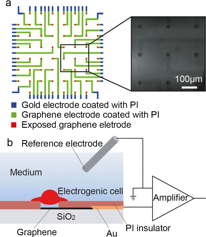
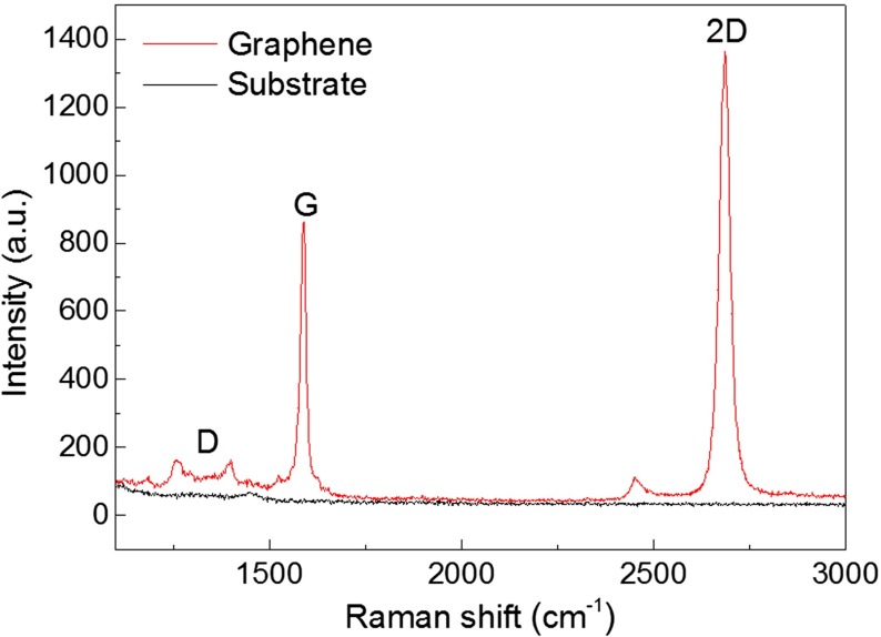
We start by briefly describing the fabrication techniques. Figure 1a shows the scheme for fabricating the graphene MEAs. The graphene electrodes were fabricated from commercially available chemical vapor deposit (CVD) graphene (Nanjing JCNANO Tech Co., Ltd., Nanjing, China). The graphene comes as poly(methyl methacrylate) (PMMA)/graphene/copper samples. The samples were first placed in an ammonium persulfate ((NH4)2 S2O8) solution (40 g/l, 37 °C) for 2–4 h to etch the copper. Iron trichloride (FeCl3) and iron (III) nitrate (Fe(NO3)3) solutions can also be used to etch the copper. (NH4)2 S2O8 was chosen because of its low contamination from dopants and low mobility degradation [15]. The resulting PMMA/graphene films were washed in deionized (DI) water several times and then transferred onto SiO2 (300 nm)/Si or quartz (ZS-1, 1 mm thick) substrates. The PMMA layer was removed by dipping the substrates in acetone (50 °C) for 4–6 h. The graphene substrates were then cleaned by rinsing in absolute alcohol and DI water and dried with a flow of nitrogen. Au/Ti electrodes were deposited and patterned so that the graphene MEAs were able to be connected to the amplifier. Then, lithography was performed to pattern the graphene electrodes and the undesired graphene was etched with oxygen plasma. A 1-μm-thick light-sensitive polyimide (PI) film was then spin-coated on the patterned graphene electrodes. Openings, 20 μm in diameter, were formed by PI lithography to expose the graphene electrode sites. After curing the PI layer, a 10-mm-diameter glass ring was glued to the MEA with polydimethylsiloxane (PDMS) to secure the region for subsequent cell culturing. The graphene MEAs on quartz substrates were used in the impedance measurement and action potential detection because they have transparent electrode sites, which are convenient to monitor cell growth under an inverted microscope. The quartz substrate itself has good transparency [16]. The transmittance of the 1-mm-thick quartz substrate is ∼90% in the wavelength range of 210-1,500 nm. Because of the high transmittance (>90%) of graphene [10], the graphene electrodes on quartz substrates also show good transparency [13]. The graphene MEAs on SiO2 (300 nm)/Si substrates were used for graphene observation and characterization because 300-nm-thick SiO2 can give an obvious color contrast to graphene [17], as shown in the inset of Fig. 1a. Figure 2 shows the Raman spectra of a graphene film on a SiO2 (300 nm)/Si substrate. A low density of the disorder-induced D band is observed around 1,350 cm−1, which largely comes from graphene edges or sub-domain boundaries. The intensity ratio of the G (∼1,589 cm−1) and 2D (∼2,686 cm−1) peaks (I (2D)/I (G)) is 1.59. Besides, the 2D peak also presents a sharp linewidth (33 cm−1) and a single Lorentzian profile, which are the hallmarks of monolayer graphene. In multilayer cases, the 2D peak has a wider linewidth and variable peak shapes [18–20].
Fig. 1.
a Structure of the graphene MEAs. The inset is an optical image of a graphene MEA on a SiO2 (300 nm)/Si substrate, where the scale bar represents 100 μm. b Diagram of one of the graphene microelectrodes used to record the action potential
Fig. 2.
Raman spectra of graphene sheets on SiO2 (300 nm)/Si and SiO2 (300 nm)/Si substrates
Electrochemical impedance measurement
Electrochemical impedance spectroscopy (EIS) was used to study the interfaces of graphene–electrolyte and gold (Au)–electrolytes. To obtain stable and repeatable results, electrodes (quartz substrates) with a large surface area (Au electrode, 0.12 cm2; graphene electrode, 0.07 cm2) were fabricated. All electrochemical impedances were measured with a potentiostat/galvanostat (IM6ex, ZAHNER-Elektrik GmbH & Co. KG, Kronach, Germany) and an incidental frequency response analyzer was used to analyze the electrochemical impedance. A three-electrode system was selected. The reference electrode was an Ag/AgCl electrode, the counter electrode was a platinum (Pt) wire and the graphene or Au electrode was used as the working electrode. The measurements were conducted in 50 mM phosphate buffer (PB) containing 50 mM potassium chloride (KCl). Before EIS measurement, the working electrode was electrochemically cleaned by cycling the potential over the range -0.6 to 0.6 V vs. Ag/AgCl (scan rate, 100 mV · s−1), until a stable voltammogram was obtained, and a reproducible a.c. spectrum could be achieved. The fitting level of the model was evaluated by the function χ2 defined as the sum of the squares of residuals. In the χ2 calculation, modulus weighting was chosen.
Furthermore, to compare the graphene MEAs with the Au MEAs in similar conditions, an Au MEA with the same electrode site area and the same insulation layer was also fabricated. A two-electrode system was used to assess the impedances of both MEAs. The Ag/AgCl electrode acted as the reference electrode and the graphene or Au electrode was used as the working electrode. These measurements were conducted in 10 mM phosphate buffered saline (PBS).
Action potential detection
To further study the applicability of graphene MEAs in recording action potentials, electrophysiological experiments were carried out. Before culturing, empty graphene MEAs with culture medium, which did not contain cells, were recorded from to confirm that they had a stable noise level. To detect the action potential, the devices were first sterilized in 70% ethanol and then they were washed with sterilized DI water. When dry, the graphene MEAs were coated with poly-d-lysine (0.1 mg/ml, Invitrogen Inc., Carlsbad, CA, USA) and stored overnight. Cortical cells were dissociated from Wistar rats (embryonic day 18) and plated to the graphene MEAs with a density of 400 cells/mm2. The cells were cultured in a Neurobasal medium (Invitrogen, Inc.) with 2% B27, 0.5 mM l-glutamate and 0.1% gentamicin. After 4 h, the whole medium was replaced to remove any unattached neurons. The devices were incubated at 37 °C in a 5% CO2 atmosphere. Half of the medium was changed every 3 days. After 14 days in vitro (DIV), the graphene MEA that contained neurons was connected to a MEA1060 amplifier (gain = 1,200, 10 Hz–3 kHz, Multi Channel Systems, Reutlingen, Germany). The amplified signals were fed into a data acquisition card (sampling rate 30 kHz, National Instruments, Austin, TX, USA). The data were then stored using LabVIEW. Figure 1b shows a diagram of one of the channels used to detect the action potential.
Results
Electrochemical impedance
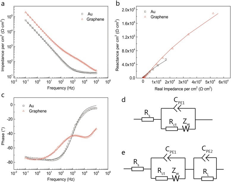
The impedance and phase curves of graphene and gold electrodes with a large area (Au electrode, 0.12 cm2; graphene electrode, 0.07 cm2) are shown in Fig. 3a and c, within the range 0.1 Hz–100 kHz. Corresponding Nyquist plots are shown in Fig. 3b. The values are normalized to per cm2. The Au electrode shows relatively low impedance, compared to the graphene electrode. The EIS of the Au electrode can be simulated with the Randles circuit, which is presented in Fig. 3d. The constant-phase element (CPE) CPE1, with a value of 25.84 μS · s0.86 · cm−2 , is consistent with the double-layer capacitance value level of dozens of μF·cm−2 [21–23]. For the graphene electrode, the interface is more complicated and cannot be well modeled by the structure in Fig. 3d. The EIS of the graphene electrode is variable, depending on the graphene states, like the manufacturing process of the graphene or whether the graphene is doped [11, 24]. The EIS of the graphene electrode in Fig. 3a and c can be well fitted by the model shown in Fig. 3f. Another constant-phase element CPE2 and a leakage resistance RL are added. CPE1 and CPE2 in Fig. 3f are about 8.21 μS · s0.67 · cm−2 and 7.94 μS · s0.91 · cm−2, respectively. Recent research has confirmed the existence of quantum capacitance in graphene [25, 26] and the graphene–electrolyte interface can be viewed as a series combination of the double layer capacitance and the quantum capacitance [23]. The quantum capacitance is evaluated to be several μF·cm−2 under a small gate voltage [23, 26]. The good fitting level of this model and the orders of magnitude of CPE1 and CPE2 can both confirm the existence of quantum capacitance, but whether CPE1 and CPE2 represent the double-layer and quantum capacitance respectively still needs further research, for example by studying the behavior of CPE1 and CPE2 on solutions with different concentrations and pHs. The fitting results are shown in Table 1. The corresponding χ2 of gold and graphene electrodes are 3.255 × 10⁻³ and 3.268 × 10⁻⁴ respectively.
Fig. 3.
Impedance (a) and phase (c) plots for graphene (0.12 cm2) and gold (0.07 cm2) electrodes. Corresponding Nyquist plots are shown in b. Measurement results are shown with symbols and fitting results are shown with solid lines. d, e Schematics for an equivalent circuit model used to fit the corresponding EIS results of gold and graphene electrodes. The values are normalized to per cm2
Table 1.
Fitting results for EIS measurements
| Au | Graphene | |
|---|---|---|
| Rs (Ω · cm2) | 17.98 | 12 |
| CPE1 (S · sn · cm−2) | 2.584 × 10⁻⁵ | 8.211 × 10⁻⁶ |
| n1 | 0.8615 | 0.6733 |
| Rct (Ω · cm2) | 5.421 × 10⁵ | 234.3 |
| Zw (S · s0.5 · cm−2) | 1.893 × 10⁴ | 1.161 × 10⁻⁴ |
| CPE2 (S · sn · cm−2) | 7.935 × 10⁻⁶ | |
| n2 | 0.9053 | |
| RL (Ω · cm2) | 1.641 × 10⁶ |
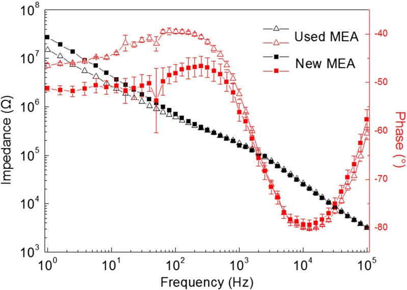
When it comes to graphene MEA with 20 μm in diameter, for five randomly selected graphene microelectrodes, the impedance is 170 ± 11.1 KΩ (mean = ± standard deviation (SD), frequency = 1 kHz). A similar electrode impedance was observed for the Au MEA with 20 μm in diameter, which is 186 ± 3.4 KΩ (mean = ± SD, frequency = 1 kHz). The electrochemical impedances of graphene electrodes with small and large areas show differences (Figs. 3 and 5). The model in Fig. 3e can also be used to fit the EIS of graphene MEA in Fig. 5.
Fig. 5.
Bode diagrams of graphene microelectrodes before (square) and after (triangle) cell culturing. Five electrodes were randomly selected
Action potential recording
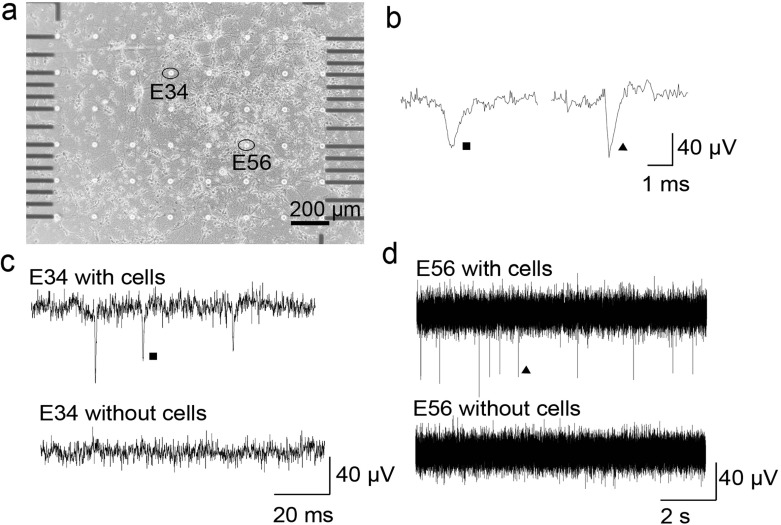
An empty graphene MEA with culture medium, which did not contain cells, presented a stable noise level (Fig. 4c, d). This indicated that the detection system itself did not introduce any confusing signals. Cortical cells were dissociated from Wistar rats (embryonic day 18) and plated onto the graphene MEAs with a density of 400 cells/mm2. After 14 DIV, spikes were detected by setting the threshold to five times the standard deviation of a 500-ms noise signal. The SNR was acquired by dividing the signal amplitude by the standard deviation of noise. Electrical activities were recorded from the neurons cultured on the graphene MEAs after 14 DIV (Fig. 4a). The spontaneous activities from electrodes 34 and 56 are shown in Fig. 4c, d. The spikes from these electrodes are enlarged in Fig. 4b. For the graphene MEAs, there were 60 active channels (channels presenting firing rates more than 0.01 Hz). The average firing rate was 1 Hz per electrode. The SNR of the detected signal was 10.31 ± 1.2 (mean = ± SD). This SNR is comparable to those of MEAs made with other materials [27].
Fig. 4.
a Neurons cultured on a graphene MEA (quartz substrate) after 14 DIV. The cells were dissociated from Wistar rats (embryonic day 18). c, d Spontaneous activities recorded from electrodes 34 and 56 with a SNR of 10.31 ± 1.2 and noise recorded from electrodes 34 and 56 without cells in the medium. b Shapes of the spontaneous spikes in c and d
Long-term stability
By continuously culturing neurons on the graphene MEAs, we were able to evaluate the durability of the graphene MEAs. The performance of a fresh graphene MEA was assessed and neurons were then cultured on it. After the MEA was cultured for 40 days, the cortical cells on the graphene MEA were removed by mechanical washing and trypsin digestion. After rinsing the MEA with deionized water, its electrode impedance was assessed again. For comparison, the two impedance curves before and after neuron culturing are presented in Fig. 5. The impedance of the used graphene electrode was 176 ± 2.5 KΩ at 1 kHz. This value was slightly higher than that of the fresh graphene electrode 170 ± 11.1 KΩ at 1 kHz. The small variation in the impedance verified the long-term stability of the MEAs.
Conclusions
In conclusion, we demonstrated a simple, yet inexpensive technique to fabricate graphene MEAs. The device takes advantage of graphene’s properties as it is able to provide high conductance, transparency, and excellent biocompatibility simultaneously. It successfully records the neural activities of primary cultured rat cortical neurons. Additionally, the fabricated graphene MEAs demonstrated excellent long-term stability in aqueous solutions. These results outline graphene’s great potential for use in detecting action potentials.
Acknowledgments
This work was supported by grants from the National Basic Research Program of China (973 Program) (Nos. 2011CB707505 and 2012CB933303), the National Science Foundation of China (Nos. 21275153 and 61271161), the Scientific Equipment Research Project of the Chinese Academy of Sciences (No. YZ201337), the CAS-Helmholtz joint research team (No. GJHZ1306) and the Science and Technology Project of Jiangsu Province, China (No. BE2012049).
References
- 1.Jimbo Y, Kawana A. Electrical-stimulation and recording from cultured neurons using a planar electrode array. Bioelectrochem. Bioenerg. 1992;29(2):193–204. doi: 10.1016/0302-4598(92)80067-Q. [DOI] [Google Scholar]
- 2.Egert U, Schlosshauer B, Fennrich S, Nisch W, Fejtl M, Knott T, Muller T, Hammerle H. A novel organotypic long-term culture of the rat hippocampus on substrate-integrated multielectrode arrays. Brain Res. Protoc. 1998;2(4):229–242. doi: 10.1016/S1385-299X(98)00013-0. [DOI] [PubMed] [Google Scholar]
- 3.Fofonoff TA, Martel SM, Hatsopoulos NG, Donoghue JP, Hunter IW. Microelectrode array fabrication by electrical discharge machining and chemical etching. IEEE Trans. Biomed. Eng. 2004;51(6):890–895. doi: 10.1109/TBME.2004.826679. [DOI] [PubMed] [Google Scholar]
- 4.Gross GW, Rhoades BK, Reust DL, Schwalm FU. Stimulation of monolayer networks in culture through thin-film indium-tin oxide recording electrodes. J. Neurosci. Meth. 1993;50(2):131–143. doi: 10.1016/0165-0270(93)90001-8. [DOI] [PubMed] [Google Scholar]
- 5.Geim AK, Novoselov KS. The rise of graphene. Nat. Mater. 2007;6(3):183–191. doi: 10.1038/nmat1849. [DOI] [PubMed] [Google Scholar]
- 6.Hess LH, Jansen M, Maybeck V, Hauf MV, Seifert M, Stutzmann M, Sharp ID, Offenhausser A, Garrido JA. Graphene transistor arrays for recording action potentials from electrogenic cells. Adv. Mater. 2011;23(43):5045–5049. doi: 10.1002/adma.201102990. [DOI] [PubMed] [Google Scholar]
- 7.Cohen-Karni T, Qing Q, Li Q, Fang Y, Lieber CM. Graphene and nanowire transistors for cellular interfaces and electrical recording. Nano Lett. 2010;10(3):1098–1102. doi: 10.1021/nl1002608. [DOI] [PMC free article] [PubMed] [Google Scholar]
- 8.Chen, C.H., Lin, C.T., Chen, J.J., Hsu, W.L., Chang, Y.C., Yeh, S.R., Li, L.J., Yao, D.J.: A graphene-based microelectrode for recording neural signals. In: 16th Int. Conf. on Solid-State Sensors, Actuators and Microsystems, Beijing, China, 5-9 Jun. 2011, pp. 1883–1886
- 9.Bendali A, Hess LH, Seifert M, Forster V, Stephan AF, Garrido JA, Picaud S. Purified neurons can survive on peptide-free graphene layers. Adv. Healthcare Mater. 2013;2(7):929–933. doi: 10.1002/adhm.201200347. [DOI] [PubMed] [Google Scholar]
- 10.Park D-W, Schendel AA, Mikael S, Brodnick SK, Richner TJ, Ness JP, Hayat MR, Atry F, Frye ST, Pashaie R, Thongpang S, Ma Z, Williams JC. Graphene-based carbon-layered electrode array technology for neural imaging and optogenetic applications. Nat. Commun. 2014;5:5258. doi: 10.1038/ncomms6258. [DOI] [PMC free article] [PubMed] [Google Scholar]
- 11.Kuzum D, Takano H, Shim E, Reed JC, Juul H, Richardson AG, de Vries J, Bink H, Dichter MA, Lucas TH, Coulter DA, Cubukcu E, Litt B. Transparent and flexible low noise graphene electrodes for simultaneous electrophysiology and neuroimaging. Nat. Commun. 2014;5:5259. doi: 10.1038/ncomms6259. [DOI] [PMC free article] [PubMed] [Google Scholar]
- 12.Kim KS, Zhao Y, Jang H, Lee SY, Kim JM, Kim KS, Ahn J-H, Kim P, Choi J-Y, Hong BH. Large-scale pattern growth of graphene films for stretchable transparent electrodes. Nature. 2009;457(7230):706–710. doi: 10.1038/nature07719. [DOI] [PubMed] [Google Scholar]
- 13.Bae S, Kim H, Lee Y, Xu X, Park J-S, Zheng Y, Balakrishnan J, Lei T, Ri Kim H, Song YI, Kim Y-J, Kim KS, Ozyilmaz B, Ahn J-H, Hong BH, Iijima S. Roll-to-roll production of 30-inch graphene films for transparent electrodes. Nat. Nanotechnol. 2010;5(8):574–578. doi: 10.1038/nnano.2010.132. [DOI] [PubMed] [Google Scholar]
- 14.Mailly-Giacchetti B, Hsu A, Wang H, Vinciguerra V, Pappalardo F, Occhipinti L, Guidetti E, Coffa S, Kong J, Palacios T. pH sensing properties of graphene solution-gated field-effect transistors. J. Appl. Phys. 2013;114(8):084505. doi: 10.1063/1.4819219. [DOI] [Google Scholar]
- 15.Wang YY, Burke PJ. A large-area and contamination-free graphene transistor for liquid-gated sensing applications. Appl. Phys. Lett. 2013;103(5):052103. doi: 10.1063/1.4816764. [DOI] [Google Scholar]
- 16.Zhuo H, Peng FC, Lin LM, Qu Y, Lai FC. Optical properties of porous anodic aluminum oxide thin films on quartz substrates. Thin Solid Films. 2011;519(7):2308–2312. doi: 10.1016/j.tsf.2010.11.024. [DOI] [Google Scholar]
- 17.Blake P, Hill EW, Castro Neto AH, Novoselov KS, Jiang D, Yang R, Booth TJ, Geim AK. Making graphene visible. Appl. Phys. Lett. 2007;91(6):063124. doi: 10.1063/1.2768624. [DOI] [Google Scholar]
- 18.Reina A, Jia XT, Ho J, Nezich D, Son HB, Bulovic V, Dresselhaus MS, Kong J. Large area, few-layer graphene films on arbitrary substrates by chemical vapor deposition. Nano Lett. 2009;9(1):30–35. doi: 10.1021/nl801827v. [DOI] [PubMed] [Google Scholar]
- 19.Ferrari AC, Meyer JC, Scardaci V, Casiraghi C, Lazzeri M, Mauri F, Piscanec S, Jiang D, Novoselov KS, Roth S, Geim AK. Raman spectrum of graphene and graphene layers. Phys. Rev. Lett. 2006;97(18):187401. doi: 10.1103/PhysRevLett.97.187401. [DOI] [PubMed] [Google Scholar]
- 20.Malard LM, Pimenta MA, Dresselhaus G, Dresselhaus MS. Raman spectroscopy in graphene. Phys. Rep. 2009;473(5–6):51–87. doi: 10.1016/j.physrep.2009.02.003. [DOI] [Google Scholar]
- 21.Piela, B., Wrona, P.K.: Capacitance of the gold electrode in 0.5 M H2SO4 solution: a.c. impedance studies. J. Electroanal. Chem. 388(1–2), 69-79 (1995). doi:10.1016/0022-0728(94)03848-W
- 22.Wang HN, Pilon L. Accurate simulations of electric double layer capacitance of ultramicroelectrodes. J. Phys. Chem. C. 2011;115(33):16711–16719. doi: 10.1021/jp204498e. [DOI] [Google Scholar]
- 23.Xia JL, Chen F, Li JH, Tao NJ. Measurement of the quantum capacitance of graphene. Nat. Nanotechnol. 2009;4(8):505–509. doi: 10.1038/nnano.2009.177. [DOI] [PubMed] [Google Scholar]
- 24.Casero E, Parra-Alfambra AM, Petit-Domínguez MD, Pariente F, Lorenzo E, Alonso C. Differentiation between graphene oxide and reduced graphene by electrochemical impedance spectroscopy (EIS) Electrochem. Commun. 2012;20:63–66. doi: 10.1016/j.elecom.2012.04.002. [DOI] [Google Scholar]
- 25.Chen, Z., Appenzeller, J.: Mobility extraction and quantum capacitance impact in high performance graphene field-effect transistor devices. In: Electron Devices Meeting, San Francisco, CA, 15-17 Dec. 2008, pp. 1-4
- 26.Fang T, Konar A, Xing H, Jena D. Carrier statistics and quantum capacitance of graphene sheets and ribbons. Appl. Phys. Lett. 2007;91(9):092109. doi: 10.1063/1.2776887. [DOI] [Google Scholar]
- 27.Cheng J, Zhu G, Wu L, Du X, Zhang H, Wolfrum B, Jin Q, Zhao J, Offenhausser A, Xu Y. Photopatterning of self-assembled poly (ethylene) glycol monolayer for neuronal network fabrication. J. Neurosci. Meth. 2013;213(2):196–203. doi: 10.1016/j.jneumeth.2012.12.020. [DOI] [PubMed] [Google Scholar]


