Abstract
Two-dimensional materials such as graphene and transition metal dichalcogenides have attracted great attention because of their rich physics and potential applications in next-generation nanoelectronic devices. The family of two-dimensional materials was recently joined by atomically thin black phosphorus which possesses high theoretical mobility and tunable bandgap structure. However, degradation of properties under atmospheric conditions and high-density charge traps in black phosphorus have largely limited its actual mobility thus hindering its future applications. Here, we report the fabrication of stable sandwiched heterostructures by encapsulating atomically thin black phosphorus between hexagonal boron nitride layers to realize ultra-clean interfaces that allow a high field-effect mobility of ∼1,350 cm2V−1 s−1 at room temperature and on–off ratios exceeding 105. At low temperatures, the mobility even reaches ∼2,700 cm2V−1 s−1 and quantum oscillations in black phosphorus two-dimensional hole gas are observed at low magnetic fields. Importantly, the sandwiched heterostructures ensure that the quality of black phosphorus remains high under ambient conditions.
 Black phosphorus is an atomically thin material that exhibits excellent properties for electronics applications, but these degrade in atmospheric conditions. Here, the authors demonstrate the fabrication of stable, ultra-clean and high-mobility black phosphorus sandwiched between the layers of boron nitride.
Two-dimensional (2D) materials with both high mobility and high on–off ratios are in demand for next-generation nanodevices. Graphene1,2, being the most widely studied material, has shown rich physics and high mobility, but the absence of a bandgap1,2 limits its applications. Analogous to 2D transition metal dichalcogenide structures3,4,5,6,7,8,9,10,11, atomically thin black phosphorus (BP)12,13,14,15 has recently evoked interest due to its high theoretical mobility16, tunable direct bandgap17,18,19,20 and ambipolarity12,13,14,15—unique properties that make it suitable for application in electronic and optoelectronic devices21,22,23. Recently, field-effect transistors (FETs)12,13,14,15,24,25,26, electrically tunable PN junctions22, radio-frequency transistors27 and heterojunctions28,29 based on few-layer BP have also been demonstrated. However, the room temperature mobility of few-layer phosphorene reported so far is limited to 400 cm2V−1 s−1 due to the presence of high-density charge traps, defects and phonon scattering12,13,14,15. The quality degradation of BP under atmospheric conditions is mainly due to its reaction with O2-saturated H2O30,31.
Here we demonstrate a high field-effect mobility of ∼1,350 cm2V−1 s−1 at room temperature and high on–off ratios exceeding 105 in few-layer phosphorene encapsulated by atomically thin hexagonal boron nitride (BN), which forms a stable BN–BP–BN heterostructure. A room temperature mobility of ∼1,000 cm2V−1 s−1 is rare in 2D semiconductor electron gas systems prepared by mechanical exfoliation techniques. In addition, the BN layers further avoids quality degradation of BP when exposed to atmosphere. At cryogenic temperatures, the mobility even reaches ∼2,700 cm2V−1 s−1 and Shubnikov-de Haas (SdH) oscillations are observed in BP at low magnetic fields (∼6 T). Our fabrication and treatment techniques for BN–BP–BN heterostructures open up a way to achieve high-performance 2D semiconductors with greatly improved room temperature mobility, on–off ratios and stability under ambient conditions for practical applications in high-speed electronic and optoelectronic devices.
Results
Fabrication of the sandwiched BP heterostructure devices
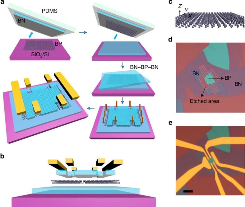
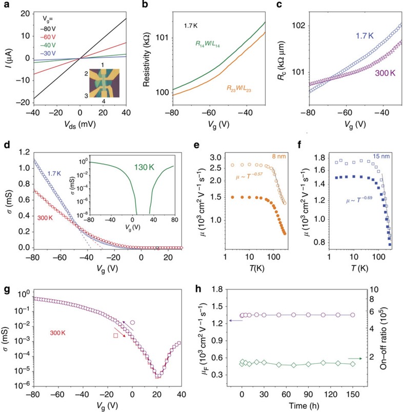
To achieve both high mobility and stability of BP FETs under atmospheric conditions, the BN–BP–BN configuration and high-temperature annealing are the two key factors. The ultra-clean BN–BP interfaces are ensured by adopting the polymer-free van der Waals transfer technique32 as shown in Fig. 1a. The few-layer BP mechanically exfoliated on a 300-nm SiO2/Si substrate was first picked up by a thin BN flake (6–20 nm thick). Then the BN–BP sample was transferred to a BN flake supported on a SiO2/Si substrate to form the BN–BP–BN heterostructure. The atomically thin BP was completely encapsulated by two BN layers, thus allowing us to anneal the sample at temperatures up to 500 °C in an argon atmosphere to further improve the sample quality. Without the BN protective layers, few-layer BP breaks down easily at 350 °C (see Supplementary Note 1 and Supplementary Fig. 1). In addition, the annealing process can significantly reduce the charge trap density in BP as no hysteresis effect is observed at room temperature (Fig. 2g and Supplementary Fig. 2).
Figure 1. BN–BP–BN heterostructure device.
(a) Schematic of the BN–BP–BN heterostructure device fabrication process. (b,e) Schematic (b) and optical image (e) of a BN–BP–BN Hall-bar device. Scale bar, 10 μm. (c) Atomic structure of monolayer BP. (d) The BN–BP–BN heterostructure after O2-plasma etching. The etched area is enclosed within the white line. The purple-dashed line denotes the lower BN layer.
Figure 2. Mobility and stability of the BN–BP–BN heterostructure devices.
(a) The I–Vds curves obtained at different gate voltages at 1.7 K. The inset is the optical image of Sample A with the following geometrical parameters: L14=16 μm, L23=10 μm and W=3 μm. (b) The resistivity determined from four-terminal (green line) and two-terminal configurations (orange line) at 1.7 K. (c) Variation of the contact resistivity. (d) The conductivity of Sample A measured at with a room temperature and 1.7 K. The inset shows the ambipolarity of the BP conductance. (e,f) Temperature dependence of the field-effect μF (open dots) and Hall mobilityμh (solid dots) at Vg=−70 V) of Sample A and Sample B (15 nm thick). The dashed lines serve as guidelines for the μ∼T−γ relation. (g) The room temperature conductivity showing no hysteresis in Sample A. (h) The mobility and on–off ratio of Sample A as a functions of ambient exposure time. No quality degradation is observed even after exposure for an entire week.
Instead of using one-dimensional edge-contact32 that has been proven effective for graphene-encapsulated structures (but less so for 2D semiconductors), we developed the area contact technique for contacting the encapsulated 2D semiconductors. Beginning with the BN–BP–BN heterostructure, a hard mask is defined by the standard electron-beam lithography technique using ZEP-520 resist (detailed process is shown in Supplementary Note 2 and Supplementary Fig. 3). Since the O2-plasma etching rates for BN and BP are different, the BN layers can be quickly etched while the BP layer still survive as shown in Fig. 1d. Lastly, Cr/Au (2 nm/60 nm) electrodes are deposited using electron-beam lithography technique. Figure 1b,e show the schematic and optical image of a BN–BP–BN Hall-bar device respectively. Note that no further annealing process is needed after deposition of the electrodes.
Mobility and stability of the sandwiched BP devices
Figure 2a shows the I–Vds characteristic of an 8-nm-thick BN–BP–BN sample (Sample A). The linear I–Vds characteristic indicates that Ohmic contacts have been achieved on the hole side. By comparing the resistivity directly measured using the two-terminal configuration (R14W/L14) with that extracted using the four-terminal configuration (R23W/L23), the contact resistivity is obtained (Fig. 2b). As shown in Fig. 2c, the contact resistivity measured at high gate voltages is about several  when the sample temperature is sufficiently low and thermal activation effects are suppressed. The contact resistivity decreases with decreasing temperature when the gate voltage Vg<−68 V, further verifying the good contacts between BP and Cr/Au electrodes on the hole side.
The BN–BP–BN heterostructure exhibits high quality as is first confirmed by examining the four-terminal field-effect (FET) mobility 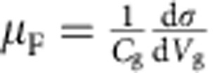 at different temperatures, where σ is the conductivity and Cg is the gate capacitance. Figure 2d shows the conductivity as a function of gate voltage for Sample A. Similar to the results reported previously, both hole and electron conductance can be achieved (see the inset in Fig. 2d). Here we mainly focus on the hole conductance due to its higher mobility. The gate capacitance Cg is calculated to be 1.1 F cm−2 based on the thickness of SiO2 (300 nm) and the lower BN layer (∼15 nm as determined by atomic force microscopy). With this information, we extracted the hole μF from the linear part of conductance at different temperatures (Fig. 2e,f). As shown in Fig. 2d, we achieved a high FET mobility μF∼1,350 cm2V−1 s−1 and Hall mobility μH∼790 cm2V−1 s−1 for Sample A at room temperature. Another four BN–BP–BN heterostructures also exhibit high mobility (∼800 cm2V−1 s−1) at room temperature (summarized in Supplementary Table 1). One possible reason for the high mobility in our BP samples is because their transport directions are nearly along the fast X-direction (see Fig. 1c) as confirmed by angle-dependent polarized Raman spectroscopy (see Supplementary Note 3 and Supplementary Fig. 4). The mobility along the X-direction can be two times larger than that along the Y-direction13,15. The transport-direction of Sample A is parallel to the X-direction. Although the mobility we achieved is still smaller than the values measured from bulk BP (∼2,000 cm2V−1 s−1)33, it is much larger than that observed in atomically thin MoS2 (refs 3, 4, 10) and few-layer BP supported on SiO2 (refs 12, 13, 14, 15). Theoretical calculations for few-layer BP16 indicate that a hole mobility over 4,000 cm2V−1 s−1 is achievable along the X-direction at room temperature. Hence, the quality improvement is still the critical limiting factor for the mobility of few-layer BP.
The high quality of the BN–BP–BN heterostructure is further confirmed by the observation of a high on–off ratio exceeding 105 and insignificant hysteresis at room temperature (Fig. 2g), while previous work14 on BP supported on SiO2 showed a pronounced hysteresis (ΔVg∼80 V) depending on the sweep direction at room temperature, indicating the presence of a high density of charge traps. The small charge trap density in our BN–BP–BN heterostructure is due not only to the ultra-clean BN–BP interfaces but also to the high-temperature annealing (300–500 °C) of the encapsulated BP. As shown in Supplementary Fig. 2, in a BN–BP–BN heterostructure device without annealing, we observed a hysteresis ΔVg∼10 V, which is much smaller than that observed in BP supported on SiO2. Supplementary Note 4 and Supplementary Fig. 5 demonstrate the mobility changes of Sample D before and after annealing. The mobility of this sample measured at cryogenic and room temperatures indeed increases significantly. These results verified that high-temperature annealing can effectively suppress charge trap states and further improve the mobility and on–off ratio of BP devices.
The stability of the electrical performance of the BN–BP–BN heterostructure is examined under ambient conditions (with humidity around 60%). As shown in Fig. 2h, the mobility and on–off ratios show no degradation even after exposure to ambient conditions for a whole week. Obviously, the BN–BP–BN heterostructure completely hides the BP layer from ambient conditions and prevents it from reacting with O2-saturated H2O. With its high room temperature mobility, on–off ratios and stability, the BN–BP–BN heterostructure is a promising candidate for practical applications in electronic and optoelectronic devices.
At 1.7 K, the mobility of Sample A reaches ∼2,700 cm2V−1 s−1 (Fig. 2d) and the Hall mobility  is ∼1,500 cm2V−1 s−1 at large gate voltages, where nH is the carrier density from Hall measurement, which is equal to the value extracted from the gate capacitance model n=Cg(Vg–Vth)/e (see Supplementary Note 5 and Supplementary Fig. 6). The on–off ratios exceed 108 at 1.7 K. The temperature dependence of the FET and Hall mobility of the BN–BP–BN heterostructures (Fig. 2e,f) shows a similar trend as reported previously for few-layer phosphorene12 and monolayer MoS2 (ref. 4). The mobility saturates at low temperatures (T<80 K), but follows the expression μ∼T−γ at higher temperatures (T>80 K) due to phonon scattering. The extracted value γ is ∼0.57 for Sample A and ∼0.69 for Sample B (15 nm thick). These γ values are consistent with the ones observed in monolayer MoS2 covered with high-κ dielectric4 and few-layer phosphorene12, but are smaller than those found in bulk BP34 and other 2D materials35. Similar to the results reported previously12,13,15, the values of the Hall mobility measured from our samples are always smaller than that of their FET mobility (Supplementary Table 1). We believe that although charge traps are effectively suppressed in our BN–BP–BN heterostructures through annealing, other types of defects/impurities, such as vacancies and strain induced during the transfer process may still exist. These defects limit the mobility of few-layer BP particularly at low temperatures.
Quantum oscillations in the sandwiched BP devices
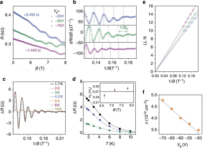
The quantum oscillations observed at magnetic fields B>6 T also attest to the high quality of BN–BP–BN heterostructures. Resistance at different gate voltages shows a negative magneto-resistance (Fig. 3a), indicating a weak localization effect36 previously observed in 2D electron gas systems containing disorder. In this kind of 2D electron gas systems, the time-reversal symmetry of the closed electron path is broken when a magnetic field is applied and the back scattering of electrons is suppressed resulting in a negative correction to the resistance. When B>6 T (corresponding to a mobility of ∼1/B near 1,670 cm2V−1 s−1), we start to see SdH oscillations at higher gate voltages where the Hall mobility becomes sufficiently high (Fig. 3a). The oscillation features are seen clearly in the form of dR/dB as shown in Fig. 3b (also see the data of Sample B in Supplementary Note 6 and Supplementary Figs 7 and 8).
Figure 3. SdH oscillations in the 8-nm-thick BN–BP–BN heterostructure.
(a) Resistance (R) plotted as a function of the magnetic field at gate voltages of −50 V (blue dots), −60 V (green dots) and −70 V (purple dots). (b) dR/dB plotted as a function of 1/B. The dashed lines indicate the oscillation period (increasing with gate voltages) of 1/BF. (c) ΔR plotted as a function of 1/B at Vg=−60 V for different temperatures. (d) Fitting of the experimental results (dots) using the Lifshitz–Kosevich formula (solid line). The inset shows the fitting results of the cyclotron mass. (e) Landau diagram at different gate voltages that shows a Berry phase β=0. (f) The carrier densities determined from LL fitting (orange dots) and gate capacitance (purple line).
The period of SdH oscillations37,38 in 2D electron gas is 1/BF and the longitudinal resistance is given by ΔR=R(B,T)cos[2π(BF/B+1/2+β)], where R(B,T) is the amplitude and β (0≤β≤1) is the Berry phase. β is known to be 0 in conventional 2D electron gas systems and 1/2 in graphene1,2. To examine the 2D nature of hole gas in few-layer BP, we plot dR/dB as a function of 1/B for different gate voltages. As shown in Fig. 3b, the oscillations at different gate voltages are periodic but exhibit different frequencies. A smaller period 1/BF is observed at higher gate voltages where the carrier density n is larger, which is consistent with the theoretical oscillation period37 expressed as 1/BF=2/Φ0n, where Φ0=4.14 × 10⁻¹⁵ Tm2 is the flux quantum. For example, at Vg=−50 V the oscillation period is ∼0.0138 T−1, corresponding to a carrier density of ∼3.5 × 1012 cm−2, which is in excellent agreement with the value obtained from the gate capacitance model n=Cg(Vg−Vth)/e (Fig. 3f). To further reveal the 2D nature of the charge carriers in few-layer BP, we carried out experiments to investigate the angular dependence of the SdH oscillations. The linear dependence between the magnetic field BF and 1/cos θ confirms that the charge carriers in few-layer BP are in 2D nature, where θ is the tilting angle between the applied magnetic fields and the normal direction of the substrate plane (see Supplementary Note 7 and Supplementary Fig. 9). The Landau level (LL) index N is plotted and the linear fit yields a Berry phase β=0 in our BP samples (Fig. 3e). A smaller LL index would be achieved if magnetic fields could be further increased.
The cyclotron effective mass mc of hole carriers in few-layer BP can be obtained by fitting the temperature dependence of resistivity ΔR (see Fig. 3c) using the Lifshitz–Kosevich formula AT∝T/sinh (2π2kBTmc/ℏeB), where kB is the Boltzmann constant. We fit ΔR at high magnetic fields to gain a better resolution as shown in Fig. 3d. The fitting results produce a cyclotron effective mass 0.27±0.02 me at Vg=−60 V. Owing to structural anisotropy, the carrier effective mass in few-layer BP is also highly anisotropic. Previous theoretical analyses16 show that the effective masses along the X- and Y- directions are mx∼0.14 me and my∼0.89 me respectively. The measured cyclotron effective mass in our BP samples is ∼0.27me, which is reasonable as compared with the theoretical value  for few-layer BP16.
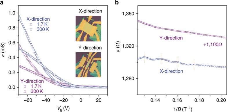
Finally, we designed a special sample (Sample C, 10 nm thick) to demonstrate the effects of transport anisotropy on the SdH oscillations in BP. First, this sample was cut along the X-direction (Fig. 4a). The Hall mobility was ∼1,481 cm2V−1 s−1 at 1.7 K (∼716 cm2V−1 s−1 at room temperature). The SdH oscillations are clearly visible in Fig. 4b when the magnetic field is higher than 6 T. Then, the sample was reshaped along the Y-direction (see the inset in Fig. 4a). The Hall mobility changed to ∼820 cm2V−1 s−1 at 1.7 K (∼365 cm2V−1 s−1 at room temperature). This experimental results are consistent with the conclusions in previous reports15,33. However, the magneto-resistivity in this reshaped sample (along the Y-direction) did not show any signature of SdH oscillations with magnetic fields up to 8 T. A much stronger magnetic field is needed to observe SdH oscillations in the sample.
Figure 4. SdH oscillations in the BN–BP–BN heterostructure samples along the X- and Y- directions.
(a) The conductivity of Sample C along the X- and Y- directions at 1.7 K and 300 K. The insets are optical images of Sample C before and after reshaping. (b) SdH oscillations measured at Vg=−60 V from the samples along the X- and Y- directions.
Discussion
In summary, we have demonstrated high-quality BN–BP–BN heterostructures achieved by encapsulating atomically thin BP between BN layers followed by annealing at high temperature. The BN–BP–BN heterostructure protects BP from property degradation and allows us to investigate the intrinsic properties of BP. The BN–BP–BN samples show excellent stability in the atmospheric environment with a high mobility ∼1,350 cm2V−1 s−1 and a large on–off ratio exceeding 105. Quantum oscillations and zero Berry phase are observed in BP hole gas at a magnetic field of 6 T at cryogenic temperatures. The ultra-clean interfaces realized by our fabrication process can effectively suppress charge trap states. They shed important light on how to improve the quality of atomically thin BP for practical applications in BP-based nanoelectronic devices.
Methods
Sample preparation and transport measurements
Bulk phosphorus and BN crystals (Polartherm grade PT110) were purchased from Smart-elements and Momentive, respectively. All atomically thin flakes were mechanically exfoliated by the scotch-tape microcleavage method. The thickness of BN and BP flakes was determined using an atomic force microscope (Veeco-Innova). The BN–BP–BN heterostructure was fabricated using the polymer-free van der Waals transfer technique32. The encapsulated BP was annealed in an argon atmosphere at 300–500 °C for 8 h before the upper BN layer was etched. No further annealing process was needed after deposition of the electrodes. Electrical measurements were performed using lock-in techniques in a cryogenic system (1.7–300 K and magnetic field up to 8 T).
Additional information
How to cite this article: Chen, X. et al. High quality sandwiched black phosphorus heterostructure and its quantum oscillations. Nat. Commun. 6:7315 doi: 10.1038/ncomms8315 (2015).
Supplementary Material
Supplementary Figures 1-9, Supplementary Tables 1, Supplementary Notes 1-7 and Supplementary References.
Acknowledgments
Financial support from the Research Grants Council of Hong Kong (Project Nos HKU9/CRF/13G, 604112, HKUST9/CRF/08 and N_HKUST613/12) and technical support of the Raith-HKUST Nanotechnology Laboratory for the electron-beam lithography facility at MCPF (Project No. SEG_HKUST08) are hereby acknowledged.
Footnotes
Author contributions N.W. and X.C. conceived the projects. X.C. and Y.W. conducted most experiments including sample fabrication, data collection and analyses. N.W. is the principle investigator and coordinator of this project. X.C. and N.W. provided the physical interpretation and wrote the manuscript. Other authors provided technical assistance in sample preparation, data collection/analyses and experimental set-up.
References
- Zhang Y. B., Tan Y. W., Stormer H. L. & Kim P. Experimental observation of the quantum Hall effect and Berry's phase in graphene. Nature 438, 201–204 (2005). [DOI] [PubMed] [Google Scholar]
- Novoselov K. S. et al. Electric field effect in atomically thin carbon films. Science 306, 666–669 (2004). [DOI] [PubMed] [Google Scholar]
- Radisavljevic B., Radenovic A., Brivio J., Giacometti V. & Kis A. Single-layer MoS2 transistors. Nat. Nanotechnol. 6, 147–150 (2011). [DOI] [PubMed] [Google Scholar]
- Radisavljevic B. & Kis A. Mobility engineering and a metal-insulator transition in monolayer MoS2. Nat. Mater. 12, 815–820 (2013). [DOI] [PubMed] [Google Scholar]
- Zhu W. J. et al. Electronic transport and device prospects of monolayer molybdenum disulphide grown by chemical vapour deposition. Nat. Commun. 5, 3087 (2014). [DOI] [PubMed] [Google Scholar]
- Novoselov K. S. et al. Two-dimensional atomic crystals. Proc. Natl Acad. Sci. USA 102, 10451–10453 (2005). [DOI] [PMC free article] [PubMed] [Google Scholar]
- Schmidt H. et al. Transport properties of monolayer MoS2 grown by chemical vapor deposition. Nano Lett. 14, 1909–1913 (2014). [DOI] [PubMed] [Google Scholar]
- Chen X. et al. Probing the electron states and metal-insulator transition mechanisms in molybdenum disulphide vertical heterostructures. Nat. Commun. 6, 6088 (2015). [DOI] [PubMed] [Google Scholar]
- Lopez-Sanchez O., Lembke D., Kayci M., Radenovic A. & Kis A. Ultrasensitive photodetectors based on monolayer MoS2. Nat. Nanotechnol. 8, 497–501 (2013). [DOI] [PubMed] [Google Scholar]
- Baugher B. W. H., Churchill H. O. H., Yang Y. F. & Jarillo-Herrero P. Intrinsic electronic transport properties of high-quality monolayer and bilayer MoS2. Nano Lett. 13, 4212–4216 (2013). [DOI] [PubMed] [Google Scholar]
- Wang Q. H., Kalantar-Zadeh K., Kis A., Coleman J. N. & Strano M. S. Electronics and optoelectronics of two-dimensional transition metal dichalcogenides. Nat. Nanotechnol. 7, 699–712 (2012). [DOI] [PubMed] [Google Scholar]
- Li L. K. et al. Black phosphorus field-effect transistors. Nat. Nanotechnol. 9, 372–377 (2014). [DOI] [PubMed] [Google Scholar]
- Liu H. et al. Phosphorene: an unexplored 2D semiconductor with a high hole mobility. ACS Nano 8, 4033–4041 (2014). [DOI] [PubMed] [Google Scholar]
- Koenig S. P., Doganov R. A., Schmidt H., Neto A. H. C. & Ozyilmaz B. Electric field effect in ultrathin black phosphorus. Appl. Phys. Lett. 104, 103106 (2014). [Google Scholar]
- Xia F. N., Wang H. & Jia Y. C. Rediscovering black phosphorus as an anisotropic layered material for optoelectronics and electronics. Nat. Commun. 5, 4458 (2014). [DOI] [PubMed] [Google Scholar]
- Qiao J. S., Kong X. H., Hu Z. X., Yang F. & Ji W. High-mobility transport anisotropy and linear dichroism in few-layer black phosphorus. Nat. Commun. 5, 4475 (2014). [DOI] [PMC free article] [PubMed] [Google Scholar]
- Zhu Z. & Tomanek D. Semiconducting layered blue phosphorus: a computational study. Phys. Rev. Lett. 112, 176802 (2014). [DOI] [PubMed] [Google Scholar]
- Rodin A. S., Carvalho A. & Castro Neto A. H. Strain-induced gap modification in black phosphorus. Phys. Rev. Lett. 112, 176801 (2014). [DOI] [PubMed] [Google Scholar]
- Das S. et al. Tunable transport gap in phosphorene. Nano Lett. 14, 5733–5739 (2014). [DOI] [PubMed] [Google Scholar]
- Guan J., Zhu Z. & Tománek D. Phase coexistence and metal-insulator transition in few-layer phosphorene: a computational study. Phys. Rev. Lett. 113, 046804 (2014). [DOI] [PubMed] [Google Scholar]
- Buscema M. et al. Fast and broadband photoresponse of few-layer black phosphorus field-effect transistors. Nano Lett. 14, 3347–3352 (2014). [DOI] [PubMed] [Google Scholar]
- Buscema M., Groenendijk D. J., Steele G. A., van der Zant H. S. J. & Castellanos-Gomez A. Photovoltaic effect in few-layer black phosphorus PN junctions defined by local electrostatic gating. Nat. Commun. 5, 4651 (2014). [DOI] [PubMed] [Google Scholar]
- Wang X. et al. Highly anisotropic and robust excitons in monolayer black phosphorus. Preprint at http://arxiv.org/abs/1411.1695 (2014). [DOI] [PubMed]
- Du Y., Liu H., Deng Y. X. & Ye P. D. Device perspective for black phosphorus field-effect transistors: contact resistance, ambipolar, behavior, and scaling. ACS Nano 8, 10035–10042 (2014). [DOI] [PubMed] [Google Scholar]
- Na J., Lee Y. T., Lim J. A., Hwang D. K. & Kim G. T. Few-layer black phosphorus field-effect transistors with reduced current fluctuation. ACS Nano 8, 11753–11762 (2014). [DOI] [PubMed] [Google Scholar]
- Das S., Demarteau M. & Roelofs A. Ambipolar phosphorene field effect transistor. ACS Nano 8, 11730–11738 (2014). [DOI] [PubMed] [Google Scholar]
- Wang H. et al. Black phosphorus radio-frequency transistors. Nano Lett. 14, 6424–6429 (2014). [DOI] [PubMed] [Google Scholar]
- Deng Y. X. et al. Black phosphorus-monolayer MoS2 van der Waals heterojunction p-n diode. ACS Nano 8, 8292–8299 (2014). [DOI] [PubMed] [Google Scholar]
- Yuan H. et al. Broadband linear-dichroic photodetector in a black phosphorus vertical p-n Junction. Preprint at http://arxiv.org/abs/1409.4729 (2014).
- Wood J. D. et al. Effective passivation of exfoliated black phosphorus transistors against ambient degradation. Nano Lett. 14, 6964 (2014). [DOI] [PubMed] [Google Scholar]
- Castellanos-Gomez A. et al. Isolation and characterization of few-layer black phosphorus. 2D Mater. 1, 025001 (2014). [Google Scholar]
- Wang L. et al. One-dimensional electrical contact to a two-dimensional material. Science 342, 614–617 (2013). [DOI] [PubMed] [Google Scholar]
- Morita A. Semiconducting black phosphorus. Appl. Phys. A 39, 227–242 (1986). [Google Scholar]
- Akahama Y., Endo S. & Narita S. Electrical-properties of black phosphorus single-crystals. J. Phys. Soc. Jpn 52, 2148–2155 (1983). [Google Scholar]
- Kaasbjerg K., Thygesen K. S. & Jacobsen K. W. Phonon-limited mobility in n-type single-layer MoS2 from first principles. Phys. Rev. B 85, 115317 (2012). [Google Scholar]
- Lee P. A. & Ramakrishnan T. V. Disordered electronic systems. Rev. Mod. Phys. 57, 287–337 (1985). [Google Scholar]
- Luk'yanchuk I. A. & Kopelevich Y. Phase analysis of quantum oscillations in graphite. Phys. Rev. Lett. 93, 166402 (2004). [DOI] [PubMed] [Google Scholar]
- Zhou X. Y. et al. Landau levels and magneto-transport property of monolayer phosphorene. Preprint at http://arxiv.org/abs/1411.4275 (2014). [DOI] [PMC free article] [PubMed]
Associated Data
This section collects any data citations, data availability statements, or supplementary materials included in this article.
Supplementary Materials
Supplementary Figures 1-9, Supplementary Tables 1, Supplementary Notes 1-7 and Supplementary References.


