

Abstract
In this work, we have studied thermoelectric properties of monolayer and fewlayer MoS2 in both armchair and zigzag orientations. Density functional theory (DFT) using non-equilibrium Green’s function (NEGF) method has been implemented to calculate the transmission spectra of mono- and fewlayer MoS2 in armchair and zigzag directions. Phonon transmission spectra are calculated based on parameterization of Stillinger-Weber potential. Thermoelectric figure of merit, ZT, is calculated using these electronic and phonon transmission spectra. In general, a thermoelectric generator is composed of thermocouples made of both n-type and p-type legs. Based on our calculations, monolayer MoS2 in armchair orientation is found to have the highest ZT value for both p-type and n-type legs compared to all other armchair and zigzag structures. We have proposed a thermoelectric generator based on monolayer MoS2 in armchair orientation. Moreover, we have studied the effect of various dopant species on thermoelectric current of our proposed generator. Further, we have compared output current of our proposed generator with those of Silicon thin films. Results indicate that thermoelectric current of MoS2 armchair monolayer is several orders of magnitude higher than that of Silicon thin films.
The advent of Graphene1,2,3, a two-dimensional (2D) sheet of carbon atoms in honeycomb lattice, has stimulated great interest and intensive research on the properties of 2D materials. More recently, a new family of 2D materials has been proposed, namely Transition Metal Dichalcogenides (TMDs). The presence of a bandgap in some members of TMD family, a crucial property for microelectronics applications, has attracted much attention in comparison with the gapless Graphene. Among all semiconducting TMDs, Molybdenum disulfide (MoS2) is the most representative, widely interesting and intensively studied one4,5,6, partially because it is relatively stable and readily available. MoS2 has been used as a dry lubricant in automobile industry due to its low friction properties. Recently, it has been studied for applications in field effect transistors7,8,9, photovoltaics10 and photocatalysis11.
In general, bulk TMDs has a layered structure. Each layer is formed by a plane of transition metal atoms sandwiched between two planes of chalcogen atoms in trigonal prismatic arrangements as illustrated in Fig. 1. Strong intralayer covalent bonding, in contrast to weak interlayer van der Waals forces12 make it possible to fabricate high-quality monolayer MoS2 by exfoliation technique12,13,14. A desirable bandgap12,13,14,15, comparable carrier mobility with those of Si thin film and Graphene nanoribbons14,16,17 together with excellent thermal stability14 and surface free from dangling bonds18,19, makes 2D MoS2 a very attractive candidate for device applications20,21.
Figure 1. Atomic structure of MoS2.

(a) Monolayer of MoS2 is made of a honeycomb sheet of Molybdenum atoms covalently sandwiched between two honeycomb sheets of Sulphur atoms. Bulk of MoS2 is formed by monolayers stacked and held on top of each other by van der Waals forces. Side view of mono-, bi-, tri- and quadlayer is illustrated in parts (b–e), respectively.
Compared to the research progress in its electronic and mechanical characteristics22,23,24, thermoelectric (TE) properties of MoS2 have not been widely studied. Thermoelectrics provide a way of converting thermal energy into electricity25. Thermoelectric generator is expected to play an important role in increasing demand for clean energy in future33. In general, a TE generator module is made of an array of thermocouples. As illustrated in Fig. 2, each thermocouple, the basic unit of a TE generator, is made of a p-type and an n-type semiconductor, named as legs, connected thermally in parallel and electrically in series. Temperature gradient across thermocouple is the driving force inducing electrical current.
Figure 2. Structure of proposed thermoelectric generator based on monolayer MoS2.

It is composed of a p-type and an n-type semiconductor, known as legs. Temperature gradient across thermocouples will induce an electrical current through thermocouple based on thermoelectric phenomenon.
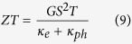
The research on thermoelectric materials has been one of the major topics since 1950 s when basic science of thermoelectrics was well founded26. Bi2Te3 and the similar alloys have played a main role in the application of thermoelectric devices. It is well-known that efficiency of thermoelectric conversion can be evaluated by a dimensionless figure of merit  , in which
  ,
,  , ke, kph and T are electrical conductance, Seebeck’s coefficient, electronic contribution to thermal conductance, phonon contribution to thermal conductance and absolute temperature, respectively26. In order to have a high ZT, it is desirable to have a high electrical conductance and large Seebeck’s coefficient and low thermal conductance. These parameters mainly depend on the intrinsic properties of materials and they are generally coupled with each other. Enhancement to one of them may degrade the other and the overall effect will not change. In three decades after 1950 s, only incremental progress was made due to the difficulty in fine-tuning of these parameters27.
Recently, new wave of research on thermoelectric field has been initiated because nanoscale structures may enhance thermoelectric efficiency. It was shown that quantum confinement of charge carriers in quantum-well super-lattices28, quantum-wires29 as well as bulk samples containing nanostructured constituents27 will enhance thermoelectric conversion. It is known that Density of States (DOS) of low-dimensional materials exhibits sharp changes around Fermi level27,28,29. As a result, Seebeck’s coefficient, which depends on logarithmic derivative of DOS, is significantly enhanced, and hence, the ZT increases. In addition to an increase in Seebeck’s coefficient, low dimensional materials are known to benefit from higher phonon scattering and consequently lower phonon thermal conductance27. Low phonon thermal conductivity (kph) has been already reported for TMDs:  ph of MoS2 thin films and disordered layered WSe2 are about 0.1 W/mK to 1 W/mK30 and 0.05 W/mK31, respectively. In addition, it has been reported that MoS2 has anisotropic thermal properties32, which provides another degree of freedom to optimize TE conversion performance. The advantage of nano-scale structures with respect to their bulk counterparts motivates us to study thermoelectric properties of 2D MoS2 in both armchair and zigzag orientations.
In this work, thermoelectric properties of mono-, bi-, tri- and quadlayer MoS2 in armchair and zigzag directions have been studied for electricity generation. ZT of bulk MoS2 has already been reported to be 0.1 at 700 K33. In a later study, effect of pressure on thermoelectric properties of MoS2 has been investigated34. ZT has been reported to increase up to 0.65 in a wide range of pressure and temperature. Thermoelectric performance of monolayer MoS2 has been studied and ZT is reported to reach 0.58 in room temperature35. In this study, ZT values up to 1.2 in armchair direction has been achieved which is higher than ZT values reported for omnidirectional MoS2 structures. Well-established thermoelectric materials include PbTe36,37 and Bi2Te338 based alloys, from which higher ZT values around 2.4 have been already achieved at 900 K. However, their substitution with abundant materials is favorable due to scarcity of Te element. This study aims to investigate the possibility of forming high performance thermoelectric generator based on highly available MoS2. In addition to abundance of MoS2, mono- and fewlayer structures have benefits of possibility of forming high density thermoelectric modules, due to their nano-scale size. In this study, it is found that as the number of layers increases from monolayer to quadlayer, both transmission spectrum and phonon thermal conductance increase. In addition, strong electronic and thermal transport anisotropy is found between zigzag and armchair orientations. Transmission coefficient and phonon thermal conductance of zigzag orientation is higher than those of armchair with the same number of layers. Their effect on ZT has been studied in this work. In addition, TE conversion of Si thin film TE generator with the same thickness as MoS2 armchair mono- and fewlayer TE generator has been studied by using Synopsys TCAD software. The comparison indicates that proposed MoS2 generator exhibits superior TE conversion efficiency.
Method
The computational model used in this paper is based on self-consistent density functional theory (DFT) using non-equilibrium Green’s function (NEGF) method39,40 implemented in QuantumWise ATK software package. Prior to the calculations of carrier transport, the structure has been relaxed to optimized force and stress of 0.05 eV/Å and 0.05 eV/ Å3, respectively. The relaxation calculations is implemented by using Generalized Gradient Approximation (GGA) exchange correlation with a Double Zeta Polarized (DZP) basis set and a mesh cut-off energy of 75 Ha.
Top view of structures studied in this paper is illustrated in Fig. 3. They can be divided into three regions: left, right and central. Left and right regions are called electrodes, treated with semi-infinite boundary conditions. Their properties can be described by solving for the bulk material. The voltage and temperature bias are applied on electrode regions. Central region includes a repetition of each electrode region in order to screen out perturbations introduced in the scattering regions. In order to have an insight on the effect of lattice orientation and thickness on the intrinsic TE properties of MoS2, no perturbation is introduced in the scattering region in calculating ZT.
Figure 3. Simulated structures in this paper.

Armchair-oriented and zigzag-oriented MoS2 are shown in part (a,b), respectively. Each device is comprised of three regions: left electrode, central region and right electrode. Central region, itself, contains an extension of electrode regions on both sides and scattering region in the middle. Electrode regions are treated semi-infinitely. Their properties are computed by solving for bulk material. Temperature gradient is biased on electrode regions. Extension of electrode regions in central region, are used to screen out any perturbation introduced in scattering region.
Central region shown in Fig. 3, should be large enough to accommodate both the voltage and temperature drop within itself. Due to computational constraints, we used 149, 299, 449 and 599 atoms supercell as central region in mono-, bi-, tri- and quadlayer structures, respectively. Using infinitesimal voltage and temperature drop, i.e. working in linear regime, makes our approximation valid. In addition, a vacuum spacing of 20 Å is added to each side of the structure super cell to suppress any interaction caused by periodic boundary condition at out-of-plane direction.
In order to calculate linear transport properties of the system, Landauer-Buttiker41 formula is used, in which transport coefficients are calculated from Green’s function. This formulism is correct in absence of inelastic scattering and phase-changing mechanisms. DFT-NEGF method is chosen since it is proven to be a fast and computationally efficient method for a systems containing a large number of atoms42,43. For DFT calculations, Monkhorst-Pack k-grid44 of 1 × 1 × 100 with a density mesh cut-off of 10 Ha is used for supercell within Localized Density Approximation (LDA)45 with DZP basis set.
Electrical current  in the linear transport regime is given by:
 |
where factor 2 counts for spin degeneracy, q is electrical charge of carrier, h is Planck’s constant,  is transmission spectrum coefficient,
  is chemical potential of left (right) electrodes and
  is the Fermi distribution of left (right) electrode. In linear response regime, it is assumed that
  and
and  are infinitesimally small. As a result, equation (1) will be reduced to:
 |
Electronic contribution to TE properties, which is including electrical conductance ( ), Seebeck’s coefficient (
 ) and electronic thermal conductance (
 ), can be calculated by using the followings:
 |
 |
 |
where  is expressed as:
 |
Phonon transmission spectrum is calculated based on parameterization of Stillinger-Weber46 potential for MoS247 as implemented in Quantum Wise ATK package. Phonon thermal conductance ( ) can be calculated as:
 |
where  is phonon transmission spectrum;
  and
and  are Bose-Einstein distribution of the left and right electrodes, respectively;
  is temperature of left(right) electrode and
  is energy of phonon. In linear response regime,
  and equation (7) becomes:
 |
It is worth mentioning that the phonon thermal conductance calculations in this paper are performed in the absence of any phonon decaying mechanisms. Hence, the calculations set the upper limit for phonon thermal conductance of pure MoS2. In reality however, there would be a few mechanisms which tend to suppress phonon conduction such as rough surface, edge imperfectness, scattering centers, etc. ZT values calculated in this paper, therefore is the minimum of what actually can be achieved by these materials. TE figure of merit is calculated by using the above information:
 |
Results and Discussion
Transmission spectrum characterizes the electrical behavior of the proposed devices. Electrical factors that affect TE figure of merit include electrical conductance ( ), electronic thermal conductance (
 ) and Seebeck’s coefficient (
 ). These factors can be derived from transmission spectrum as described in the previous section. Transmission spectrums for monolayer and fewlayer MoS2 in armchair and zigzag orientations are illustrated in Fig. 4. Fermi level for is located at
  . Further study of Fig. 4 indicates that as the number of layers increases from one to four layers, the band gap decreases from
  eV to
eV to  eV which is in good agreement with previously reported values4,5,6. In addition, the amplitude of transmission spectrum coefficient increases as number of layers increases from one to four, indicating that each layer provides an independent channel to conduct carriers48. Furthermore, zigzag orientation is found to have higher transmission coefficients in comparison with armchair. It is expected to be more conductive than armchair consequently.
Figure 4. Transmission spectra.

Transmission spectrum of (a) armchair-oriented and (b) zigzag-oriented for mono-, bi-, tri- and quadlayer MoS2 calculated based on DFT-NEGF method. Band gap is increasing as number of layers decreases. Transmission coefficients are higher for fewlayer structures, suggesting that each layer provides a conductive channel for carriers.
In semiconducting materials, phonon thermal conductance ( ) is several times larger than
  and outplays the impact of
  on TE figure of merit.
  ph of monolayer and fewlayer for armchair and zigzag orientations vs. temperature are illustrated in Fig. 5. As shown in Fig. 5,
  ph is almost independent of temperature. It is closely a constant in a wide range of temperatures (from 200 K to 500 K). In addition, zigzag orientation shows larger
  than armchair as was pointed out by Jiang32 due to the alignment of one vibrational mode in transport direction along zigzag orientation. These results also suggest that
  of both zigzag and armchair orientations increases as the number of layers increases. The rate of increase in
  is more in zigzag than in armchair orientation. Our results of
  for monolayer MoS2 is in a good agreement with findings by Huang35.
Figure 5. Phonon thermal conductance.

(a)  vs. temperature for monolayer and fewlayer armchair- and zigzag-oriented MoS2. (b)
  vs. number of layers for armchair- and zigzag-oriented MoS2 at T = 300k.
  for zigzag orientation shows higher values and greater rate of increase as number of layers increases from monolayer to quadlayer than those for armchair orientation.
From factors playing role in TE figure of merit,  and
and  follow the profile of transmission spectrum, i.e. as the Fermi level moves into valence or conduction bands, transmission increases, and hence, there are more carriers to be conducted both thermally and electrically. In contrast to
  and
and  , it is typical for semiconductor materials that Seebeck’s coefficient (
 ) decreases as Fermi level moves into valence and conduction bands. Therefore
  and
and  are competing with each other and their product in the form of
  , known as power factor, reaches its maximum at an optimum position of Fermi energy27,35.
ZT values of monolayer and fewlayer MoS2 in armchair and zigzag orientations vs. Fermi level position at four temperatures are illustrated in Fig. 6. There are two main peaks in ZT, separated by a bandgap, corresponding to valence band and conduction band. Valence band maximum (VBM) and conduction band minimum (CBM) are specified in each plot by vertical dashed lines. In this study, TE figure of merit is referred to as ZT of n-doped or ZT of p-doped as Fermi level is approaching conduction band or valence band, respectively. It is shown in Fig. 6 that for all monolayer and fewlayer structures, ZT values of n-doped are higher than those of p-doped.
Figure 6. Thermoelectric figure of merit.

ZT for monolayer and fewlayer armchair- and zigzag-oriented MoS2 vs. Fermi level position for four temperatures. Conduction band minimum (CBM) and valence band maximum (VBM) are shown by vertical dashed lines in each plot.
As temperature increases, amplitude of ZT also increases since ZT is proportional to the temperature. In addition, rising temperature broadens Fermi distribution. This broadening will populate states in energies higher than Fermi level, which were unpopulated in lower temperatures. These newly occupied states contribute to both electrical and thermal conduction. It means that electrical conductance increases in energies which has insignificant contribution to conduction in lower temperatures, resulting in broadening of ZT peaks vs. energy. Further study of Fig. 6 shows that profile of ZT broadens as number of layers increases for both armchair and zigzag orientations. This behavior can be attributed to the broadening of transmission spectra of both armchair and zigzag orientations as number of layer increases as illustrated in Fig. 4. Despite the increase in transmission coefficients from monolayer to quadlayer, ZT values tend to decrease as number of layers increases. This may be contrary to what is expected. One may expect that higher transmission coefficients is equivalent to more conductivity and hence higher ZT value. The reason for this behavior is due to suppression of out-of-plane vibrational mode in monolayer structures. As it can be seen from Fig. 6, ZT values undergo a sharp drop as structure changes from monolayer to bilayer for both orientations. This drop in ZT value is less pronounced when structure changes from bilayer to quadlayer. In addition, Fig. 6 suggests that ZT value of p-doped structures are smaller than those of n-doped for both orientations. This characteristic can be attributed to lower growth rate in transmission modes as Fermi level moves into valence band compared to when it moves into conduction band as illustrated in Fig. 4.
Peak values of ZT for monolayer and fewlayer armchair and zigzag orientations vs. temperature are shown in Fig. 7. As it was expected from equation (9), ZT is quite linear with temperature. ZT value is monotonously decreasing as number of layers increases. ZT value is larger than unity in n-doped armchair-oriented monolayer at  . This structure has also the highest p-doped ZT value. Therefore, for both n-type and p-type legs in thermocouple, armchair-oriented monolayer MoS2 is the best choice among all structures studied in this paper.
Figure 7. Maximum thermoelectric figure of merit.

Maximum ZT for p-doped and n-doped monolayer and fewlayer in both armchair and zigzag orientations vs. temperature.
As illustrated in Fig. 6, in order to take advantage of the highest ZT value possible, MoS2 should be doped in order to shift Fermi level to the optimum energy of peak value of ZT profile. Substitutional doping of TMD samples has been observed experimentally under exposure to 80 keV electron beam irradiation49. Also, a first principal study of effect of this doping approach for transition metal dopants as well as non-metal dopants is reported50. In order to examine the TE current of MoS2, we have simulated a monolayer MoS2 in armchair orientation doped with various dopant species. We followed the same substitutional approach for doping our structure. Transition metal atoms (Re, Ru and Ta) are used as the replacing dopants for Molybdenum, and non-transition metal atoms (As, Br, Cl and P) are used for Sulphur51. In order to screen out the perturbation caused by doping properly, only one dopant atom was inserted in central region of device. A temperature gradient has been set across the nanoribbon by fixing the temperature of right electrode to  and changing temperature of left electrode from
  to
to  (for device configuration, see Fig. 3). Results are shown in Fig. 8. TE current of monolayer armchair MoS2 shows strong dependence on the type of dopant atom. While Arsenic does not show any effect on thermoelectric current, P and Ta showed a similar boost to current. For n-type dopant, Ru exhibits the best current boost in comparison with other dopants. It should be noted that doping in MoS2 monolayer at nanoscale will induce device to device performance variation52.
Figure 8. Thermoelectric current of doped armchair-oriented monolayer MoS2.

(a) Thermoelectric current of armchair-oriented monolayer MoS2 substitutionally doped with various dopants vs. temperature gradient across it. Transition metal dopants replace Molybdenum and non-metal dopants replace Sulfur. (b) Thermoelectric current of Si thin films doped p-type for different film thicknesses vs. temperature gradient across them.
These results are compared with TE current of Si thin film doped with acceptor (B) concentration of  with various film thicknesses (also shown in Fig. 8). For Si thin film with film thickness of
  , TE current density reaches
  at
at  . In comparison, monolayer Ru-doped MoS2 has TE current density
  at
at  , more than two orders of magnitude larger. Decreasing thickness of Si film makes them more resistive and TE current decreases consequently, as shown in Fig.8. Superiority of MoS2-based thermocouples will be more dramatic if we compare its TE performance with those of thinner Si films, especially
  -thick Si films which is almost the same thickness of monolayer MoS2.
Thermocouples, as was mentioned in previous section, are made of both p-type and n-type semiconductors. In order to compare the performance of monolayer MoS2-based and Si-based thermocouples, TE current of both of these materials is illustrated in Fig. 9. For Si-based thermocouples, p-doped (B) and n-doped (As) films with thickness of  and with doping concentration of
  is used. For monolayer MoS2 TE conversion, Ru-doped and P-doped are the best n-type and p-type structures, respectively. These two structures are chosen to construct the thermocouple based on monolayer MoS2. Fig. 9 shows that thermocouples based on monolayer MoS2 are far more superior to thermocouples based on Si thin films.
Figure 9. Si thin film vs. armchair-oriented monolayer MoS2.

Thermoelectric current of thermoelectric generators based on Si thin film in comparison with that of based on doped monolayer MoS2.
Conclusion
In summary, we proposed a TE generator based on monolayer armchair-oriented MoS2. In order to find the optimum structure for the proposed thermocouple, first-principle simulation has been performed to calculate TE figure of merit, ZT, for monolayer and fewlayer MoS2 in armchair and zigzag orientations. Results indicate that by increasing number of layers, ZT value tends to decrease. This behavior is in contrast to the fact that fewlayer MoS2 is more conductive than monolayer in both directions and can be explained by suppression of out-of-plane vibrational modes in monolayer structures. Among all structures studied, monolayer armchair-oriented MoS2 is shown to have the highest ZT value as both n-type and p-type semiconducting legs. Moreover, compared to Si thin films, TE current of monolayer MoS2 is two orders of magnitude higher.
Additional Information
How to cite this article: Arab, A. and Li, Q. Anisotropic thermoelectric behavior in armchair and zigzag mono- and fewlayer MoS2 in thermoelectric generator applications. Sci. Rep. 5, 13706; doi: 10.1038/srep13706 (2015).
Footnotes
Author Contributions Q.L. designed the study. A.A. performed the computations and simulation of materials and devices. Q.L. and A.A. analyzed the data. A.A. wrote the draft of manuscript. Q.L. and A.A. revised the manuscript.
References
- Novoselov K. S. et al. Two-dimensional atomic crystals. Proc. Natl. Acad. Sci. USA. 102, 10451–10453 (2005). [DOI] [PMC free article] [PubMed] [Google Scholar]
- Novoselov K. S. A. et al. Two-dimensional gas of massless Dirac fermions in graphene. nature 438, 197–200 (2005). [DOI] [PubMed] [Google Scholar]
- Geim A. K. & Novoselov K. S. The rise of graphene. Nat. Mater. 6, 183–191 (2007). [DOI] [PubMed] [Google Scholar]
- Li Y., Zhou Z., Zhang S. & Chen Z. MoS2 nanoribbons: High stability and unusual electronic and magnetic properties. J. Am. Chem. Soc. 130, 16739–16744 (2008). [DOI] [PubMed] [Google Scholar]
- Ataca C., Sahin H., Akturk E. & Ciraci S. Mechanical and electronic properties of MoS2 nanoribbons and their defects. J. Phys. Chem. C 115, 3934–3941 (2011). [Google Scholar]
- Kou L. et al. Tuning magnetism and electronic phase transitions by strain and electric field in zigzag MoS2 nanoribbons. J. Phys. Chem. Lett. 3, 2934–2941 (2012). [DOI] [PubMed] [Google Scholar]
- Ghatak S., Pal A. N. & Ghosh A. Nature of electronic states in atomically thin MoS2 field-effect transistors. Acs Nano 5, 7707–7712 (2011). [DOI] [PubMed] [Google Scholar]
- Late D. J., Liu B., Matte H. R., Dravid V. P. & Rao C. N. R. Hysteresis in single-layer MoS2 field effect transistors. Acs Nano 6, 5635–5641 (2012). [DOI] [PubMed] [Google Scholar]
- Qiu H. et al. Electrical characterization of back-gated bi-layer MoS2 field-effect transistors and the effect of ambient on their performances. Appl. Phys. Lett. 100, 123104 (2012). [Google Scholar]
- Gourmelon E. et al. MS2 (M = W, Mo) photosensitive thin films for solar cells. Sol. Energy Mater. Sol. Cells 46, 115–121 (1997). [Google Scholar]
- Zong X. et al. Enhancement of photocatalytic H2 evolution on CdS by loading MoS2 as cocatalyst under visible light irradiation. J. Am. Chem. Soc. 130, 7176–7177 (2008). [DOI] [PubMed] [Google Scholar]
- Mak K. F., Lee C., Hone J., Shan J. & Heinz T. F. Atomically thin MoS2: a new direct-gap semiconductor. Phys. Rev. Lett. 105, 136805 (2010). [DOI] [PubMed] [Google Scholar]
- Splendiani A. et al. Emerging photoluminescence in monolayer MoS2. Nano Lett. 10, 1271–1275 (2010). [DOI] [PubMed] [Google Scholar]
- Radisavljevic B., Radenovic A., Brivio J., Giacometti V. & Kis A. Single-layer MoS2 transistors. Nat. Nanotechnol. 6, 147–150 (2011). [DOI] [PubMed] [Google Scholar]
- Kam K. K. & Parkinson B. A. Detailed photocurrent spectroscopy of the semiconducting group VIB transition metal dichalcogenides. J. Phys. Chem. 86, 463–467 (1982). [Google Scholar]
- Liu L., Bala Kumar S., Ouyang Y. & Guo J. Performance limits of monolayer transition metal dichalcogenide transistors. Electron Devices IEEE Trans. On 58, 3042–3047 (2011). [Google Scholar]
- Yoon Y., Ganapathi K. & Salahuddin S. How good can monolayer MoS2 transistors be ? Nano Lett. 11, 3768–3773 (2011). [DOI] [PubMed] [Google Scholar]
- Gourmelon E., Bernede J. C., Pouzet J. & Marsillac S. Textured MoS2 thin films obtained on tungsten: Electrical properties of the W/MoS2 contact. J. Appl. Phys. 87, 1182–1186 (2000). [Google Scholar]
- Rothschild A., Cohen S. R. & Tenne R. WS2 nanotubes as tips in scanning probe microscopy. Appl. Phys. Lett. 75, 4025–4027 (1999). [Google Scholar]
- Radisavljevic B., Whitwick M. B. & Kis A. Integrated circuits and logic operations based on single-layer MoS2. Acs Nano 5, 9934–9938 (2011). [DOI] [PubMed] [Google Scholar]
- Wang H. et al. Integrated circuits based on bilayer MoS2 transistors. Nano Lett. 12, 4674–4680 (2012). [DOI] [PubMed] [Google Scholar]
- Yu S., Xiong H. D., Eshun K., Yuan H. & Li Q. Phase transition, effective mass and carrier mobility of MoS2 monolayer under tensile strain. Appl. Surf. Sci. 325, 27–32 (2015). [Google Scholar]
- Kuc A., Zibouche N. & Heine T. Influence of quantum confinement on the electronic structure of the transition metal sulfide TS2. Phys. Rev. B 83, 245213 (2011). [Google Scholar]
- Coehoorn R. et al. Electronic structure of MoSe2, MoS2, and WSe2. I. Band-structure calculations and photoelectron spectroscopy. Phys. Rev. B 35, 6195 (1987). [DOI] [PubMed] [Google Scholar]
- DiSalvo F. J. Thermoelectric cooling and power generation. Science 285, 703–706 (1999). [DOI] [PubMed] [Google Scholar]
- Goldsmid H. J. in Thermoelectric Refrigeration 1–11 (Springer, 1964). [Google Scholar]
- Dresselhaus M. S. et al. New Directions for Low-Dimensional Thermoelectric Materials. Adv. Mater. 19, 1043–1053 (2007). [Google Scholar]
- Hicks L. D. & Dresselhaus M. S. Effect of quantum-well structures on the thermoelectric figure of merit. Phys. Rev. B 47, 12727 (1993). [DOI] [PubMed] [Google Scholar]
- Hicks L. D. & Dresselhaus M. S. Thermoelectric figure of merit of a one-dimensional conductor. Phys. Rev. B 47, 16631 (1993). [DOI] [PubMed] [Google Scholar]
- Chiritescu C. et al. Ultralow thermal conductivity in disordered, layered WSe2 crystals. Science 315, 351–353 (2007). [DOI] [PubMed] [Google Scholar]
- Varshney V. et al. MD simulations of molybdenum disulphide (MoS2): Force-field parameterization and thermal transport behavior. Comput. Mater. Sci. 48, 101–108 (2010). [Google Scholar]
- Jiang J.-W., Zhuang X. & Rabczuk T. Orientation Dependent Thermal Conductance in Single-Layer MoS2. Sci. Rep. 3, 10.1038/srep02209 (2013). [DOI] [PMC free article] [PubMed] [Google Scholar]
- Huai-Hong G., Teng Y., Peng T. & Zhi-Dong Z. Theoretical study of thermoelectric properties of MoS2. Chin. Phys. B 23, 017201 (2014). [Google Scholar]
- Guo H., Yang T., Tao P., Wang Y. & Zhang Z. High pressure effect on structure, electronic structure, and thermoelectric properties of MoS2. J. Appl. Phys. 113, 013709 (2013). [Google Scholar]
- Huang W., Da H. & Liang G. Thermoelectric performance of MX2 (M = Mo, W; X = S, Se) monolayers. J. Appl. Phys. 113, 104304 (2013). [Google Scholar]
- JeffreyáSnyder G. & others. High thermoelectric figure of merit in heavy hole dominated PbTe. Energy Environ. Sci. 4, 2085–2089 (2011). [Google Scholar]
- Biswas K. et al. High-performance bulk thermoelectrics with all-scale hierarchical architectures. Nature 489, 414–418 (2012). [DOI] [PubMed] [Google Scholar]
- Rosi F. D. Thermoelectricity and thermoelectric power generation. Solid-State Electron. 11, 833–868 (1968). [Google Scholar]
- Stokbro K., Taylor J., Brandbyge M. & Guo H. in Introducing Molecular Electronics 117–151 (Springer, 2005). [Google Scholar]
- Brandbyge M., Mozos J.-L., Ordejón P., Taylor J. & Stokbro K. Density-functional method for nonequilibrium electron transport. Phys. Rev. B 65, 165401 (2002). [Google Scholar]
- Büttiker M., Imry Y., Landauer R. & Pinhas S. Generalized many-channel conductance formula with application to small rings. Phys. Rev. B 31, 6207 (1985). [DOI] [PubMed] [Google Scholar]
- Popov I., Seifert G. & Tománek D. Designing electrical contacts to MoS2 monolayers: a computational study. Phys. Rev. Lett. 108, 156802 (2012). [DOI] [PubMed] [Google Scholar]
- Seifert G., Terrones H., Terrones M., Jungnickel G. & Frauenheim T. Structure and electronic properties of MoS2 nanotubes. Phys. Rev. Lett. 85, 146 (2000). [DOI] [PubMed] [Google Scholar]
- Monkhorst H. J. & Pack J. D. Special points for Brillouin-zone integrations. Phys. Rev. B 13, 5188 (1976). [Google Scholar]
- Sengupta A. & Mahapatra S. Negative differential resistance and effect of defects and deformations in MoS2 armchair nanoribbon metal-oxide-semiconductor field effect transistor. J. Appl. Phys. 114, 194513 (2013). [Google Scholar]
- Stillinger F. H. & Weber T. A. Computer simulation of local order in condensed phases of silicon. Phys. Rev. B 31, 5262 (1985). [DOI] [PubMed] [Google Scholar]
- Jiang J.-W., Park H. S. & Rabczuk T. Molecular dynamics simulations of single-layer molybdenum disulphide (MoS2): Stillinger-Weber parametrization, mechanical properties, and thermal conductivity. J. Appl. Phys. 114, 064307 (2013). [Google Scholar]
- Das S. & Appenzeller J. Screening and interlayer coupling in multilayer MoS2. Phys. Status Solidi RRL-Rapid Res. Lett. 7, 268–273 (2013). [Google Scholar]
- Komsa H.-P. et al. Two-dimensional transition metal dichalcogenides under electron irradiation: defect production and doping. Phys. Rev. Lett. 109, 035503 (2012). [DOI] [PubMed] [Google Scholar]
- Dolui K., Rungger I., Pemmaraju C. D. & Sanvito S. Possible doping strategies for MoS2 monolayers: An ab initio study. Phys. Rev. B 88, 075420 (2013). [Google Scholar]
- Yue Q., Chang S., Qin S. & Li J. Functionalization of monolayer MoS2 by substitutional doping: a first-principles study. Phys. Lett. A 377, 1362–1367 (2013). [Google Scholar]
- Eshun K., Xiong H. D., Yu S. & Li Q. Doping induces large variation in the electrical properties of MoS2 monolayers. Solid-State Electron. 106, 44–49 (2015). [Google Scholar]