Abstract
Two-dimensional (2D) transition-metal dichalcogenides (TMDs), most notably, MoS2 and WS2, have attracted significant attention due to their sizable and direct bandgap characteristics. Although several interesting MoS2 and WS2-based optoelectronic devices have been reported, their processability and reproducibility are limited since their electrical properties are strongly dependent of the number of layers, strain and sample sizes. It is highly desirable to have a robust direct bandgap TMD, which is insensitive to those factors. In this work, using density functional theory, we explore the effects of layer number, strain and ribbon width on the electronic properties of ReS2, a new member in the TMD family. The calculation results reveal that for monolayer ReS2, the nature (direct versus indirect) and magnitude of its bandgap are insensitive to strain. Importantly, the predicted bandgap and also charge carrier mobilities are nearly independent of the number of layers. In addition, the direct bandgap of ReS2 nanoribbons is only weakly dependent on their width. These robust characteristics strongly suggest that ReS2 has great potential for applications in optoelectronic nanodevices.
Recently, two-dimensional (2D) transition-metal dichalcogenides (TMDs), a new class of 2D materials with a chemical formula of MX2 (M = Mo, W, et al., and X = S, Se, et al.), are considered as promising high-performance electronic and optoelectronic materials owing to their unique mechanical properties, chemical and environmental stability, and low threshold operating voltages1,2,3,4,5,6. MoS2 and WS2 are the two most widely studied TMDs. It is well-known that these TMDs exhibit a semiconducting characteristic with sizable and direct bandgap in their monolayer (ML) form. However, this direct bandgap characteristic changes to an indirect one in their multilayered or bulk form. Besides, with increasing the number of layer, there is a drastic reduction in bandgap. It is believed that such direct-to-indirect bandgap transition and drastic reduction in bandgap are caused by the quantum confinement along the thickness direction and the strong interlayer coupling, which can significantly change the electronic properties of these TMDs7. Also, when a small strain is applied to their monolayer form, a transition from a direct to an indirect bandgap also occurs6. In addition, studies also showed that the electronic properties of their one-dimensional form, that is, nanoribbons (NRs), are also sensitively dependent on the ribbon width8,9,10,11. Clearly, these changes in electronic properties with layer number, strain and sample dimensions pose great challenges in making robust electronic and optoelectronic devices based on those TMDs. Notably, only those ML TMDs with well-controlled strain and in-plane dimensions may be used for making optoelectronic devices to achieve desired optical bandgap characteristics and a high absorption and emission efficiency. Hence, in order to facilely and robustly fabricate optoelectronic devices using TMDs, it is important to find a novel TMD member whose electronic properties are insensitive to layer number, strain and NR width.
2D rhenium disulphide (ReS2), a new member in the TMD family, is a promising candidate as it exhibits a weak band renormalization, absence of interlayer registry and weak interlayer coupling arising from Peierls distortion of the 1T structure of ReS212. Importantly, its monolayer form was recently experimentally produced through chemical exfoliation process and was found to retain the similar properties as the bulk13. In order to fully explore the potential of ReS2 in optoelectronic device applications, an in-depth understanding on the fundamental properties of ML, NR and multilayer ReS2 is indispensable. Similar research has been intensely focused on MoS2 and WS2 to explore their electrical properties for device applications8,14,15,16. In this study, we perform density functional theory (DFT) calculations to examine the effects of layer number, strain and NR width on the electronic properties of ReS2, with the aim of demonstrating their robustness against those factors.
Results
Lattice constants of bulk and ML ReS2.
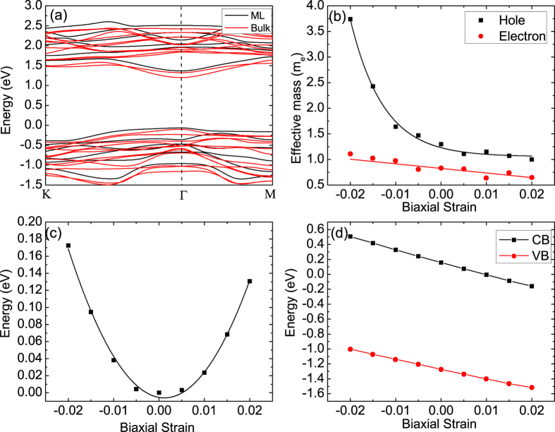
The optimized ReS2 unitcell, which exhibits in a distorted octahedral layer structure with triclinic symmetry, is shown in Fig. 1. The calculated lattice constants are a = 6.51 Å, b = 6.41 Å, and c = 6.46 Å, respectively. These calculated lattice constants are in good agreement with experimental values (a = 6.45 Å, b = 6.39 Å, and c = 6.40)17. They are also exactly the same as the theoretical results reported by Tongay et al. (a = 6.51 Å, b = 6.41 Å)12. The S-Re bond length, Re-Re distance and S-S distance in one layer are 2.43/2.37 Å, 2.81 Å, and 2.88/3.25 Å, respectively. Note that the two values of S-Re bond length and S-S distance are due to the slight lattice distortion of S atoms in bulk ReS2. Hence, ReS2 has a unique crystal structure, which is distinctively different from other TMDs, in which their graphene-like hexagonal crystal structure is composed of layers of metal atoms sandwiched between layers of chalcogen atoms. From Fig. 2a, it is seen that bulk ReS2 is a direct gap semiconductor with a bandgap of 1.30 eV, which is close to the experimental value of 1.32 eV18. Based on the optimized lattice constants of bulk ReS2, we increase the interlayer spacing c to 20 Å to build a ML ReS2 model. It is found that the optimized lattice constants of ML ReS2 are a = 6.51 Å and b = 6.41 Å, which are exactly the same as the bulk. The same optimized lattice constants of bulk and ML ReS2 indicate that the interlayer coupling is negligible. This issue will be discussed in details later. The calculated band structure of ML ReS2 is shown in Fig. 2a. It is seen that ML ReS2 also shows a direct gap semiconductor characteristic with a bandgap of 1.43 eV, which is exactly the same as recently reported value12. It is worth noting that the nature of band structure of ReS2 is independent of the number of layer, which is in strong contrast to other TMDs, such as MoS2 and WS2, in which the nature of their band structures is strongly dependent on the number of layers6.
Figure 1. Top view (a) and side view (b) of the crystalline structures of distorted-1T (1Td) phases of ReS2 monolayer.
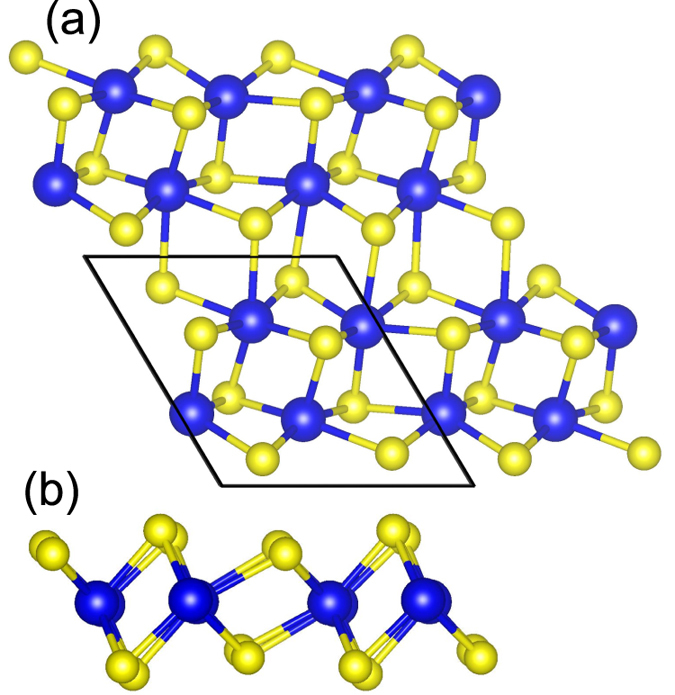
Blue balls represent Re atoms and yellow balls represent S atoms.
Figure 2.
(a) Calculated band structures of ML (black) and bulk ReS2 (red). (b) Variation of electron (red) and hole (black) effective masses with biaxial strain in ML ReS2. (c) Variation of relative energy with biaxial strain in ML ReS2. Here, we set the relative energy of the free strain system is zero. (d) Band edge shift as a function of biaxial strain in ML ReS2.
In order to confirm the weak interlayer coupling, we further calculate the formation enthalpies of bulk and ML ReS2, ΔEf, using following equation:
 |
where  is the total energy of the bulk and ML ReS2, μRe,(S) denotes the corresponding atomic chemical potential calculated from metallic Re or solid S unitcell, respectively. In the calculation, we neglect the entropy contribution at 0 K. It should be noted that the calculated formation enthalpies of bulk and ML ReS2 are nearly identical (1.69 eV per ReS2 unit). Our DFT calculations without considering van der Waals (vdW) correction indeed confirm the weak interlayer coupling with the coupling energy of only 7 meV per unitcell, which is slightly smaller than the reported value of 18 meV12. It should be noted that the reported value of 18 meV was also calculated without vdW correction. We further calculate the interlayer coupling energy considering vdW correction by employing optB88-vdW functional, the calculated interlayer coupling energy is 0.265 eV. The difference of the interlayer coupling energy shows that vdW correction plays an important role in the theoretical calculation on multi-layer 2D materials19. In order to further verify the weak interlayer coupling, a more appropriate quantity to analyse is the surface energy for the exfoliation of the monolayer, Ef which is defined as
  , where S is the surface area of ML ReS2 unitcell and EML,bulk is the energy of ML and bulk ReS2 unitcell, respectively. NL is the number of layers in each bulk ReS2 unitcell, in which, there are two layers in ReS2 unitcell. The calculated energy is 3.46 × 10⁻⁴ or 0.098 eV/Å2 without or with vdW correction, respectively. The low coupling energy and surface energy for the exfoliation of the monolayer indicate that single layer ReS2 can be easily exfoliated from the bulk12.
Electronic structure and acoustic phonon-limited charge carrier mobility in ML ReS2
It is well-known that in inorganic semiconductor, the coherent wavelength of thermally activated electrons or holes at room temperature is much larger than lattice constants and is nearly equal to that of acoustic phonon modes in the center of first Brillouin zone (FBZ). Since the electron-acoustic phonon coupling dominates the scattering at the low energy regime20,21, the charge carrier mobility can be calculated by the deformation potential (DP), which has been extensively applied to calculate the mobility of 2D materials22. Based on the DP theory, the charge carrier mobility can be obtained by using the following formula23,24:
 |
where m* is the effective mass and T is the temperature, E1 is the DP constant which is defined as the shift of the band edges induced by strain, and C is the elastic modulus of uniformly deformed crystal under strain. For a 2D material, the in-plane stiffness C is defined as  , where E is the total energy of layered supercell, δ is the applied biaxial strain and S0 is the area of the optimized supercell. The effective mass m* for charge transport is calculated by
  . All the above mentioned parameters can be obtained from our DFT calculations. In this study, only biaxial strains (including both compressive and tensile strains) are considered. The calculated electronic properties of ML ReS2 varying with strain are shown in Fig. 2b–d.
Stability and edge energy of ReS2 NRs
ReS2 NRs can be directly produced by cutting ML ReS2 along x or y direction (see Supplementary Fig. S1 online), namely, RX-series or RY-series, respectively. First, we try to explore the stability of ReS2 NRs and figure out their energetically favorable configuration. It should be noted that no chemical functionalization, such as hydrogenation at the edges, is considered in this study although it was reported that hydrogenation at NR edges can make NRs more stable11.
For RY-series and RX-series, we select 5 different NR terminals and calculate their ground-state energies through optimizing structures by constraining the NR length in one unitcell. The distance between NR and its neighboring images is set to 18 Å and period boundary conditions (PBCs) are employed. Calculations on NRs with and without spin polarization are carried out to investigate the magnetic properties and the structure stability. According to the calculated density of states (DOS) (see Supplementary Fig. S2 online). It is seen that the calculated magnetic moments are zero for all selective NRs and the ground-state energies with and without spin polarization are identical. Accordingly, we only discuss the results without spin polarization in the following study. For comparison, it should be noted that zigzag-edge WS2 and MoS2 NRs are metallic and ferromagnetic11,25.
The edge energy (Eedge) is an indication of the NR’s stability, and can be calculated based on:
 |
where ERB is the total energy of the ReS2 NR, and  is the energy of ReS2 unitcell calculated from the monolayer. L is the length of NRs. nS,(Re) is the number of extra S or Re atoms at the edges, respectively. μS,(Re) is the chemical potentials of S or Re, respectively. It should be noted that the chemical potentials of Re and S are decided by the thermodynamics condition. For ReS2, at equilibrium, we have
  , where
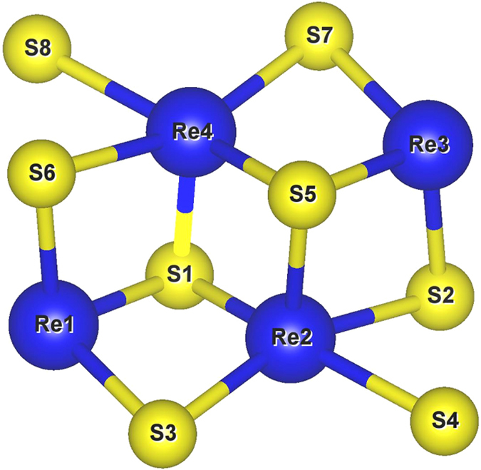
  is the chemical potential of ReS226. The calculated edge energies of bare NRs as well as 3D view of their corresponding NR configurations are shown in Fig. 3. It is seen that RY-S8Re4 has the minimum edge energy. Consequently, we only focus on exploring the electronic properties of RY-S8Re4 NR. The optimized structure of RY-S8Re4 NR is shown in Fig. 4.
Figure 3. The calculated edge energies of different types of ReS2 NRs.
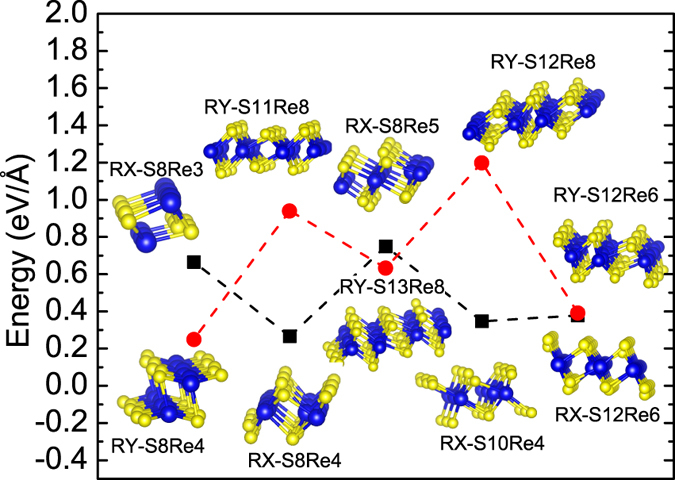
Figure 4. The optimized model of RY-S8Re4 NR unitcell.
Size-dependent band structure of nanoribbions
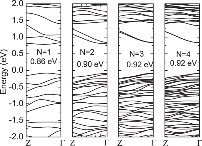
Beyond ML ReS2, the electronic properties of ReS2 NRs remain largely unexplored, which are crucial for their applications in nanodevices. Here, we focus on the size effect on their electronic properties. It is well-known that NRs (1D) have different electronic properties compared to mono- or multi-layer (2D) form. The edge atoms of NRs introduce new flat energy levels at both valence and conduction band edges, narrowing the band gap accordingly. Here, we further investigate the quantum size effect on the bandgap of ReS2 NRs (RY1-series). Our calculation results show that RY1-NRs are semiconductors with a director bandgap, and the bandgap increases with increasing ribbon width (N), and converges to 0.92 eV as shown in Fig. 5. In our models, N = 1, 2, 3, and 4 corresponds to a width of 13.27, 18.27, 20.58, 26.40 and 38.19 Å, respectively. It should be noted that for N = 1, which corresponds to a RY1-NR with a width of 13.27 Å, the k-space conduction band minimum and valence band maximum shift away from Γ point. But the NR still retains the nature of direct bandgap, which may be caused by the narrow width and symmetry-breaking in the FBZ.
Figure 5. The calculated results of size-dependent band structure of RY1-NRs.
Discussion
Figure 2b shows the variation of electron and hole effective masses with biaxial strain in ML ReS2 obtained from the DFT calculation results of strain-dependent band structure (see Supplementary Fig. S3 online). The calculated effective masses of electron and hole for strain-free ReS2 are 0.83 me and 1.30 me, respectively. These values are higher than those of MoS2, in which the effective mass for electron is 0.48 me and for hole is 0.60 me10. From our calculation results as shown in Fig. 2b, we find that electron effective mass is nearly strain-independent, with a value at about 0.83 me, corresponding to the strain-free state. Figure 2c shows the variation of total energy with biaxial strain. The in-plane stiffness C is calculated using Eq. 2 by fitting the energy–strain curve as shown in Fig. 2c and the value C is found to be 353.63 N/m. Figure 2d shows the shift of band edges as a function of biaxial strain. The DP constants E1 are calculate as dEedge/dδ, equivalent to the slope of the fitting lines as shown in Fig. 2c, where Eedge is the energy of conduction or valence band edge, and δ is the applied strain. The calculated DF constants for electron and hole are −15.17 and −9.5, respectively. We notice that the absolute values of DP constants in ReS2 are higher than those in MoS2 (~−11 for electron and ~−5 eV for hole10, respectively). According to the definition of DP, a higher absolute value of DP constant indicates a more strain-dependent band edge shift. Hence at the same strain level, the band edge shift of ReS2 is larger than that of MoS2. It should be noted that the band edge shift is not equivalent to the bandgap change. Our calculations show that the bandgap is 1.51 eV at −2% compressive strain and reduces to 1.35 eV at 2% tensile strain. Thus the bandgap difference is only 0.16 eV from −2% compressive to 2% tensile strain (see Supplementary Fig. S4 online). Since the bandgap of monolayer ReS2 is insensitive to strain, therefore, ReS2 is suitable for flexible electronic device applications.
Based on the obtained values of E1, C, and m*, and also Eq. 2, the acoustic phonon-limited charge carrier mobilities of electron and hole at room temperature (T = 300 K) are calculated and listed in Table 1. It is seen that the calculated electron and hole mobilities are 34.21 and 31.09 cm2/Vs, respectively. Hence the electron and hole mobilities are very close to each other in ML ReS2. Currently, there are no experimental results on the charge carrier mobilities of ML ReS2. However, the experimental result of electron mobility in bulk ReS2 at room temperature was reported to be 19 cm2/Vs27. In general, a ML TMD has a lower electron mobility than its bulk counterpart. For example, the bulk MoS2 mobility is as high as 200–500 cm2/Vs28, but the mobility of ML MoS2 is only in the range of 0.1–10 cm2/Vs29,30. The low mobility of ML MoS2 may potentially limit its applications in practical devices. Although the underlying reason for the reduced mobility of ML MoS2 was explained by using the Coulomb scattering model31, other mechanisms, such as quantum confinement, defect scattering and substrate effect, may also play an important role in mobility reduction. Currently, how to increase the charge carrier mobility of ML MoS2 is still a challenge.
Table 1. Deformation potential E1, in-plane stiffness C, effective mass m*, and mobility μ for electron (e) and hole (h) in ML ReS2 at 300 K.
| carrier type | E1(eV) | C(N/m) | m*(me) | μ (cm2/Vs) |
|---|---|---|---|---|
| e | 15.17 | 353.63 | 0.8 | 34.21 |
| h | 9.5 | 353.63 | 1.34 | 33.04 |
In our study, both bulk and monolayer ReS2 forms possess a direct bandgap characteristic and the calculated bandgap of 1.30 eV for bulk ReS2 is only slightly lower than that of 1.43 eV for monolayer ReS2 as shown in Fig. 2a. The unchanged bandgap characteristic and the small difference in bandgap energy between bulk and monolayer forms clearly indicate that the van der Waals interlayer interaction is weak. Hence the band structure of ReS2 is nearly independent of the number of layers. From our calculation results as shown in Fig. 2, it is seen that ML ReS2 has nearly the same mobility as its bulk counterpart. This nearly identical mobility in ML and bulk ReS2 may be due to the weak interlayer coupling in ReS212. Hence, it is expected that ReS2 may be more advantageous than other TMDs for making 2D materials-based nanodevices. It is worth noting that our theoretical calculations for mobility are based on perfect ML ReS2 without considering any intrinsic or extrinsic defects. In practical fabrication process, native defects such as S vacancies may exist in samples, which can increase free carrier concentration as well as elastic scattering. Hence, the real samples may have a lower mobility than the theoretically predicted value. However, the mobility of ML may be recovered through using high-k dielectric. For example, recently, the mobility ML MoS2 covered by a high-k dielectric layer and metal topgate was reported as high as 900 cm2/Vs for ML MoS231.
The optimized structure of RY-S8Re4 NR is shown in Fig. 4, in which we find that the zigzag edge of RY-S8Re4 is terminated by S-Re-S atoms (Re-centered-S). The edge termination of the most stable ReS2 NR is different compared to other TMD-based NRs, such as MoS2 NRs, in which S-terminated zigzag NRs are the most stable without hydrogen saturation11. The optimized bond lengths between two nearest atoms in RY-S8Re4 NR are shown in Table 2. For comparison, the optimized bond lengths between two nearest atoms in ML ReS2 are shown in brackets. Interestingly, we find that the bond lengths between two nearest atoms in RY-S8Re4 NR are slightly longer than those in ML ReS2. No significant distortion is found in the structure optimization of RY-S8Re4 NR.
Table 2. The optimized bonding lengths in Å between two nearest atoms in RY-S8Re4 NR as shown in Fig. 4.
| S1 | S2 | S3 | S4 | S5 | S6 | S7 | S8 | |
|---|---|---|---|---|---|---|---|---|
| Re1 | 2.38(2.37) | NA | 2.42(2.39) | NA | NA | 2.36(2.33) | NA | NA |
| Re2 | 2.39(2.37) | 2.45(2.43) | 2.41(2.39) | 2.49(2.45) | 2.38(2.36) | NA | NA | NA |
| Re3 | NA | 2.36(2.33) | NA | NA | 2.38(2.36) | NA | 2.42(2.39) | NA |
| Re4 | 2.45(2.43) | NA | NA | NA | 2.39(2.37) | 2.45(2.43) | 2.41(2.39) | 2.49(2.45) |
For comparison, the corresponding bond lengths in ML ReS2 are shown in brackets.
The weak distortion and high stability of RY-S8Re4 NR are due to its unique structure: ReS2 has the distorted CdCl2-type layer structure, with each Re atom bonding with 6S atoms, forming an octahedral complex (ReS6) as shown in the inset of Fig. 6. The slight increase in bond length along the six directions and odd valence electrons from Re (5d56s2) may result in the elongated Jahn-Teller distortions when degeneracy is broken. The d7 electronic configuration of Re provides one electron in the two degenerate eg orbitals ( and
and  ), which involve in the degeneracy point directly at S, leading to doubly degenerate electronic ground states. Hence, a distortion may further enhance an energetic stability, which can be proved by analyzing the projected density of states (PDOS) in RY-S8Re4 NR as shown in Fig. 6. It is seen that Re-dxy and
  orbitals have significant overlap with S-p orbitals. When such an elongation occurs in ReS2 NRs, this may push the antibonding orbital Re-
 to a higher energy level and bonding orbitals Re-dxz and/or Re-
 to a lower energy level, causing ReS2 NRs to be more energetically stable. In contrast to other TMDs-based NRs, such as MoS2 NRs, it was reported that a large distortion was found in edges during the structure optimization even using hydrogen saturation11.
Figure 6. The calculated projected density of states of RY-S8Re4 NR.
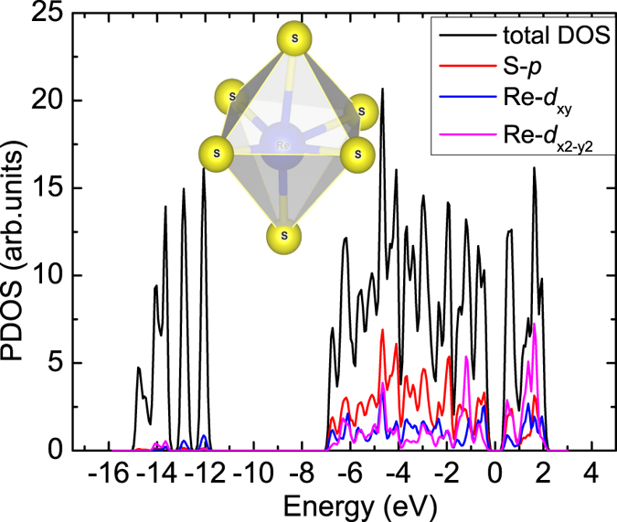
The inset is the ReS6 octahedral complex.
Quantum size effects on band structure of ReS2 NRs are shown in Fig. 5. Interestingly, the direct bandgap of ReS2 NRs finally converges to 0.92 eV in contrast to ML ReS2 bandgap of (1.43 eV), which shows that the bandgap of ReS2 NR is less strongly dependent on the width than that of other layered TMDs. Compared with other TMD-based NRs, such as MoS2 NRs, the bandgap finally converges to 0.56 eV16, which is much smaller than their monolayer counterpart (1.90 eV)32. Besides, the bandgap of MoSe2 NRs with armchair edges reduces to 0.38 eV from their monolayer value 1.55 eV33. In some extreme cases, TMD NRs may even show metallic behavior11,16. Clearly, for ReS2 NRs, the reduction in the bandgap compared to the monolayer value is much smaller than other TMDs NRs. It is known that the reduced bandgap may limit the applications of TMDs in electronic nanodevices, especially in optoelectronics, in which the nature and the magnitude of bandgap play critical roles in devices. Hence, we consider that ReS2 NRs have more stable structure and more robust direct bandgap characteristic, thus ideal for applications in optoelectronic nanodevices.
In conclusion, we have studied the electronic properties of ML, multilayer and NR forms of ReS2. In contrast to other TMDs, ML ReS2 has similar behavior as its bulk due to interlayer electronic and vibrational decoupling. We also calculate the mobilities of electron and hole in ML ReS2 and find that the mobilities of ML and bulk ReS2 are comparable, which is in strong contrast to other TMDs in which a drastic reduction in mobilities from bulk to ML form is often observed. Moreover, we also investigate the quantum size effect on the bandgap of ReS2 NRs and find the bandgap is weakly dependent on the NR width, and converges to 0.92 eV for wide NRs. Our work suggests that ReS2, with robust sizable and direct bandgap semiconducting characteristics, is a promising material suitable for TMD-based optoelectronic nanodevices.
Methods
All calculations were carried out using the density functional theory (DFT) with the generalized gradient approximation (PBE-GGA)34 and the projector augmented-wave (PAW) pseudopotential plane-wave method35, as implemented in the VASP code36. For the PAW pseudopotential, we included 5d5 and 6s2 valence for Re; for S, the n = 3 shell is included as valence (3s2 and 3p4). A 10 × 10 × 1 Monkhorst-Pack k-point grid was used for monolayered unitcell geometry optimization calculations and a plane-wave basis set with an energy cutoff of 500 eV. A 8 × 1 × 1 grid for k-point sampling in geometry optimization was consistently used for NRs in our calculations. Good convergence was obtained with these parameters and the total energy was converged to 1.0 × 10⁻⁵ eV per atom, as well as edge energy was converged to 1.0 × 10⁻³ eV/Å. For the interlayer coupling energy calculation, we carried out comparative calculations both with and without the van deer Waals correction by employing optB88-vdW functional37. In order to discuss the spin polarization effect on the electrical properties of NRs, calculations both with and without spin polarization were carried out to investigate the magnetic properties of the nanoribbons.
Additional Information
How to cite this article: Yu, Z. G. et al. Robust Direct Bandgap Characteristics of One- and Two-Dimensional ReS2. Sci. Rep. 5, 13783; doi: 10.1038/srep13783 (2015).
Supplementary Material
Acknowledgments
This research was sponsored by the Agency for Science, Technology and Research (A*STAR) and computational resource was provided by A*STAR Computational Resource Centre, Singapore (ACRC).
Footnotes
Author Contributions Z.G.Y. and Y.-W.Z. wrote the main manuscript text and prepared all figures. Z.G.Y. and Y.-W.Z. have contributed equally to this work. Electron and hole mobility calculations were carried out by Y.C. All authors reviewed the manuscript.
References
- Butler S. Z. et al. Progress, Challenges, and Opportunities in Two-Dimensional Materials Beyond Graphene. ACS Nano 7, 2898–2926 (2013). [DOI] [PubMed] [Google Scholar]
- Lopez-Sanchez O., Lembke D., Kayci M., Radenovic A. & Kis A. Ultrasensitive photodetectors based on monolayer MoS2. Nat. Nanotechnol. 8, 497–501 (2013). [DOI] [PubMed] [Google Scholar]
- Baugher B. W. H., Churchill H. O. H., Yang Y. & Jarillo-Herrero P. Optoelectronic devices based on electrically tunable p-n diodes in a monolayer dichalcogenide. Nat. Nanotechnol. 9, 262–267 (2014). [DOI] [PubMed] [Google Scholar]
- Pospischil A., Furchi M. M. & Mueller T. Solar-energy conversion and light emission in an atomic monolayer p-n diode. Nat. Nanotechnol. 9, 257–261 (2014). [DOI] [PubMed] [Google Scholar]
- Ross J. S. et al. Electrically tunable excitonic light-emitting diodes based on monolayer WSe2 p-n junctions. Nat. Nanotechnol. 9, 268–272 (2014). [DOI] [PubMed] [Google Scholar]
- Yun W. S., Han S. W., Hong S. C., Kim I. G. & Lee J. D. Thickness and strain effects on electronic structures of transition metal dichalcogenides: 2H-MX2 semiconductors (M = Mo, W, X = S, Se, Te). Phys. Rev. B 85, 033305 (2012). [Google Scholar]
- Geim A. K. & Grigorieva I. V. Van der Waals heterostructures. Nature 499, 419–425 (2013). [DOI] [PubMed] [Google Scholar]
- Zhang H., Li X. & Liu L. Tunable electronic and magnetic properties of WS2 nanoribbons. J. App. Phys. 114, 093710 (2013). [Google Scholar]
- Tongay S., Varnoosfaderani S. S., Appleton B. R., Wu J. & Hebard A. F. Magnetic properties of MoS2: Existence of ferromagnetism, Appl. Phys. Lett. 101, 123105 (2012). [Google Scholar]
- Cai Y., Zhang G. & Zhang Y.-W. Polarity-reversed robust carrier mobility in monolayer MoS2 nanoribbons. J. Am. Chem. Soc. 136, 6269–6275 (2014). [DOI] [PubMed] [Google Scholar]
- Pan H. & Zhang Y.-W. Edge-dependent structural, electronic and magnetic properties of MoS2 nanoribbons. J. Mater. Chem. 22, 7280 (2012). [Google Scholar]
- Tongay S. et al. Monolayer behaviour in bulk MoS2 due to electronic and vibrational decoupling. Nature commun. 5, 3252–3257 (2014). [DOI] [PubMed] [Google Scholar]
- Fujita T. et al. Chemically exfoliated MoS2 nanosheets. Nanoscale 6, 12458–12462 (2014). [DOI] [PubMed] [Google Scholar]
- Ataca C., Sahin H., Aktürk E. & Ciraci S. Mechanical and electronic properties of MoS2 nanoribbons and their defects. J. Phys. Chem. C 115, 3934–3941 (2011). [Google Scholar]
- Botello-Méndez A. R., López-Urías F., Terrones M. & Terrones H. Metallic and ferromagnetic edges in molybdenum disulfide nanoribbons. Nanotechnology 20, 325703 (2009). [DOI] [PubMed] [Google Scholar]
- Li Y., Zhou Z., Zhang S. B. & Chen Z. MoS2 Nanoribbons: High stability and unusual electronic and magnetic properties. J. Am. Chem. Soc. 130, 16739–16744 (2008). [DOI] [PubMed] [Google Scholar]
- Ho C. H., Huang Y. S., Liao P. C. & Tiong K. K. Crystal structure and band-edge transitions of ReS2−xSex layered compounds. J. Phys. Chem. Solids 60, 1797–1804 (1999). [Google Scholar]
- Marzik J. V., Kershaw R. & Dwight K. Photoelectronic properties of MoS2 and MoSe2 single crystals. J. Solid State Chem. 51, 170–175 (1984). [Google Scholar]
- Björkman T., Gulans A., Krasheninnikov A. V. & Nieminen R. M. van der Waals bonding in layered compounds from advanced density-functional first-principles calculations. Phys. Rev. Lett. 108, 235502 (2012). [DOI] [PubMed] [Google Scholar]
- Kaasbjerg K., Thygesen K. S. & Jacobsen K. W. Phonon-limited mobility in n-type single-layer MoS2 from first principles. Phys. Rev. B 85, 115317 (2012). [Google Scholar]
- Kaasbjerg K., Thygesen K. S. & Jauho A.-P. Acoustic phonon limited mobility in two-dimensional semiconductors: Deformation potential and piezoelectric scattering in monolayer MoS2 from first principles. Phys. Rev. B 87, 235312 (2013). [Google Scholar]
- Bardeen J. & Shockley W. Deformation potentials and mobilities in non-polar crystals. Phys. Rev. 80, 72–80 (1950). [Google Scholar]
- Price P. Two-dimensional electron transport in semiconductor layers. I. Phonon scattering. J. Ann. Phys. 133, 217–239 (1981). [Google Scholar]
- Xi J., Long M., Tang L., Wang D. & Shuai Z. First-principles prediction of charge mobility in carbon and organic nanomaterials. Nanoscale 4, 4348–4369 (2012). [DOI] [PubMed] [Google Scholar]
- Ouyang F. et al. Effects of edge hydrogenation on structural stability, electronic, and magnetic properties of WS2 nanoribbons. J. Appl. Phys. 114, 213701 (2013). [Google Scholar]
- Schweiger H., Raybaud P. Kresse G. & Toulhoat H. Shape and edge sites modifications of MoS2 catalytic nanoparticles induced by working conditions: A theoretical study. J. Catal. 207, 76–87 (2002). [Google Scholar]
- Tiong K. K., Ho C. H. & Huang Y. S. The electrical transport properties of MoS2 and MoSe2 layered crystals. Solid State commun. 111, 635–640 (1999). [Google Scholar]
- Fivaz R. & Mooser E. Mobility of charge carriers in semiconducting layer structures. Phys. Rev. B 163, 743 (1967). [Google Scholar]
- Novoselov K. S. et al. Two-dimensional atomic crystals. Proc. Natl. Acad. Sci. USA 102, 10451–10453 (2005). [DOI] [PMC free article] [PubMed] [Google Scholar]
- Ayari A., Cobas E., Ogundadegbe O. & Fuhrer M. S. Realization and electrical characterization of ultrathin crystals of layered transition-metal dichalcogenides. J. Appl Phys. 101, 014507 (2007). [Google Scholar]
- Radisavljevic B., Whitwick M. B. & Kis A. Integrated circuits and logic operations based on single-layer MoS2. ACS Nano 5, 9934–9938 (2011). [DOI] [PubMed] [Google Scholar]
- Mak K. F., Lee C., Hone J., Shan J. & Heinz T. F. Atomically thin MoS2: A new direct-gap semiconductor. Phys. Rev. Lett. 105, 136805 (2010). [DOI] [PubMed] [Google Scholar]
- Tongay S. et al. Thermally driven crossover from indirect toward direct bandgap in 2D semiconductors: MoSe2 versus MoS2. Nano Lett. 12, 5576–5580 (2012). [DOI] [PubMed] [Google Scholar]
- Perdew J. P., Burke K. & Ernzerhof M. Generalized gradient approximation made simple. Phys. Rev. lett. 77, 3865 (1996). [DOI] [PubMed] [Google Scholar]
- Blöchl P. E. Projector augmented-wave method. Phys. Rev. B 50, 17953 (1994). [DOI] [PubMed] [Google Scholar]
- Kresse G. & Furthmüller J. Efficiency of ab-initio total energy calculations for metals and semiconductors using a plane-wave basis set. J. Comput. Mater. Sci. 6, 15 (1996). [DOI] [PubMed] [Google Scholar]
- Klimeš J., Bowler D. R. & Michealides A. Van der Waals density functionals applied to solids. Phys. Rev. B 83, 195131 (2011). [Google Scholar]
Associated Data
This section collects any data citations, data availability statements, or supplementary materials included in this article.


