

Significance
We demonstrate that, instead of the charge generation mechanism, charge collection can readily explain the bottleneck toward higher efficiency single organic semiconductor based OPVs (SS-OPVs). This change in archetype has the potential to transform the design rules for materials used in OPV devices and would inspire searches for a completely different set of polymers for OPV cells. Furthermore, we believe that our findings will broaden the understanding of the physics of charge transport and the impact of charged defect states in organic electronic devices. Hence, this work should have deep and immediate impact on the chemists, materials scientists, and device physicists in the field and would be of broad interest to the organic electronics community.
Keywords: exciton, charge collection, organic photovoltaic, solar cell, organic defects
Abstract
The bulk heterojunction (BHJ) organic photovoltaic (OPV) architecture has dominated the literature due to its ability to be implemented in devices with relatively high efficiency values. However, a simpler device architecture based on a single organic semiconductor (SS-OPV) offers several advantages: it obviates the need to control the highly system-dependent nanoscale BHJ morphology, and therefore, would allow the use of broader range of organic semiconductors. Unfortunately, the photocurrent in standard SS-OPV devices is typically very low, which generally is attributed to inefficient charge separation of the photogenerated excitons. Here we show that the short-circuit current density from SS-OPV devices can be enhanced significantly (∼100-fold) through the use of inverted device configurations, relative to a standard OPV device architecture. This result suggests that charge generation may not be the performance bottleneck in OPV device operation. Instead, poor charge collection, caused by defect-induced electric field screening, is most likely the primary performance bottleneck in regular-geometry SS-OPV cells. We justify this hypothesis by: (i) detailed numerical simulations, (ii) electrical characterization experiments of functional SS-OPV devices using multiple polymers as active layer materials, and (iii) impedance spectroscopy measurements. Furthermore, we show that the collection-limited photocurrent theory consistently interprets typical characteristics of regular SS-OPV devices. These insights should encourage the design and OPV implementation of high-purity, high-mobility polymers, and other soft materials that have shown promise in organic field-effect transistor applications, but have not performed well in BHJ OPV devices, wherein they adopt less-than-ideal nanostructures when blended with electron-accepting materials.
The photovoltaic properties of semiconducting polymers arranged in a simple metal–polymer–metal sandwich structure were first demonstrated in 1993 by several groups (1–3). The efficiency values of these early photovoltaic (PV) cells were minuscule mainly because of the poor short-circuit current densities ( ∼10 µA cm−2) under standard 1 sun illumination. By definition,
| [1] |
where is the voltage-dependent photocurrent, is the exciton diffusion-dissociation (or free-charge generation) efficiency, is the charge (free-carrier) collection efficiency, and is the maximum current density obtained by integrating absorption spectra ( mA cm−2 for typical semi-conducting polymers). The difference between and was attributed to an inefficient (<0.1%) arising from ultrashort exciton diffusion lengths (∼10–15 nm) in semiconducting polymers and was eventually interpreted by Onsager's theory of geminate pair recombination (4–6). This classical interpretation assumes, on the other hand, that .
To improve , Heeger and co-workers (7) and Holmes and co-workers (8) introduced the concept of bulk heterojunction (BHJ) devices in 1995. Here, the active layer consists of two organic semiconductors: an electron-donating, hole-conducting (p-type) semiconducting polymer blended with an electron-accepting, electron-conducting (n-type) organic semiconductor. It was suggested that the interpenetrating bicontinuous morphology creates a distributed p–n heterojunction throughout the absorbing semiconducting active layer. This heterojunction (HJ) between the electron-donating and electron-accepting materials is able to dissociate excitons before they recombine, and therefore one expects and observes a higher and an improved . Once the nanostructure of the donor–acceptor blend was optimized by controlling the casting solution, deposition protocols, and postprocessing conditions, the BHJ-OPV led to the highest-performing polymer-based OPV devices ever reported in the literature (9–13). In fact, a number of groups have achieved (14), implying nearly perfect exciton dissociation () and charge collection ).
It has long been recognized, however, that despite a high , a number of critical (and possibly fundamental) limitations of the BHJ concept will prevent the approach from ever achieving efficiency and reliability comparable to highly efficient inorganic solar cells. First, the energy band discontinuity ) at the HJ directly translates to an irretrievable loss of the open-circuit voltage, (15, 16), because electrons and holes recombine at the donor–acceptor interface (i.e., the cross-gap at the HJ) at energies lower than the optical gap of donor or acceptor (17). Second, the efficiencies of BHJ solar cells appear to be highly sensitive to the processing conditions [e.g., solution composition (18) and postprocessing annealing conditions (19)] and failure to achieve optimum morphology is reflected in very poor device efficiency (20, 21). Finally, because the activation energy of phase segregation is relatively small, the nanostructure continues to evolve (degrade) under standard operating conditions (22), shortening the useful lifetime of OPV technologies.
These fundamental limitations of BHJ-OPV devices suggest that the original SS-OPV concept should be reconsidered; specifically, the physical origin of the poor should be explained in much fuller detail. In this effort, we show that the main reason for poor in SS-OPV devices is the poor charge collection property () of the organic film. We establish this hypothesis by demonstrating a 100-fold improvement in of SS-OPV devices made of the commonly used semiconducting polymers poly[2-methoxy-5-(2-ethylhexyloxy)-1,4-phenylenevinylene] (MEH-PPV), poly(3-hexylthiophene) (P3HT), and poly[5,5′-bis(3-dodecyl-2-thienyl)-2,2’-bithiophene] (PQT-12) with inverted electrode configurations. This dramatic improvement in cannot be interpreted by the classical view of poor field-dependent in polymers. Furthermore, we used impedance spectroscopy and detailed optoelectronic numerical simulations to develop an alternate collection-limited model of OPV. The model allows us to reinterpret the classical experiments and help resolve a number of anomalous SS-OPV experiments (e.g., efficiency gain at lower intensity, voltage dependence of the reverse). Importantly, the numerical model, based exclusively on free-carrier transport, explains how the optoelectronic interplay defines the unconventional features in the external quantum efficiency (EQE) spectrum; indeed, the match between theory and experiments is remarkable. Bias-dependent EQE measurements further confirm a high rate of charge generation. Therefore, the proposed theory encourages the development of organic semiconductors with improved charge collection properties for highly efficient SS-OPVs. Such device configurations will ensure next-generation OPVs free of variability and/or reliability concerns associated with BHJ structures.
Key Experiment
The inverted device configuration has been studied widely for BHJ-OPV devices (23–25); however, its impact on SS-OPV cells has not been explored in full. Here, we perform a side-by-side comparison of the photovoltaic response for single polymer-based OPV devices with both the typical and inverted configurations. The device structures and the corresponding J-V characteristics (1 sun illumination) are shown in Fig. 1. This result establishes that there is a significant (∼200-fold) improvement in the photocurrent for the inverted device configuration relative to the standard OPV device configuration for an SS-OPV cell. The improvement is highly reproducible and has been observed routinely in the all of the devices fabricated.
Fig. 1.

(A) Device structure of the standard P3HT SS-OPV cell. (B) Energy band diagram of the absorbing layer, assuming MIM model (dashed line) vs. with band bending in the presence of charged defects (solid line). (C) Structure of the inverted SS-OPV with P3HT as the active material. (D and E) Corresponding J-V characteristics (under AM 1.5 illumination) of the standard and inverted devices, respectively.
Interpretation of the Key Experiment
We invoke the free-carrier–based collection theory to explain the origin of significant increase of in the inverted structure. Because the interchange of contacts affects charge collection efficiency, one must reexamine the presumption that by examining the field distribution within the polymer () and the alignment of the absorption and the collection zones ().
Defect-Induced Band Bending.
The energy bands of an OPV are frequently drawn assuming the metal–insulator–metal (MIM) model, where the active layer is modeled as defect-free intrinsic semiconductor (dashed lines of Fig. 1B) (26). In practice, the impedance spectroscopy data (see Fig. S1) indicate the presence of high density of defect states acting as p-type dopants in the semiconductor (27–30). Under solar illumination, these defects are filled by photoinduced electrons, and they form a space-charge region (with corresponding nonlinear bending of the energy band diagram) near the organic low work function metal (27) (the solid lines of Fig. 1B). The defect-induced band diagram associated with direct and inverted structures is shown in Fig. 2. The field screening associated with the defects divides the active region into space-charge and field-free regions. This nonlinear band diagram implies , according to the following rationale.
Fig. S1.

(A) C-V response of the P3HT photodiode under dark (blue) and light (red) measured at a low frequency (f = 200 Hz). (B) Corresponding MS plot for the C-V data. (C) C-f response of the same photodiode measured at V = 0 V. (D) Corresponding energy band diagram for the photodiode under light (red) and dark (blue). Note that the energy band diagrams are quite different under light and dark as confirmed by the C-V measurements. The deep level defects in the semiconducting polymer become filled under light, which increases the space-charge density in the device.
Fig. 2.

(A) Device structure and (B) energy bands of SS-OPV devices are shown with the standard architecture electrode and (C and D) the inverted electrode configurations. Note that the space-charge layer, or band bending, is located at the back-contact side in standard electrode devices, but it is moved to the front-contact side in the inverted devices. A more detailed, numerically calculated band diagram is shown in Fig. S2A. (E) Light absorption profiles from the front (Right) to the back (Left) contact is shown for both the standard and inverted electrode devices. Even though absorption is comparatively smaller for the inverted device, its photocurrent is higher due to improved charge collection. The charge collection zones are indicated by shaded regions in the figure. Clearly, inverted devices collect more due to the higher absorption at the front side of the contact.
Free-carrier transport in any semiconducting material can be described with the generalized drift-diffusion formalism. The electric field in the flat band region is negligible; therefore, charge transport in the field-free region is dictated exclusively by diffusion of the charges. The charge carrier mobility (or, alternatively, the charge carrier diffusion coefficient) in organic semiconductor is very low; therefore, the carrier diffusion length is small. This makes charge extraction from the neutral region highly inefficient. For example, the electron diffusion length in P3HT is estimated at , for an electron mobility and a typical recombination time . Due to such a low diffusion length, almost all of the photocarriers generated in the neutral region recombine before being collected by the electrodes. Conversely, charge collection in the space-charge region is enhanced greatly due to the presence of built-in electric field given by , where is the built-in voltage and is the length of the space-charge region. The electrostatic field drives the charge carriers by drift. This drift length is characterized by , which typically is limited by the space-charge length. Thus, the collection length in typical polymer film is given by
| [2] |
The corresponding defect-related collection efficiency, assuming uniform generation, is given by
| [3] |
In the Supporting Information (see Fig. S1), we show, by impedance spectroscopy measurements, that nm for a typical P3HT film and nm. Thus, Eq. 3 suggests that < 20%, for = 200 nm in P3HT.
Nonuniform Exciton Generation.
If the charge generation is spatially uniform, space-charge–limited collection itself does not explain the 100-fold difference in between the regular and the inverted structure. Indeed, and essentially are identical for both the structures because the intrinsic properties of the polymer do not depend on the position of the contacts. In addition, the for the two structures are comparable. The puzzle is resolved only when we use a standard numerical simulator to calculate the optical field profile inside the active region. Recall that semiconducting polymers generally are direct bandgap materials and, therefore, are strong absorbers of light. Most of the light is absorbed within the first few tens of nanometers of the film from the transparent contact of the cell. This is illustrated in Fig. 2E, where we plot the simulated absorption profile of P3HT photodiode for both standard and inverted electrode configurations (31).
With nonuniform generation, only those carriers generated within the space-charge region contribute to , and therefore Eq. 3 is rewritten as the following:
| [4] |
Here, is the average generation in the film at a distance from the contact that collects electrons.
In standard SS-OPV devices, the collection zone is located at the reflective-metal contact. This is because semiconducting polymers, being typically p-type, form the space-charge region at the contact with a work function nearer to vacuum (reflective-metal contact); unfortunately, the photogeneration at this back-contact is small. Thus, the collection efficiency given by Eq. 4 is very small, which explains the poor from an SS-OPV device using a regular architecture. Since all the OPV experiments in 1990s (1–3) utilized standard device configuration, the poor efficiency of SS-OPV is explained readily. In contrast, the peak of the spatial photogeneration and the charge-collection region are aligned for the inverted structure. The difference in explains the difference in , implying high charge carrier generation for these polymers.
To confirm that the increase in in the inverted SS-OPV structure is not specific to P3HT, we fabricated and characterized a series of inverted cells using other well-known organic semiconductors, such as MEH-PPV and PQT-12. The results, summarized in Figs. S3–S6, show that the inverted configuration consistently produce high comparable to P3HT, and their J-V responses and the EQE results can be simply and self-consistently explained by the collection-limited theory described above.
Fig. S3.
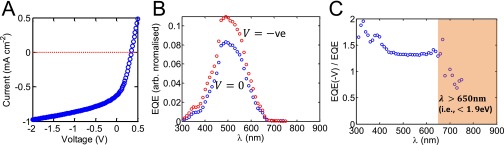
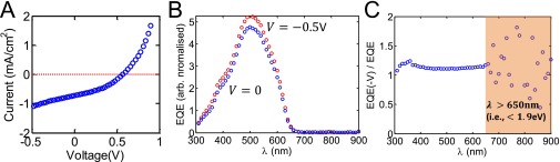
Experimentally obtained (A) J-V curve and (B) EQE spectrum at no applied bias (blue symbols) and EQE spectrum at a negative bias (V = −1 V) (red symbols) for the P3HT OPV device shown in Fig. S1A. (C) The ratio of EQE(V < 0)/EQE(V = 0). The EQE values for are very small and the ratio (in the shaded region) for this condition is not informative.
Fig. S6.
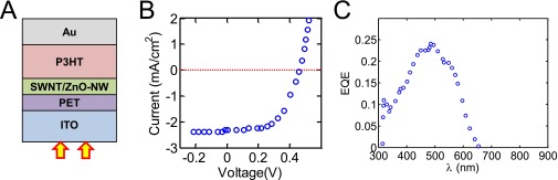
(A) Schematic of a P3HT photodiode from the literature (ref. 48). The structure in this case is ITO/PET/SWNT/ZnO /P3HT/Au. (B) Experimentally measured J-V relationship and the (C) experimentally measured EQE spectrum. Here, the substrate is poly(ethylene terephthalate) (PET) and the electrode was a combination of single-wall carbon nanotubes (SWNT) and zinc oxide nanowires (ZnO-NW).
Additional Explanation of Anomalous Results
High-Efficiency n-Type SS-OPV.
For an n-type semiconductor [e.g., [6,6]-phenyl-C61-butyric acid methyl ester (PCBM)], the space-charge region is formed at the hole collecting electrode (with a work function removed further from vacuum level), which is typically the transparent contact [i.e., indium-tin oxide (ITO), in most instances]. Thus, our theory predicts that the standard electrode configuration should lead to higher values in PCBM-only cells, and this prediction has recently been confirmed by several groups (32, 33). Interestingly, in PCBM-based SS-OPV devices (32, 33), the higher Jph is explained by considering free-carrier generation with the assumption that in fullerene-only films exciton binding energy is small (). Thus, our result on inverted P3HT-only devices confirms that free-carrier generation is significant even in the semiconducting polymer films and expands this paradigm of collection-limited theory of efficiency into a much broader regime.
Intensity-Dependent Efficiency Loss.
A distinguishing feature for OPV technologies is that their power conversion efficiencies improve at lower illumination intensity. Our proposed collection-limited theory of photocurrent offers a consistent explanation for this trend. In Fig. 3, we plot the normalized solar cell performance metrics as a function of illumination intensity. Current density values are normalized by the corresponding light intensity values.
Fig. 3.

Illumination intensity-dependent performance of organic solar cells. (A) Efficiency, (B) short-circuit current, (C) open-circuit voltage, and (D) FF as a function of illumination intensity. All of the performance metrics are normalized by performance values at intensity = 100 W cm−2. Symbols are experimental results obtained from ref. 29 for OPV devices and lines correspond to results from the self-consistent numerical simulations for typical inorganic solar cells.
Ideally, (normalized) and the fill factor (FF) should remain constant with intensity, because generation is proportional to light intensity. The open-circuit voltage (Voc) should increase slightly with intensity as the splitting of quasi-Fermi levels increases with light intensity. Thus, the overall efficiency should increase with intensity, as typically observed in all types of inorganic solar cells. However, as shown in Fig. 3, the (normalized) and FF of OPV cells decrease sharply with illumination intensity, which in turn reduces the efficiency.
These trends are consistent with the intensity-dependent charge collection efficiency model. In fact, by measuring the intensity-dependent capacitance–voltage (C-V) characteristics, one can determine the modulation of space-charge density and the corresponding change in collection lengths as a function of illumination intensity. In Fig. 4, we plot the measured C-V data as a function of illumination intensity for the same P3HT-based photodiode. From the slope of the Mott–Schottky plot (27), we find that the space-charge density increases with higher illumination intensity. This increase in space charge with illumination suggests that light illumination fills the deep level traps present in the polymeric semiconductor, and thereby increases the space-charge density (the full suite of impedance spectroscopy measurements is shown in the Supporting Information). Higher space-charge density screens the electric field within smaller length (LS), thereby reducing the collection efficiency (see Eq. 3, .
Fig. 4.

(A) Measured C-V data of the P3HT photodiode with an increasing intensity of incoming radiation. (B) Corresponding energy band diagram of the active layer of the device at low and high light intensities, as calculated using a self-consistent simulation model.
Voltage-Dependent Reverse Photocurrent.
Unlike BHJ-OPV cells, the of SS-OPV devices show a very strong voltage dependence, especially in the reverse bias regime (Fig. 5). It is argued that if the primary photoexcitation were free carriers, and if is assumed uniform throughout the absorber layer, ) should be field independent for negative voltages (5, 6, 34). Thus, a field-dependent is often referred to as an unambiguous signature for the exciton model, and generally explained by the voltage-dependent charge generation (or exciton dissociation) efficiency () (5, 6, 34).
Fig. 5.
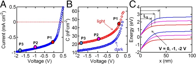
Origin of voltage-dependent photocurrent. (A) Measured light J-V characteristics for an inverted P3HT SS-OPV diode. P1, P2, and P3 are three representative points on the J-V curve. (B) Measured C-V characteristics of the same diode. (C) Corresponding energy band diagrams of the active layer of the device at various reverse biases highlighting the difference in Ls for points P1, P2, and P3 in the J-V response curve.
In Fig. 5, we provide a simpler explanation for the increase of in reverse bias, based on voltage-dependent collection efficiency (), and without invoking any rate-limiting role of excitons. Fig. 5A shows the J-V characteristics for an inverted P3HT-based photodiode for negative applied voltages. Clearly, the magnitude of the current density increases greatly in the negative voltages. Three representative points in the J-V plot are taken to explain such voltage dependence. Fig. 5C shows the active layer band diagram for these three different negative voltages obtained by numerical simulation. The plot illustrates the fact that the space-charge length increases under reverse bias. Because the charge collection length is limited by the space-charge length, , according to Eq. 3, the collection efficiency, , increases with negative voltages, explaining the increase in . The voltage-dependent modulation of is confirmed by the C-V measurement on the photodiode (Fig. 5B). The close agreement between the theory and experiment in Fig. 5 supports our assertion that the voltage-dependent charge collection can consistently interpret electrical performance of single-layer OPVs, and it does so without invoking any rate-limiting role of excitons.
Wavelength-Dependent Collection.
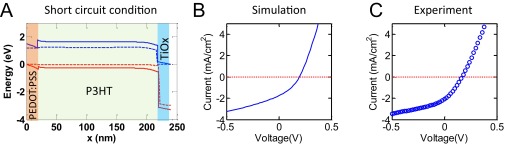
We have conducted a rigorous optoelectronic numerical study of the inverted P3HT photodiode structure to elucidate the wavelength-dependent carrier collection. In fact, we can reproduce the experimental EQE spectral features based on our model, as shown in Fig. 6. Fig. 6B compares the normalized EQE response obtained from experiments (circles) and simulations (solid line). Next, we will use the proposed theory to explain the wavelength-dependent EQE shape at four representative wavelength positions marked as P1, P2, P3, and P4 in Fig. 6B. The related carrier generation profiles (i.e., the calculated photon absorption profiles) are shown in Fig. 6C, and the numerically found absorption spectrum for the various layers is shown in Fig. 6A.
Fig. 6.

(A) Numerically calculated absorption spectrum for the various layers of the OPV structure. (B) Normalized EQE response measured from the experimentally fabricated OPV devices (circles) is compared with the normalized numerically calculated EQE (solid line). (C) Band diagram under short-circuit condition is shown (Top). Also, photogeneration (normalized to the number of incident photons) profiles are shown at four different wavelengths as marked in B.
For the case of point P4 ( nm), there is very little absorption in P3HT (Fig. 6 A and C), as a large portion of the absorption occurs in ITO and TiOx layers. Thus, the current, and hence the EQE, at this wavelength, is very low. Similarly for point P1, the low absorption near the band edge results in a low EQE.
The most interesting information, however, is obtained by comparing case P2 to case P3. The integrated absorption in the P3HT layers for case P3 ( nm) and case P2 ( nm) are comparable (Fig. 6A). The numerical simulation, however, suggests that whereas the integrated generation is similar, the spatial distributions are not. The photogeneration in the space-charge region for case P3 is higher compared with that of case P2, because a greater number of higher energy (i.e., shorter wavelength) photons are absorbed close to the interface inside the space-charge region. As a result, the collection-limited theory anticipates that the EQE for case P3 (shorter wavelength) would be significantly higher than that of case P2 (longer wavelength)––a prediction quantitatively validated by the measured EQE data shown in Fig. 6B. This result directly supports our collection-limited photocurrent model.
Discussion and Conclusions
We note that, in the inverted configuration, the TiOx buffer layer creates an organic–inorganic hybrid bilayer. It may be argued reasonably that the efficiency gain in the inverted HJ arises from efficient dissociation of the photogenerated excitons by the TiOx/polymer HJ. Here, we address this possibility with voltage-dependent EQE experiment and detailed numerical simulations to demonstrate that this is not necessarily the case. Fig. 7A shows EQE spectrum (at 0 V) (blue) and the EQE spectrum (at –1 V) (red) of the inverted P3HT-based SS-OPV device. The EQE(V = –1 V) is higher than the EQE(V = 0 V) for all wavelengths (i.e., carrier collection increases at all wavelengths for negative bias). However, the more informative value is the ratio of EQE(V = –1 V)/EQE(V = 0 V), as shown in Fig. 7B. Note that by taking the ratio, we eliminate the parasitic absorption in the layers other than P3HT, and we remove also the variable absorption for different wavelengths. This allows us to focus exclusively on the carrier collection. According to generation-limited theory, the collection is expected to improve for higher energy incident photons () as excitons at higher energies are more probable to be dissociated in the SS-OPV device. Remarkably, however, even at energies close to the band edge ∼1.9 eV (), the EQE ratio is comparable to those at significantly higher energies. The uniform enhancement in EQE with negative bias, represented by the EQE(V = –1 V)/EQE(V = 0 V) ratio for a large range of wavelengths (up to the band edge), supports the possibility of high exciton dissociation rate even close to the bandgap.
Fig. 7.

(A) Measured EQE (blue) and reverse-bias EQE(−V) (red) responses are shown. (B) The ratio of EQE(V = –1 V)/EQE(V = 0 V) is shown. The ratio near the band edge (1.9 eV) represents bias-dependent carrier collection of photogenerated carriers near the band edge. The ratio is high, indicating good exciton dissociation at these energy levels as well. The EQE values for λ > 650 nm are very small and the ratio (in the shaded region) for this condition is not informative. (C and D) Corresponding simulated results. The trends from experiments are captured in our exciton agnostic, transport-limited model.
Next, we provide three arguments supported by simulation results to further establish our hypothesis. First, we numerically simulate the photodiode response of Fig. 1 (Fig. S2) assuming only free-carrier transport without considering any role of TiOx in exciton dissociation. The simple fact that the (exciton-free) free-carrier response properly captures the shape and the magnitude of the J-V characteristics seen in experiments (Fig. 1), immediately, yet indirectly, suggests that one need not invoke the exciton dissociation at TiOx as a rate-limiting step. Second, the voltage-dependent modulation of electric field at the TiOx–P3HT interface is negligible (as most of the voltage drops across the depletion region due to electric field screening by the space charge); therefore, the strong voltage dependence of the photocurrent cannot be interpreted by field-dependent exciton dissociation at the TiOx–P3HT interface. Third, charge generation (or exciton dissociation) by the HJ should be proportional to the light intensity. However, Fig. 3 shows an efficiency loss at higher light intensity. Our collection-limited model consistently explains this observation.
Fig. S2.
Simulated (A) band diagram, and (B) J-V response for the ITO/TiOx/P3HT/PEDOT:PSS/Au structure. (C) The experimentally obtained J-V curve is reproduced here. (Note that we have not used any rate-limiting role of exciton dissociation in our simulation and still it explains the experimental observation.)
The collection-limited theory of photocurrent discussed in this paper does not contradict the well-known notion of exciton formation in polymers, especially characterized under monochromatic low-level illumination. Under the broadband solar illumination, however, the excess energy of the photons incident upon the polymer may be sufficient to dissociate excitons (35–38). Moreover, impurities or dopants in the bulk of the polymer may provide another channel for efficient exciton dissociation into free carriers. Second, our EQE measurements indicate the transport gap and optical gap for the polymers considered differ by <0.1 eV, explaining facile dissociation of excitons into free carriers. This result is consistent with previous transient photoconductivity results from Heeger and co-workers (37, 39), but differs substantially from those obtained from photophysical experiments, such as ultraviolet photoelectron spectroscopy (UPS)/inverse photoemission spectroscopy (IPES) (40). Therefore, the relevance of these photophysical experiments in interpreting device performance needs to be reconciled in future work on this topic. Finally, it may be possible that the charge-generation-limited theory, appropriately and broadly modified, may eventually explain the results we have presented. We simply suggest that the expansive experimental and computational results presented in this paper are consistently and collectively explained by a simple charge-transport-limited theory.
Finally, based on the transport-limited theory of OPV devices, we suggest that the role of the HJ in BHJ devices is to minimize the free-carrier recombination by keeping the electrons and the holes isolated in their respective electron acceptor and electron donor channels. This type-II staggered band strategy removes minority carriers, and thereby improves the effective carrier diffusion in their respective channels regardless of the defect density within the active region. Therefore, materials with high absorption across a broad spectral range and with high-mobility, ambipolar behavior would be ideal for single-semiconductor inverted OPV devices. This critical change in paradigm could greatly alter the design strategy of macromolecular chemists.
In summary, we have shown that inefficient charge extraction is the origin of low Jph in the standard SS-OPV device configuration. The charged defect states in the semiconductor screen the electric field within a few tens of nanometers of the electron-collecting contact, and thereby make charge extraction difficult. However, this extraction problem can be mitigated, in part, by the application of the correct electrode polarity relative to the incoming incident radiation for SS-OPV devices or by the insertion of closely spaced electrodes in the organic film (41). Therefore, our demonstration that charge extraction can be the key limiting step in these SS-OPV devices alters the molecular design considerations (e.g., highly crystalline, ambipolar polymers should be explored) of active layer polymers. In fact, these results suggest that several materials that are used in high-performance organic field-effect transistors could be implemented in OPV devices immediately as their miscibility and nanostructure with respect to an electron-accepting material (e.g., a fullerene derivative) are no longer of concern. In this way, the production of high-performance, reproducible, and long-lasting OPV devices could be on the near horizon.
Establishing the Energy Band Diagram of an Organic Photodiode
The energy bands of an organic photodiode are often drawn assuming the MIM model, where the active layer is considered as a defect-free, intrinsic semiconductor (Fig. 1A). Recent studies have found that semiconducting polymers contain a high density of electronic defect states, which act as p-type dopants (41–46). These defect states, especially those filled by electrons, form a space-charge region near the metal–organic interface. The space charge alters the electrostatics of the OPV device significantly by screening the electric field near the metal–organic junction. The resulting energy band diagram of the absorbing layer containing p-type defects is shown in Fig. 1B, which consists of two distinct regions. The first region is the space-charge region near the electron collecting contact. The space charge screens the electric field reflected as bending in energy bands. The second region is charge neutral, where the energy band is almost flat; in other words, the electric field in this region is negligibly small.
Impedance spectroscopy measurements are widely used to characterize the energy band diagram of semiconducting devices. In Fig. S1A, we plot the C-V response at a low frequency (200 Hz) for the P3HT photodiode (the device structure is shown in Fig. S1A, Inset). In the absence of space charge (or dopants), semiconducting polymers with wide bandgaps (i.e., eV) behave like insulating dielectric materials (i.e., Fig. 1A) and, as such, their capacitive responses should be similar to that of a parallel plate capacitor governed by the following equation:
| [S1] |
Here, is the dielectric constant of the polymer and is the thickness of the polymer layer. Clearly, CG is voltage independent. However, impedance measurements on organic photodiodes made of typical semiconducting polymers (e.g., P3HT and MEH-PPV) show strong voltage dependences. For example, Fig. S1A shows the response C-V characteristics for P3HT. This voltage-dependent C-V response invalidates the presumption of defect-free intrinsic band diagram (Fig. 1A) for organic photodiodes.
Next, we find that the measured C-V data for the P3HT photodiode exactly follow the Mott–Schottky (MS) equation (42, 46).
| [S2] |
Here, is the density of ionized dopants (or charged defect states) and is the built-in voltage. In Fig. S1B, the solid lines represent Eq. S2 and symbols are the measured data. The close agreement of the measured data with the MS equation attests to the formation of space-charge region near the metal–organic interface. The MS analysis, therefore, confirms the energy band diagram depicted in Fig. 1B for the P3HT photodiode. The corresponding space-charge (or ionized dopants/defects) density can be calculated from the slope of the MS plot, for which we find in the dark for the P3HT photodiode. Similar defect or dopant densities also have been reported previously by several groups (41–46). The reported space-charge densities are usually measured in the dark. In the following, we demonstrate that under light illumination increases significantly, which has a significant and profound impact on the charge collection in a photovoltaic device.
In Fig. S1, we show the measured C-V data under light illumination for the P3HT photodiode. We find capacitance increases significantly under illumination compared with the capacitance in the dark. The same MS analysis (Eq. S2) shows that the space-charge density under light is (Fig. S1B). This higher space-charge density implies a smaller , as evidenced from the following equation:
| [S3] |
For example, nm corresponding to at V, , and (typical numbers for P3HT photodiodes). A similar calculation under illumination shows for . This reduction in will be reflected in the energy band diagram, as shown in Fig. S1D. Clearly, the energy bands of the organic photodiode significantly change under light illumination, which has a dramatic impact on the charge collection efficiency as discussed in the main text (see Fig. 4B). Thus, it is critically important to understand the physics of and accurately estimate this device parameter.
To evaluate the accuracy of the estimation, in addition to C-V characteristics, we performed capacitance–frequency (C-f) measurements on the same P3HT photodiode both under dark and illumination conditions. These data are plotted in Fig. S1C. Note the unsaturated nature (or rising trend) of the C-f characteristics in the low-frequency regime for the measurement under illumination. Such unsaturated C-f characteristics provide a clear signature of light-induced filling of deep level traps (28, 47) and an associated increase in space-charge density. In addition, the unsaturated C-f characteristics imply that if the C-V measurements could be performed at lower frequencies, the estimated defect density would have been even higher. Thus, the calculated (light) from the slope of the MS plot (measured at 200 Hz, in Fig. S1B) is an underestimation of the actual space-charge density in the photodiode. In other words, the actual values of and the values of nm in a P3HT photodiode under light illumination. Even though many of the concepts on estimating are known in the literature and many groups have already published the values of in organic photodiodes (41–46), the consequences of this space-charge density on the device electrostatics or charge collection have not been, to our knowledge, discussed in full.
Numerical Simulation of Photocurrent
We have studied the transport characteristics of the free carriers numerically, including the poly(3,4-ethylene dioxythiophene) doped with poly(styrene sulfonate) (PEDOT:PSS)/P3HT/TiOx layers with appropriate bandgaps, electron affinities, and doping levels. We have assumed that (i) the TiOx layer is highly n-doped, (ii) the exciton dissociation is efficient/immediate, and (iii) the TiOx/P3HT interface plays no role in exciton dissociation. The calculated band diagram is shown in Fig. S2A. The simulated J-V curve (Fig. S2B) is consistent in detail with the experimentally measured J-V response (Fig. S2C).
Summary of Devices from Different Polymeric Semiconductors
Analysis of the P3HT Photoresponse.
The J-V relationship and the EQE spectrum for the P3HT-based inverted SS-OPV cell are shown in Fig. S3. The structure is that of ITO/TiOx/P3HT/Au. As discussed in the main text (see Fig. 7), the ratio of the bias-dependent EQE values shows no excitonic feature near the band edge. According to generation-limited theory of photocurrent, the collection is expected to improve for higher energy incident photons (), as excitons at higher energies are more likely to be dissociated into free carriers. However, even close to the band edge of ∼1.9 eV (), the collection has similar enhancement [i.e., the EQE(V < 0)/EQE(V = 0) ratio is ∼1.5 for almost the entirety of the wavelengths of light absorption]. This implies that the carriers are free even close to the band edge.
Experiments Involving Other Organic Semiconductors: The Case of PQT-12.
We have fabricated and tested these facts for another active layer material, namely PQT-12. The bandgap of PQT-12 is ∼1.9 eV, with an absorption coefficient spectra similar to that of P3HT. We constructed the same inverted photodiode structure (i.e., ITO/TiOx/PQT-12/PEDOT:PSS/Au) and measured the J-V and EQE responses (Fig. S4). We see identical trends for the PQT-12 OPV device, as explained in the previous paragraph (for the P3HT-based OPV).
Fig. S4.
Experimentally obtained (A) J-V curve and (B) EQE spectrum at no applied bias (blue symbols) and EQE spectrum at a negative bias (V = −0.5 V) (red symbols) for the PQT-12 OPV device. (C) The ratio of EQE(V < 0)/EQE(V = 0). The EQE values for are very small and the ratio (in the shaded region) for this condition is not informative.
Experiments Involving Other Organic Semiconductors: The Case of MEH-PPV.
We also fabricated and tested the photoresponse of an MEH-PPV in a single-layer inverted configuration (Fig. S5A). Using this type of poorly transporting polymer semiconductor is known to yield devices that have notoriously poor short-circuit current densities in the standard configuration. And yet, when placed in an inverted structure, the short-circuit current density improves significantly in the inverted structure (Fig. S5B). Although the result might have appeared anomalous with respect to the classical device structure, viewed from the perspective of collection-limited hypothesis presented in this paper, the improved response appears obvious.
Fig. S5.

(A) Inverted MEH-PPV photodiode structure used in this work. (B) Experimentally measured J-V relationship for inverted MEH-PPV photodiode.
Experiments Involving Other Interfaces: The Case of the P3HT–ZnO Interface.
It is clear from Fig. S2A that the 1.2-eV discontinuity of P3HT-TiOx interface reduces the open-circuit voltage. The collection-limited hypothesis in this paper suggests that the P3HT–ZnO interface would improve the open-circuit voltage while retaining a high charge collection (>2 mA/cm2); both of these features are supported by the results shown in Fig. S6 below, which are reproduced from ref. 48.
Methods and Model Systems
Device simulations were performed by solving the Poisson and the continuity equations self-consistently. The carrier transport was modeled by generalized drift-diffusion formalism. Both the Shockley–Read–Hall and direct recombination mechanisms were implemented to capture the charge recombination dynamics. Optical absorption values in the different layers of the OPV cell were calculated by the transfer-matrix-method–based solution of Maxwell’s equations with the input of AM 1.5 illumination. The materials in the different layers of the cell are characterized by the complex refractive indices obtained from experimental measurements. Transport models, as well as optical models and simulation parameters, are well-calibrated as described in our earlier publications (41, 49, 50).
All polymers and chemicals were purchased from Sigma-Aldrich and used as received unless otherwise stated. PQT-12 was purchased from American Dye Source, Inc. Three different single-layer devices were fabricated using a solution of 20 mg of P3HT in 1 mL of chlorobenzene, a solution of 20 mg of PQT-12 in 1 mL of chlorobenzene, and a solution of 15 mg of MEH-PPV in 1 mL of chlorobenzene, which upon casting (see below) led to an ∼200-nm thick semiconducting layer in each device, as measured by a Veeco Dimension 3100 atomic force microscope. These solutions were stirred and heated to 70 °C overnight in a nitrogen-filled glove box. ITO-coated glass substrates (Thin Film Devices, Inc. and Delta Technologies, Inc.) were cleaned using 10-min sonication cycles in acetone, chloroform, and isopropyl alcohol sequentially. The substrates were then blown dry with compressed nitrogen. The substrates were exposed to an ozone plasma for 10 min.
For the fabrication of regular geometry devices, a thin layer (∼50 nm) of PEDOT:PSS solution (aqueous) was spin-coated at 4,000 rpm for 45 s onto the ITO-coated glass surface. The films were then baked on a hot plate at 120 °C for 20 min in air, and then the substrates were transferred into the glove box. For the fabrication of inverted electrode devices, a thin layer (∼40 nm) of TiOx was spin-coated (4,500 rpm for 45 s) to modify the ITO surface followed by 1-h hydrolysis reaction time. After baking at 170 °C for 10 min, the substrates were transferred to a nitrogen-filled glove box. The TiOx solution was prepared by dissolving titanium isopropoxide in isopropyl alcohol at a concentration of 1% (by weight) and then stirring overnight.
In both the regular and inverted geometries of the SS-OPV devices, the active layers of the devices were deposited by spin-coating each respective active layer solution at 600 rpm for 60 s to create thin films. The films then were annealed at 150 °C for 15 min on a hot plate in the glove box. For the P3HT-based and PQT-12-based inverted SS-OPV devices, PEDOT:PSS (Clevios HTL Solar) was coated from an aqueous solution at a rate of 4,000 rpm for 45 s to make an interlayer between the organic semiconductor and the top reflective contact. Finally, a 100-nm-thick metal layer was deposited by thermal evaporation through a shadow mask. The shadow mask was used to define six devices per substrate where the active area is defined by the overlap of ITO transparent contact and the reflective metal contact as 0.0615 cm2. For regular geometries the reflective contact was aluminum, and for the inverted geometries the reflective contact was gold.
All capacitance characterizations were performed inside a cryogenic probe station (Lakeshore Model TTPX). C-V characterization measurements were performed using a Hewlett Packard 4149A Impedance/Gain-Phase Analyzer. To account for any parasitic capacitance, a short and open calibration was performed before collecting any data. Additionally, to confirm the instrument calibration, we first measured the capacitance of a standard copper indium gallium sulfide (CIGS) semiconducting sample of a known capacitance value. For the organic devices, C-f sweeps were performed in the frequency range of 100 Hz to a frequency of 1 MHz. The C-V measurements were performed both at low (200 Hz) and high (2,000 Hz) frequencies, from –2 V to +2 V. All measurements were performed under vacuum, in the dark, and at room temperature.
All current–voltage (IV) measurements were performed using a Keithley 2400 Sourcemeter. All devices were enclosed in a custom-designed holder under nitrogen during testing. Dark and light IV measurements for all of the photodiodes were performed using a Newport Oriel Sol3A AM1.5 Solar Simulator calibrated using a standard CIGS cell. IV sweeps were performed using in-house LabVIEW codes swept between −2 and +2 V.
EQE measurements were done in an enclosed box (i.e., in the dark unless otherwise specified) using a Stanford Research Systems Low-Noise Current Preamplifier and Stanford Research Systems Model SR830 DSP lock-in amplifier for bias application. The system was calibrated using both silicon and germanium standards. Wavelength sweeps were performed using an in-house LabVIEW code, and measurements were taken at intervals of 10 nm between 200 and 800 nm.
Acknowledgments
The work was supported by the Center for Re-Defining Photovoltaic Efficiency through Molecule Scale Control, an Energy Frontier Research Center funded by the US Department of Energy, Office of Science, and Office of Basic Energy Sciences under Award DE-SC0001085. The computational resources for this work were provided by the Network of Computational Nanotechnology under National Science Foundation Award EEC-0228390. A.G.B. and B.W.B. gratefully acknowledge the Air Force Office of Scientific Research Young Investigator Program (Grant FA9550-12-1-0243, Program Manager: Dr. Charles Lee) for support to perform device fabrication and characterization experiments.
Footnotes
The authors declare no conflict of interest.
This article is a PNAS Direct Submission.
This article contains supporting information online at www.pnas.org/lookup/suppl/doi:10.1073/pnas.1506699112/-/DCSupplemental.
References
- 1.Yu G, Zhang C, Heeger AJ. Dual‐function semiconducting polymer devices: Light‐emitting and photodetecting diodes. Appl Phys Lett. 1994;64:1540–1542. [Google Scholar]
- 2.Antoniadis H, Hsieh BR, Abkowitz MA, Jenekhe SA, Stolka M. Photovoltaic and photoconductive properties of aluminum/poly(p-phenylene vinylene) interfaces. Synth Met. 1994;62:265–271. [Google Scholar]
- 3.Marks RN, Halls JJM, Bradley DDC, Friend RH, Holmes AB. The photovoltaic response in poly(p-phenylene vinylene) thin-film devices. J Phys Condens Matter. 1994;6:1379–1394. [Google Scholar]
- 4.Onsager L. Initial recombination of ions. Phys Rev. 1938;54:554–557. [Google Scholar]
- 5.Barth S, Bässler H. Intrinsic photoconduction in PPV-type conjugated polymers. Phys Rev Lett. 1997;79:4445–4448. [Google Scholar]
- 6.Däubler TK, Cimrová V, Pfeiffer S, Hörhold H-H, Neher D. Electric field and wavelength dependence of charge carrier photogeneration in soluble poly(p-phenylenevinylene) derivatives. Adv Mater. 1999;11:1274–1277. [Google Scholar]
- 7.Yu G, Gao J, Hummelen JC, Wudl F, Heeger AJ. Polymer photovoltaic cells: Enhanced efficiencies via a network of internal donor-acceptor heterojunctions. Science. 1995;270:1789–1791. [Google Scholar]
- 8.Halls J, et al. Efficient photodiodes from interpenetrating polymer networks. Nature. 1995;376(6540):498–500. [Google Scholar]
- 9.Shaheen SE, et al. 2.5% efficient organic plastic solar cells. Appl Phys Lett. 2001;78(6):841–843. [Google Scholar]
- 10.Li G, et al. High-efficiency solution processable polymer photovoltaic cells by self-organization of polymer blends. Nat Mater. 2005;4(11):864–868. [Google Scholar]
- 11.Ma W, Yang C, Gong X, Lee K, Heeger AJ. Thermally stable, efficient polymer solar cells with nanoscale control of the interpenetrating network morphology. Adv Funct Mater. 2005;15:1617–1622. [Google Scholar]
- 12.Peet J, et al. Efficiency enhancement in low-bandgap polymer solar cells by processing with alkane dithiols. Nat Mater. 2007;6(7):497–500. doi: 10.1038/nmat1928. [DOI] [PubMed] [Google Scholar]
- 13.Boudouris BW. Engineering optoelectronically active macromolecules for polymer-based photovoltaic and thermoelectric devices. Curr Opin Chem Eng. 2013;2:294–301. [Google Scholar]
- 14.Park SH, et al. Bulk heterojunction solar cells with internal quantum efficiency approaching 100% Nat Photonics. 2009;3(5):297–302. [Google Scholar]
- 15.Rand BP, Burk DP, Forrest SR. Offset energies at organic semiconductor heterojunctions and their influence on the open-circuit voltage of thin-film solar cells. Phys Rev B. 2007;75:115327. [Google Scholar]
- 16.Koster LJA, Shaheen SE, Hummelen JC. Pathways to a new efficiency regime for organic solar cells. Adv Energy Mater. 2012;2:1246–1253. [Google Scholar]
- 17.Ray B, Lundstrom MS, Alam MA. Can morphology tailoring improve the open circuit voltage of organic solar cells? Appl Phys Lett. 2012;100(1):013307. [Google Scholar]
- 18.Mayer AC, et al. Bimolecular crystals of fullerenes in conjugated polymers and the implications of molecular mixing for solar cells. Adv Funct Mater. 2009;19(8):1173–1179. [Google Scholar]
- 19.Ray B, Nair PR, Alam MA. Annealing dependent performance of organic bulk-heterojunction solar cells: A theoretical perspective. Sol Energy Mater Sol Cells. 2011;95:3287–3294. [Google Scholar]
- 20.Renz JA, et al. Multiparametric optimization of polymer solar cells: A route to reproducible high efficiency. Sol Energy Mater Sol Cells. 2009;93(4):508–513. [Google Scholar]
- 21.Alstrup J, Jørgensen M, Medford AJ, Krebs FC. Ultra fast and parsimonious materials screening for polymer solar cells using differentially pumped slot-die coating. ACS Appl Mater Interfaces. 2010;2(10):2819–2827. doi: 10.1021/am100505e. [DOI] [PubMed] [Google Scholar]
- 22.Ray B, Alam MA. A compact physical model for morphology induced intrinsic degradation of organic bulk heterojunction solar cell. Appl Phys Lett. 2011;99(3):033303. [Google Scholar]
- 23.White MS, Olson DC, Shaheen SE, Kopidakis N, Ginley DS. Inverted bulk-heterojunction organic photovoltaic device using a solution-derived ZnO underlayer. Appl Phys Lett. 2006;89(14):143517. [Google Scholar]
- 24.Kim CS, Kim JB, Lee SS, Kim YS, Loo Y-L. Sequence of annealing polymer photoactive layer influences the air stability of inverted solar cells. Org Electron. 2009;10:1483–1488. [Google Scholar]
- 25.He Z, et al. Enhanced power-conversion efficiency in polymer solar cells using an inverted device structure. Nat Photonics. 2012 doi: 10.1038/nphoton.2012.190. [DOI] [Google Scholar]
- 26.Koster LJA, Smits ECP, Mihailetchi VD, Blom PWM. Device model for the operation of polymer/fullerene bulk heterojunction solar cells. Phys Rev B. 2005;72(8):085205. [Google Scholar]
- 27.Ray B, Baradwaj AG, Boudouris BW, Alam MA. Defect characterization in organic semiconductors by forward bias capacitance–voltage (FB-CV) analysis. J Phys Chem C. 2014;118:17461–17466. [Google Scholar]
- 28.Carr JA, Chaudhary S. On the identification of deeper defect levels in organic photovoltaic devices. J Appl Phys. 2013;114:064509. [Google Scholar]
- 29.Li JV, et al. Simultaneous measurement of carrier density and mobility of organic semiconductors using capacitance techniques. Org Electron. 2011;12:1879–1885. [Google Scholar]
- 30.Nikiforov MP, et al. Detection and role of trace impurities in high-performance organic solar cells. Energy Environ Sci. 2013;6:1513–1520. [Google Scholar]
- 31. Pettersson LAA, Roman LS Inganas O. (1999) Modeling photocurrent action spectra of photovoltaic devices based on organic thin films. J Appl Phys 86(1):487–496.
- 32.Yang B, et al. Solution-processed fullerene-based organic Schottky junction devices for large-open-circuit-voltage organic solar cells. Adv Mater. 2013;25(4):571. doi: 10.1002/adma.201203080. [DOI] [PubMed] [Google Scholar]
- 33. Zhang M, Irfan, Ding H, Gao Y, Tang CW (2010) Organic Schottky barrier photovoltaic cells based on MoOx/C60. Appl Phys Lett 96(18):183301.
- 34.Hendry E, Schins JM, Candeias LP, Siebbeles LDA, Bonn M. Efficiency of exciton and charge carrier photogeneration in a semiconducting polymer. Phys Rev Lett. 2004;92(19):196601. doi: 10.1103/PhysRevLett.92.196601. [DOI] [PubMed] [Google Scholar]
- 35.Bakulin AA, et al. The role of driving energy and delocalized states for charge separation in organic semiconductors. Science. 2012;335(6074):1340–1344. doi: 10.1126/science.1217745. [DOI] [PubMed] [Google Scholar]
- 36.Coffey DC, et al. An optimal driving force for converting excitons into free carriers in excitonic solar cells. J Phys Chem C. 2012;116:8916–8923. [Google Scholar]
- 37.Gong X, et al. Bulk heterojunction solar cells with large open-circuit voltage: Electron transfer with small donor-acceptor energy offset. Adv Mater. 2011;23(20):2272–2277. doi: 10.1002/adma.201003768. [DOI] [PubMed] [Google Scholar]
- 38.Chan W-L, Ligges M, Zhu X-Y. The energy barrier in singlet fission can be overcome through coherent coupling and entropic gain. Nat Chem. 2012;4(10):840–845. doi: 10.1038/nchem.1436. [DOI] [PubMed] [Google Scholar]
- 39.Lee CH, Yu G, Moses D, Heeger AJ. Picosecond transient photoconductivity in poly(p-phenylenevinylene) Phys Rev B Condens Matter. 1994;49(4):2396–2407. doi: 10.1103/physrevb.49.2396. [DOI] [PubMed] [Google Scholar]
- 40.Guan Z-L, et al. Direct determination of the electronic structure of the poly(3-hexylthiophene):phenyl-[6,6]-C61 butyric acid methyl ester blend. Org Electron. 2010;11:1779–1785. [Google Scholar]
- 41.Ray B, Khan MR, Black C, Alam MA. Nanostructured electrodes for organic solar cells: Analysis and design fundamentals. IEEE J Photovolt. 2013;3:318–329. [Google Scholar]
- 42.Gregg BA. Charged defects in soft semiconductors and their influence on organic photovoltaics. Soft Matter. 2009;5:2985–2989. [Google Scholar]
- 43.Nalwa KS, Mahadevapuram RC, Chaudhary S. Growth rate dependent trap density in polythiophene-fullerene solar cells and its implications. Appl Phys Lett. 2011;98(9):093306. [Google Scholar]
- 44.Boix PP, et al. Determination of gap defect states in organic bulk heterojunction solar cells from capacitance measurements. Appl Phys Lett. 2009;95(23):233302. [Google Scholar]
- 45.Nicolai HT, et al. Unification of trap-limited electron transport in semiconducting polymers. Nat Mater. 2012;11(10):882–887. doi: 10.1038/nmat3384. [DOI] [PubMed] [Google Scholar]
- 46.Kirchartz T, et al. Sensitivity of the Mott–Schottky analysis in organic solar cells. J Phys Chem C. 2012;116(14):7672–7680. [Google Scholar]
- 47.Sze SM. Physics of Semiconductor Devices. John Wiley & Sons; New York: 1981. [Google Scholar]
- 48.Unalan HE, et al. Flexible organic photovoltaics from zinc oxide nanowires grown on transparent and conducting single walled carbon nanotube thin films. J Mater Chem. 2008;18(48):5909–5912. [Google Scholar]
- 49.Ray B, Alam MA. Achieving fill factor above 80% in organic solar cells by charged interface. IEEE J Photovolt. 2013;3:310–317. [Google Scholar]
- 50.Ray B, Alam MA. Random vs regularized OPV: Limits of performance gain of organic bulk heterojunction solar cells by morphology engineering. Sol Energy Mater Sol Cells. 2012;99:204–212. [Google Scholar]