Abstract
An integrated circuit for wireless real-time monitoring of neurochemical activity in the nervous system is described. The chip is capable of conducting high-resolution amperometric measurements in four settings of the input current. The chip architecture includes a first-order ΔΣ modulator (ΔΣM) and a frequency-shift-keyed (FSK) voltage-controlled oscillator (VCO) operating near 433 MHz. It is fabricated using the AMI 0.5 μm double-poly triple-metal n-well CMOS process, and requires only one off-chip component for operation. Measured dc current resolutions of ~250 fA, ~1.5 pA, ~4.5 pA, and ~17 pA were achieved for input currents in the range of ±5, ±37, ±150, and ±600 nA, respectively. The chip has been interfaced with a diamond-coated, quartz-insulated, microneedle, tungsten electrode, and successfully recorded dopamine concentration levels as low as 0.5 μM wirelessly over a transmission distance of ~0.5 m in flow injection analysis experiments.
Index Terms: Amperometry, delta, sigma modulator, diamond microelectrode, dopamine, neurochemical monitoring, wireless integrated circuit
I. INTRODUCTION
RAPID long-distance communication in the nervous system primarily occurs via electrical impulses. At the junctions between nerve cells, however, synapses communicate through the release and uptake of biochemical molecules called neurotransmitters [1], [2]. Elicited from the presynaptic neuron by the action potential, released neurotransmitter diffuses toward the postsynaptic neuron and binds to specific protein receptors, eliciting a change in the physiological status of the target neuron that ultimately determines the probability of whether a new action potential will be generated.
Abnormal variations of the physiological levels of neurotransmitters within the brain and nervous system have been linked to several neurological disorders such as Alzheimer’s and Parkinson’s disease, and epilepsy [3]. Many neuroactive substances, such as therapeutic drugs (e.g., Zoloft) and drugs of abuse (e.g., cocaine) act by changing neurotransmitter levels at synapses, or by mimicking the actions of neurotransmitters at postsynaptic receptors. Moreover, much of the plasticity of the nervous system, which underlies learning and memory, is due to modifications of chemical synapses. Many of the biogenic aminergic systems, such as those that release dopamine or serotonin, provide outputs to large regions of the brain that affect mood, learning, and cognition [4]. Hence, understanding brain function on a fundamental level requires measurements of both electrical and chemical activity; this would provide a more holistic image of neural signal pathways, which might be of great benefit to physicians to better understand neuronal communication for more effective clinical treatments [5].
One major component of such technology for simultaneous monitoring and manipulation of electrical and chemical neural activity would be an electrode capable of both recording and stimulation. Implantable, biocompatible, robust, multifunctional microprobes capable of electrophysiological and chemical sensing in the brain must be developed. These implanted electrodes would monitor, e.g., the real-time extracellular concentration variations of neurotransmitters such as dopamine, a deficiency of which is found in patients with Parkinson’s disease [6].
Another major component of such technology would be a low-power, multichannel, wireless microsystem that can be interfaced with the aforementioned electrodes to condition, process, and wirelessly transmit the recorded electrical and chemical neural signals from inside the body to the outside world. Wireless operation would eliminate the need for the cable link between the subject and the recording equipment, which is believed to adversely affect the behavior and to exclude experimental models involving complex or enriched environments [7], [8]. Very-large-scale integration (VLSI) using standard CMOS technology offers the potential for rapid, low-noise, multichannel, distributed sensing and measurement of electrical action potentials and neurochemical signals, using a low-power microsystem with a small form-factor suitable for long-term implantations.
This paper reports on developing sensor and wireless circuit technologies for neurochemical monitoring in the nervous system. Section II presents the development of diamond-coated microneedle electrodes for neurosensing, while Section III discusses the architecture of the wireless interface chip. Section IV presents detailed measurement results from benchtop and flow injection analysis experiments. Finally, Section V draws some conclusions.
II. DIAMOND-COATED MICROELECTRODES
To analyze neurotransmitters by neurochemical monitoring, electrochemistry has been used as a rapid sensing technique that can directly detect electroactive neurochemical messengers. Electrochemistry involves bidirectional charge transfer between an electrode and a sample in solid or liquid phase, with the applied electrode potential providing energy for an electron transfer (i.e., a chemical reaction) to occur [9]. The chemical reactions occur at the electrode’s surface or very short distances away within the probed sample volume, and the resulting charge transfer or current is measured. The measured current depends on the material properties and geometry of the electrodes as well as the concentration of the electroactive neurotransmitter, i.e., the target analyte. These techniques are attractive due to their high sensitivity, rapidity, and ability to perform distributed measurements.
For electrochemical detection of neurotransmitters, researchers have previously used gold electrodes, carbon-fiber microelectrodes, and microfabricated, screen-printed, polymer-modified carbon sensor arrays [10], [11]. Conductive diamond has emerged as a potentially superior electrode biomaterial. It is chemically and mechanically robust with a low baseline current, allowing long-term use and greater sensitivity for detecting lower analyte concentrations. The investigation of new chemistries is also possible due to diamond’s wide-potential window of water stability. In addition, diamond’s predictable surface chemistry discourages adsorption and oxygen reduction [12], [13].
In this paper, heavily conductive, boron-doped, polycrystalline diamond has been selectively deposited onto individual polished tips of tungsten microelectrodes, as shown in Fig. 1, using standard hot-filament chemical vapor deposition (CVD). Each tungsten microelectrode substrate was fabricated by presealing a tungsten microwire (25 μm diameter) into a pulled quartz capillary, and then, beveling at a 45° angle to form a coarsely polished elliptical disk. Polycrystalline diamond was selectively deposited for up to 3 h in a standard methane/hydrogen/trimethylboron CVD environment at 20 torr [12], [14]. The novel needle-like geometry of these diamond microneedle electrodes mimics that of commercially available carbon- and metal-based microelectrodes, and enables implantation with minimal tissue damage. Using the diamond electrodes in vitro, biogenic amines have been electrochemically measured at millisecond time scales, e.g., serotonin in the vicinity of individual identified nerve cells in a marine mollusk Aplysia californica [15]; in this case, the diamond electrode also separately recorded neuroelectrical activity.
Fig. 1.
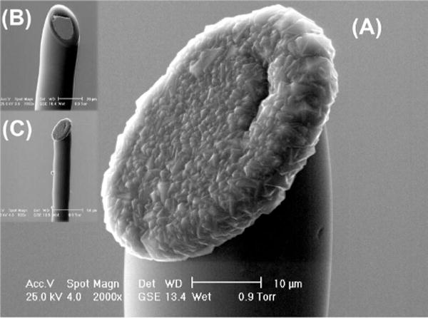
SEM images of (a) and (c) selective diamond deposition on a (b) tungsten microelectrode; final tip diameter is 35 μm. Negligible diamond growth is observed on the walls of the quartz insulating capillary.
III. INTEGRATED CIRCUIT ARCHITECTURE
Since physiological concentrations of various neurotransmitters are on the order of nanomolar, the neurochemical sensing circuitry typically needs to be able to measure currents on the order of picoamperes to nanoamperes, based on the transduction characteristics of a particular sensor. At the same time, current resolution levels of a few picoamperes might be required. Single-and multichannel integrated interface circuits for amperometric electrochemical biosensors [16]–[21] as well as for cell-based electrophysiological studies in patch-clamp applications [22] have been previously reported. In this paper, an integrated circuit for low-noise current measurements via an active wireless link has been developed that, compared to any previous reports, simultaneously achieves high current resolution and fast conversion speed in four wide-dynamic-range input current settings. This performance is primarily achieved by employing low-noise front-end design techniques on the transmitter side as well as efficient off-chip digital filtering on the receiver side.
Fig. 2 depicts the architecture of the proposed wireless neurochemical recording system, comprising an implantable integrated transmitter chip as well as external receiver electronics. On the transmitter side, the analog input current is directly converted to a serial data bit stream using an on-chip, first-order, current-input, ΔΣ modulator (ΔΣM). A low-power radio-frequency (RF) transmitter then sends the resulting digital data to the outside world at a carrier frequency near 433 MHz after Manchester encoding.
Fig. 2.
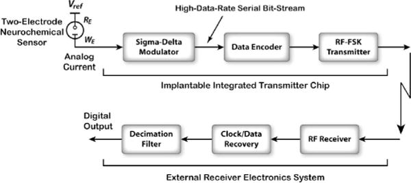
Schematic block diagram of the wireless neurochemical sensing system, comprising an integrated transmitter chip as well as external receiver electronics.
The direct conversion of the analog input current to a digital output bit stream alleviates the need for conventional current-to-voltage (I/V) converters based on operational amplifiers and resistors that can be inherently noisy and nonlinear, and thus unsuitable for low-current sensing applications.
On the receiver side, the encoded data are extracted using a commercially available, wideband, RF-to-IF2 down-converter followed by custom electronics for IF2-to-baseband conversion. The IF2 filter bandwidth is ±5 MHz centered around 10.7 MHz. Next, a Manchester decoder recovers the original clock and data signals, and a software-based decimation filter provides the final high-resolution digital output.
In this design, the decimation filter for the ΔΣM is implemented in software on the receiver side. Since the entire digital filtering stage is transferred from the on-chip implantable side to the external receiver side, significant reductions in silicon area and power consumption can be achieved. Moreover, the built-in flexibility of software implementation for the decimation filter allows one to dynamically tradeoff between the required resolution and data conversion speed.
A. Current-Input First-Order ΔΣ Modulator
Fig. 3 shows the schematic block diagram of the low-power, low-noise, first-order ΔΣM that lies at the core of the current-measuring circuitry. A two-stage operational amplifier featuring a simulated gain–bandwidth product of 1.9 MHz and a phase margin of 68° is used in the integrating stage. It consumes ~10 μA from a 2.6-V power supply. A 5-μW, clocked, binary comparator digitizes the analog output of the integrating stage with a sampling frequency of 130 kHz. The latching clock is delayed by 22.5° with respect to the comparator clock in order to allow the data to settle prior to latching. In this architecture, reference current sources are the main contributors to the input-referred noise. The current source transistors are laid out as wide-channel matched transistors in a 2-D common-centroid topology to reduce the input-referred offset current and noise that can directly corrupt very-low-current measurements.
Fig. 3.
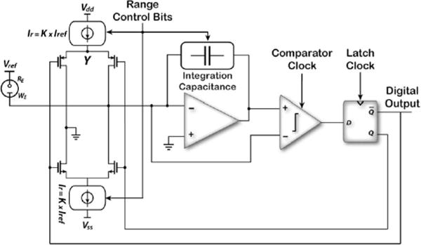
Schematic block diagram of the current-input, first-order, front-end ΔΣ modulator.
The ΔΣM is designed to operate in four different regions depending on the input current dynamic range. Region A corresponds to the maximum dynamic range of ±600 nA (i.e., ±Iref). Regions B, C, and D correspond to input current dynamic ranges of ±150, ±37.5, and ±4.7 nA, respectively. In order to maintain a constant sampling frequency, range changes can be accomplished by scaling the reference current Iref and the integrating capacitance using externally applied range control bits. The reference current can be scaled down by either: 1) switching in smaller current sources (e.g., a fraction of the original Iref) or 2) modulating the duty cycle of Iref in each sampling cycle to reduce its effective value [19], [20]. It should be noted, however, that method (1) cannot be employed arbitrarily, because the achievable offset and noise performances of very-low-amplitude matched current sources are largely process-dependent. As a result, a combination of the two techniques is employed as schematically depicted in Fig. 4 and tabulated in Table I.
Fig. 4.
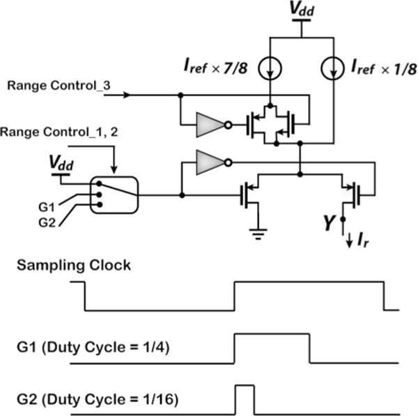
Illustration of range selection mechanisms. (Top) Circuitry for scaling Iref. (Bottom) G1 and G2 signals drawn with respect to the sampling clock for modulating the duty cycle of Iref in method (2). Sampling occurs at the negative edges.
TABLE I.
SUMMARY OF RANGE SELECTION MECHANISMS
| Region | K* | Iref × 1/8 Switched in | Iref × 7/8 Switched in | Duty Cycle Modulation (G1) | Duty Cycle Modulation (G2) | Integration Capacitance |
|---|---|---|---|---|---|---|
| A | 1 | √ | √ | – | – | 8pF |
| B | 1/4 | √ | √ | √ | – | 2pF |
| C | 1/16 | √ | √ | – | √ | 0.5pF |
| D | 1/128 | √ | – | – | √ | 80fF |
See Fig. 3.
The 600-nA reference current Iref is divided into two smaller current sources of 0.125 × Iref and 0.875 × Iref. For operation in Region A, both current sources are switched in and no modulation of the duty cycle is performed. For operation in Regions B and C, both current sources are switched in again and duty cycle modulations of 25% and 6.25% are applied, respectively. For operation in Region D, only the smaller current source (i.e., 0.125 × Iref) is switched in with a duty cycle modulation of 6.25%. The integration capacitance is divided into four parts as well and switched in according to the operation region, as also summarized in Table I. The ΔΣM occupies an active area of 420 μm × 210 μm in a 0.5-μm CMOS process and consumes 22 μA from a 2.6-V supply.
B. RF Transmitter
A cross-coupled voltage-controlled oscillator (VCO) circuit for analog frequency-modulated data transmission has been previously reported in [23]. In this paper, we use a similar design with a different tuning scheme for digital frequency-shift-keyed (FSK) transmission, as shown schematically in Fig. 5. The oscillator tank employs a surface-mount, high-Q, off-chip inductor for low-power operation at a frequency near 433 MHz. The tank switched capacitors are implemented using positive-channel MOS (PMOS) transistors with source/drain/bulk connected to each other. Flexibility in selecting a suitable ΔF for the FSK transmitter is achieved by dividing the capacitors into two sets of binary-weighted elements that can be externally controlled with 3 bits. The negative-channel MOS (NMOS) control switches are optimally sized to reduce their resistance and parasitic capacitance. Using this tuning scheme, ΔF can be varied in the range of 2–14 MHz in steps of 2 MHz. The transmitter bias current Ib is externally controllable in the range of 100–500 μA. The VCO occupies an active area of 175 μm × 65 μm in a 0.5-μm CMOS process.
Fig. 5.
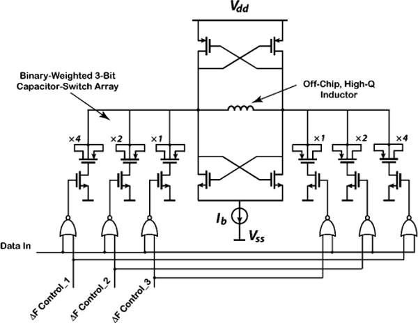
Transistor-level circuit schematic of the cross-coupled VCO for FSK transmission.
IV. MEASUREMENT RESULTS
A. Benchtop
A prototype integrated circuit was fabricated using the AMI 0.5 μm double-poly triple-metal n-well CMOS process, and measured 2.2 mm × 2.2 mm including the bonding pads. Fig. 6 shows a microphotograph of the fabricated chip. The chip was fully characterized for functionality during benchtop tests using a Keithley 6221 dc/ac current source [24].
Fig. 6.
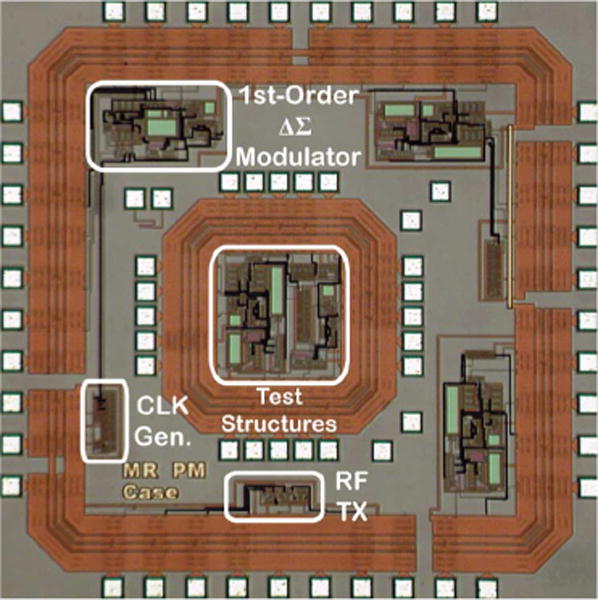
Microphotograph of the 2.2 mm × 2.2 mm chip fabricated using the AMI 0.5 μm 2P/3M n-well CMOS process.
Fig. 7 shows the wirelessly measured dc characteristics of the system with the input current varying in the range of 500 fA–600 nA in both positive and negative directions. The system achieved a highly linear response over six decades of the input current. DC current resolutions of ~17 pA, ~4.5 pA, ~1.5 pA, and ~250 fA were achieved in regions A, B, C, and D, respectively. In this test, the digital output of the system was decimated to 100 Hz at the receiver, and 100 samples were averaged per second to produce a dc current value. Current resolution in each operation region was reported as the measured peak noise on the resulting output current when the input current was lowered to a minimum value that could be measured with an error less than 50%. For example, in region D, the system was able to measure a minimum input current of 500 fA with a resolution of ±250 fA.
Fig. 7.
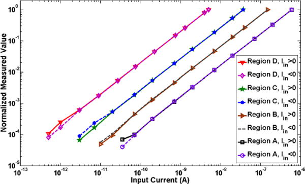
Wirelessly measured dc characteristics of the system with input current in the range of 500 fA–600 nA. Measured values in each region are normalized to the maximum value of the corresponding region (i.e., 600 nA, 150 nA, 37 nA, 5 nA for regions A, B, C, and D, respectively). High linearity is achieved over six decades of the input current.
Fig. 8 shows the system ac response for a 20-Hz, 100-pApp sinusoidal input current measured wirelessly at 430 MHz with the chip set to operate in region D (±5 nA). The decimation filter bandwidth was set to 50 Hz on the receiver side.
Fig. 8.
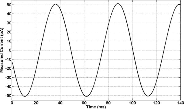
Wirelessly measured ac response of the system with a 20-Hz, 100-pApp sinusoidal input current. The recorded signal shown herein is input-referred. The chip is programmed to operate in region D (±5 nA).
B. Flow Injection Analysis
For neurotransmitter monitoring in flow injection analysis experiments, the fabricated CMOS chip was interfaced with a diamond-coated microprobe as the working electrode (WE). All measurements were collected in buffer containing 150 mM NaCl and 20 mM HEPES (pH = 7.4). The electrode was placed in a flow cell and buffer pumped at a rate of 2 mL/min. A bolus of dopamine at different concentrations was applied to the flowing stream via a loop injector driven by a pneumatic actuator.
A custom-written LabVIEW program was developed to apply the oxidation–reduction (redox) potential and initiate a chemical reaction. A chloridized silver wire (Ag/AgCl) was used as a standard electrochemical reference electrode (RE). The resulting current generated at the diamond electrode surface was then wirelessly reported by the chip. The redox potential was chosen where the oxidation current for dopamine was maximum, determined prior to this experiment by fast-scan cyclic voltammetry at the same diamond electrode. For all flow cell experiments, the chip was set to operate in region D (±5 nA).
Fig. 9 depicts the static calibration curve (current versus dopamine concentration) obtained in the flow cell for an applied potential of ~0.8 V versus Ag/AgCl where dopamine oxidation will occur. Dopamine concentration levels of 0.5, 2, 6.5, 10, 20, and 30 μM were applied. As can be seen, a highly linear response was achieved in a truly wireless measurement. Fig. 10 shows the dynamic plot (dopamine current versus time) with a dopamine concentration level of 20 μM injected into the flow cell.
Fig. 9.
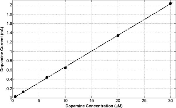
Wirelessly measured static calibration curve (current versus dopamine concentration). Dopamine concentration levels of 0.5, 2, 6.5, 10, 20, and 30 μM in an HEPES buffer are applied in the flow cell. The applied potential is ~0.8 V versus Ag/AgCl.
Fig. 10.
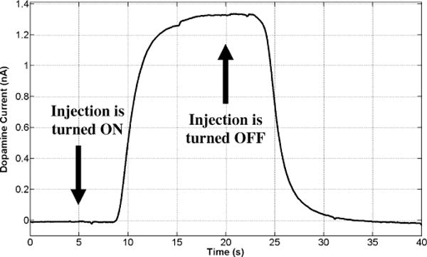
Wirelessly measured 20 μM dopamine current after 40 s of amperometry in flow injection analysis experiments. The current is measured in an HEPES buffer at the applied potential of ~0.8 V versus Ag/AgCl.
The rise and fall time instances within this temporal profile correspond to when dopamine injection was turned ON and OFF, respectively (i.e., 15 s bolus); these timestamps are offset from the actual increase and decrease of dopamine due to an inherent lag in the flow cell before electrolyte reaches the electrode.
Finally, Fig. 11 depicts the same plot with dopamine concentration level of 0.5 μM injected into the flow cell, resulting in a measured peak dopamine current of ~33 pA. Table II summarizes the measured performance of major circuitry and Table III compares the overall chip performance with that in recent published work.
Fig. 11.
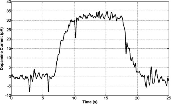
Wirelessly measured 0.5 μM dopamine current after 25 s of amperometry in flow injection analysis experiments. The current is measured in an HEPES buffer at the applied potential of ~0.8 V versus Ag/AgCl.
TABLE II.
SUMMARY OF MEASURED PERFORMANCE CHARACTERISTICS
| ΔΣ Modulator Sampling Rate | 130kHz |
| Decimated Sampling Rate | 100Hz |
|
Measured DC Current Resolution** Region A (±600nA) Region B (±150nA) Region C (±37nA) Region D (±5nA) |
~17pA ~4.5pA ~1.5pA ~250fA |
| Communication Scheme | FSK @ 433MHz |
| RF Data Transmission Rate | 260kb/s (Encoded) |
| Received Power at 0.5m | −60dBm (w/5-cm monopole TX and 50-cm RX antennae) |
| Power Supply | ±1.3V |
|
Power Consumption / Active Area Sensor Interface (ADC) RF Transmitter |
~57μW / 420μm × 2l0μm ~lmW / 175μm × 65μm |
| Technology | AMI 0.5μm 2P3M n-well CMOS |
See Section IV-A.
TABLE III.
RECORDING CHIP PERFORMANCE COMPARISON
| This Work | [18] | [19] | |
|---|---|---|---|
| Neurochemical Sensing Modality | Amperometry | Amperometry | Amperometry |
| # of Channels | 1 | 16 | 16 |
| Communication Scheme | FSK (Uplink) | Wired | Wired |
| Power Supply | ±1.3V | −2V; 7V | 3V |
| Current Resolution | ~250fA** in ±5nA ~1.5pA** in±37nA ~17pA** in ±600nA |
46pA in ±50nA lnAin±500nA (12-kHz BW) |
100fA in ±8pA (<0.1-HzBW) 15.3pAin±500nA (15-Hz BW) |
| Power Consumption (per channel) | 57μW | 780μW | 4.3μW (±8pA Range) 48.3μW (±500nA Range) |
| Technology | 0.5μmCMOS | 1.2μm BiCMOS | 0.5μmCMOS |
See Section IV-A.
V. CONCLUSION
In this paper, we reported on technology development at the sensor and circuit levels for wireless neurochemical monitoring using amperometry. Robust, versatile, implantable, microneedle electrodes were fabricated by chemical vapor deposition of highly conductive diamond onto the polished tip of a tungsten microelectrode. Moreover, integrated CMOS electronics were developed for conditioning and wirelessly transmitting the electrochemical signals corresponding to extracellular concentration variations of target neurotransmitters. Dopamine, a major electroactive neurotransmitter, with concentration levels as low as 0.5 μM was wirelessly recorded in flow cell by interfacing the diamond microelectrodes with the CMOS microelectronics.
Acknowledgments
The design, implementation, testing, and characterization of the integrated circuit were performed in the Electrical Engineering and Computer Science Department, Case Western Reserve University (CWRU), Cleveland, OH 44106 USA, and the diamond electrode development and flow injection analysis experiments were conducted in the Chemical Engineering Department at CWRU.
The work of P. Mohseni was supported by the Case Western Reserve University (CWRU) under Grant RES103289. The work of H. B. Martin was supported by the National Institute of Health (NIH)—-National Institute of Biomedical Imaging and Bioengineering (NIBIB) under Grant 1 R01 EB004018-01 A2.
Biographies

Masoud Roham (S’06) was born in 1979. He received the B.S. degree in electrical engineering from Amir-Kabir University of Technology, Tehran, Iran, in 2002, and the M.S. degree in electrical engineering from Sharif University of Technology, Tehran, Iran, in 2005. He is currently working toward the Ph.D. degree in the Electrical Engineering and Computer Science Department, Case Western Reserve University, Cleveland, OH.
His current research interests include analog/mixed-signal/RF integrated circuits and microsystems for neurotechnology with an emphasis on implantable devices for wireless monitoring of chemical signaling in the brain.

Jeffery M. Halpern was born in 1980. He received the B.S.E. degree in chemical engineering in 2003 from the Case Western Reserve University, Cleveland, OH, where he is currently working toward the Ph.D. degree at the Chemical Engineering Department.
His current research interests include novel diamond growth using chemical vapor deposition with an emphasis on electrochemical detection of neurotransmitters.

Heidi B. Martin received the two B.S. degrees in chemical engineering and chemistry and the Ph.D. degree in chemical engineering from the Case Western Reserve University, Cleveland, OH, in 1993 and 2000, respectively.
She was an NIH Postdoctoral Fellow, and worked in analytical chemistry at the University of North Carolina, Chapel Hill, NC. In 2002, she joined CWRU as an Assistant Professor of chemical engineering. Her current research interests include engineering of materials for biomedical and biochemical applications with emphasis on development of diamond electrodes for implantable electrochemical devices including neurosensors and neural/muscle stimulators.
Dr. Martin is a member of the Electrochemical Society, most recently as the Lead Organizer of the National Student Poster competition in the American Institute of Chemical Engineers. she cofounded the Sensors topical conference at the annual national meetings, serving as the Topical Chair for the last five years.

Hillel J. Chiel received the B.A. degree in English from Yale University, New Haven, CT, in 1974, and the Ph.D. degree in neural and endocrine regulation from Massachusetts Institute of Technology (MIT), Cambridge, in 1980.
He was a Postdoctoral Fellow at the Center for Neurobiology and Behavior, Columbia University’s College of Physicians and Surgeons and in the Department of Molecular Biophysics at AT&T Bell Laboratories. He joined the faculty of Case Western Reserve University, Cleveland, OH, where he is currently a Professor of Biology, with secondary appointments in the Departments of Neurosciences and Biomedical Engineering. His research has led to the development of novel technology for imaging muscle movements and neural activity in intact animals, and biologically inspired soft robots. He is a holder of two patents. He has published more than 85 peer-reviewed publications. His current research interests include biomechanical and neural mechanisms of adaptive behavior, using the marine mollusk Aplysia californica as a model system.

Pedram Mohseni (S’94–M’05) was born in 1974. He received the B.S. degree in electrical engineering from Sharif University of Technology, Tehran, Iran, in 1996, and the M.S. and Ph.D. degrees in electrical engineering from the University of Michigan, Ann Arbor, in 1999 and 2005, respectively.
He joined the faculty of Electrical Engineering and Computer Science Department, Case Western Reserve University, Cleveland, OH, as a tenure-track Assistant Professor in August 2005. He has authored or coauthored numerous papers in refereed IEEE journals and conferences, and has served as a Technical Reviewer for a number of the IEEE publications. His current research interests include analog/mixed-signal/RF integrated circuits and microsystems for neural engineering, wireless sensing/actuating systems for brain–machine interfaces, biomedical microtelemetry, and assembly/packaging of biomicrosystems.
Dr. Mohseni is an Organizer and Co-Chairman of the Advanced Neural Microsystems Special Session in the 2008 IEEE International Symposium on Circuits and Systems (ISCAS 2008), and a National Science Foundation (NSF) panelist in Biomedical Engineering. He is also a member of the Analog Signal Processing (ASP) and the Biomedical Circuits and Systems (BioCAS) Technical Committees of the IEEE Circuits and Systems society.
Footnotes
Color versions of one or more of the figures in this paper are available online at http://ieeexplore.ieee.org.
Contributor Information
Masoud Roham, Electrical Engineering and Computer Science Department, Case Western Reserve University, Cleveland, OH 44106 USA.
Jeffrey M. Halpern, Chemical Engineering Department, Case Western Reserve University, Cleveland, OH 44106 USA
Heidi B. Martin, Chemical Engineering Department, Case Western Reserve University, Cleveland, OH 44106 USA
Hillel J. Chiel, Biology Department, Case Western Reserve University, Cleveland, OH 44106 USA
Pedram Mohseni, Email: pedram.mohseni@case.edu, Electrical Engineering and Computer Science Department, Case Western Reserve University, Cleveland, OH 44106 USA, and also with the Advanced Platform Technology (APT) Center—A Veterans Affairs (VA) Research Center of Excellence, Cleveland, OH 44106 USA.
References
- 1.Zigmond MJ, Bloom FE, Landis SC, Roberts JL, Squire LR. Fundam Neurosci. San Diego, CA: Academic Press; 1999. [Google Scholar]
- 2.Kandel ER, Schwartz JH, Jessell TM. Principles of Neural Sci. New York: McGraw-Hill; 2000. [Google Scholar]
- 3.Glass M, Dragunov M. Neurochemical and morphological changes associated with human epilepsy. Brain Res Rev. 1995;21(1):29–41. doi: 10.1016/0165-0173(95)00005-n. [DOI] [PubMed] [Google Scholar]
- 4.Hasselmo ME, Hay J, Ilyn M, Gorchetchnikov A. Neuromodu-lation, theta rhythm, and rat spatial navigation. Neural Netw. 2002;15:689–707. doi: 10.1016/s0893-6080(02)00057-6. [DOI] [PubMed] [Google Scholar]
- 5.Lee K, Blaha C, Harris B, Cooper S, Hitti F, Leiter D, Roberts D, Kim U. Dopamine efflux in the rat striatum evoked by electrical stimulation of the subthalamic nucleus: Potential mechanism of action in Parkinson’s disease. Euro J Neurosci. 2006;23:1005–1014. doi: 10.1111/j.1460-9568.2006.04638.x. [DOI] [PubMed] [Google Scholar]
- 6.Wichmann T, Delong MR. Pathophysiology of Parkinsonian motor abnormalities. Adv Neurol. 1993;60:53–61. [PubMed] [Google Scholar]
- 7.Belayev A, Saul I, Liu Y, Ginsberg M, Valdes MA, Busto R, Be-layev L. Enriched environment delays the onset of hippocampal damage after global cerebral ischemia in rats. Brain Res. 2003;964:121–127. doi: 10.1016/s0006-8993(02)04089-1. [DOI] [PubMed] [Google Scholar]
- 8.Risedal A, Mattsson B, Dahlqvist P, Nordborg C, Olsson T, Johansson BB. Environmental influences on functional outcome after a cortical infarct in the rat. Brain Res Bull. 2002;58(3):315–321. doi: 10.1016/s0361-9230(02)00796-7. [DOI] [PubMed] [Google Scholar]
- 9.Hierlemann A. Integrated Chemical Microsensor Systems in CMOS Technology New York: Springer-Verlag. 2005. pp. 59–84. [Google Scholar]
- 10.Naware M, Thakor NV, Orth RN, Murari K, Passeraub PA. Design and microfabrication of a polymer-modified carbon sensor array for the measurement of neurotransmitter signals. Proc 25th Annu Int IEEE Eng Med Biol Conf (EMBC 2003); Cancun, Mexico. pp. 1952–1955. [Google Scholar]
- 11.Cahill PS, Walker QD, Finnegan JM, Mickelson GE, Wightman RM. Microelectrodes for the measurement of catecholamines in biological systems. Anal Chem. 1996;68:3180–3186. doi: 10.1021/ac960347d. [DOI] [PubMed] [Google Scholar]
- 12.Martin HB, Argoitia A, Angus JC, Landau U. Voltamme-try studies of single-crystal and polycrystalline diamond electrodes. J Electrochem Soc. 1999;146:2959–2964. [Google Scholar]
- 13.Suzuki A, Ivandini TA, Yoshimi K, Fujishima A, Oyama G, Nakazato T, Hattori N, Kitazawa S, Einaga Y. Fabrication, char-acterization, and application of boron-doped diamond microelectrodes for in vivo dopamine detection. Anal Chem. 2007;79:8608–8615. doi: 10.1021/ac071519h. [DOI] [PubMed] [Google Scholar]
- 14.Xie S, Shafer G, Wilson CG, Martin HB. In vitro adenosine detection with a diamond-based sensor. Diam Rel Mater. 2006;15:225–228. [Google Scholar]
- 15.Halpern JM, Xie S, Sutton GP, Higashikubo BT, Chestek CA, Chiel HJ, Martin HB. Diamond electrodes for neurodynamic studies in Aplysia californica. Diam Rel Mater. 2006;15:183–187. [Google Scholar]
- 16.Narula HS, Harris JG. VLSI potentiostat for amperometric measurements for electrolytic reactions,” in. Proc IEEE Int Symp Circuits Syst (ISCAS 2004); Vancouver, BC, Canada. pp. 457–460. [Google Scholar]
- 17.Zhang J, Trombly N, Mason A. A low-noise readout circuit for integrated electrochemical biosensor arrays. Proc IEEE Sens Conf; Vienna, Austria. Oct. 24–27, 2004; pp. 36–39. [Google Scholar]
- 18.Genov R, Stanacevic M, Naware M, Cauwenberghs G, Thakor NV. 16-channel integrated potentiostat for distributed neurochemical sensing. IEEE Trans Circuits Syst I, Reg Papers. 2006 Nov;53(11):2371–2376. [Google Scholar]
- 19.Stanacevic M, Murari K, Rege A, Cauwenberghs G, Thakor N. VLSI potentiostat array with oversampling gain modulation for wide-range neurotransmitter sensing. IEEE Trans Biomed Circuits Syst. 2007 Mar;1(1):63–72. doi: 10.1109/TBCAS.2007.893176. [DOI] [PubMed] [Google Scholar]
- 20.Murari K, Stanacevic M, Cauwenberghs G, Thakor NV. Integrated potentiostat for neurotransmitter sensing. IEEE Eng Med Biol Mag. 2005 Nov-Dec;24(6):23–29. doi: 10.1109/memb.2005.1549726. [DOI] [PubMed] [Google Scholar]
- 21.Gore A, Chakrabartty S, Pal S, Alocilja EC. A multichannel femtoampere-sensitivity potentiostat array for biosensing applications. IEEE Trans Circuits Syst I Reg Papers. 2006 Nov.53(11):2357–2363. [Google Scholar]
- 22.Laiwalla F, Klemic KG, Sigworth FJ, Culurciello E. An integrated patch-clamp amplifier in silicon-on-sapphire CMOS. IEEE Trans Circuits Syst I, Reg Papers. 2006 Nov.53(11):2364–2370. [Google Scholar]
- 23.Neihart NM, Harrison RR. Micropower circuits for bidirectional wireless telemetry in neural recording applications. IEEE Trans Biomed Eng. 2005 Nov.52(11):1950–1959. doi: 10.1109/TBME.2005.856247. [DOI] [PubMed] [Google Scholar]
- 24.Roham M, Mohseni P. Wireless amperometric neurochemical monitoring using an integrated FSK telemetry circuit,” in. Proc 3rd Int IEEE/EMBS Conf Neural Eng.; Kohala Coast. May 2–5, 2005; pp. 159–162. HI. [Google Scholar]


