

Abstract
Focused electron beam induced processing (FEBIP) is a suite of direct-write, high resolution techniques that enable fabrication and editing of nanostructured materials inside scanning electron microscopes and other focused electron beam (FEB) systems. Here we detail continuum techniques that are used to model FEBIP, and release software that can be used to simulate a wide range of processes reported in the FEBIP literature. These include: (i) etching and deposition performed using precursors that interact with a surface through physisorption and activated chemisorption, (ii) gas mixtures used to perform simultaneous focused electron beam induced etching and deposition (FEBIE and FEBID), and (iii) etch processes that proceed through multiple reaction pathways and generate a number of reaction products at the substrate surface. We also review and release software for Monte Carlo modeling of the precursor gas flux which is needed as an input parameter for continuum FEBIP models.
Keywords: continuum model, deposition, electron beam processing, etching, gas injection system
Review
Introduction to continuum models of focused electron beam induced processing (FEBIP)
Continuum FEBIP models enable the simulation of process rates that govern focused electron beam induced etching (FEBIE), deposition (FEBID) [1–16] and surface functionalization [17] techniques. They are typically used to simulate growth rates and nanostructure geometries as a function of experimental parameters, and to help elucidate the underlying growth mechanisms. Continuum FEBIP models are comprised of differential equations for the rates of change of concentrations of all surface-adsorbed species thought to be involved in the deposition or etch kinetics. The rate equations are functions of time and space, and require specification of the molecular properties of each adsorbate and the electron flux profile(s) at the solid–vacuum interface. Simple continuum FEBIP models can be solved analytically, yielding governing laws delineating the so-called “reaction-rate” and “mass transport” limited process regimes, and resolution scaling laws. Numerical models can account for adsorbate diffusion and enable modeling of processes such as simultaneous FEBIE and FEBID performed using a mixture of precursor gases. Here we provide software that can be used to simulate a wide range of processes reported in the FEBIP literature, and review the underlying continuum FEBIP models (recent general reviews of FEBIP can be found in [4,10,18–21]). We begin with a discussion of the reaction rate limited regime and the most common continuum model input parameters: initial adsorbate coverage, electron flux profile and the gas flux distribution produced by a capillary-style gas injection system. We then cover simple continuum models that are valid in the reaction rate limited regime (where net adsorbate transport via surface diffusion is negligible) and can be used to model FEBIP performed using continuous and pulsed electron beams, physisorbed and chemisorbed precursor molecules, gas mixtures, and multiple reaction products. Finally, we cover a number of models that account for surface diffusion and can be used to model FEBIP in both the reaction and mass transport limited regimes. Throughout, we emphasize the underlying assumptions and limitations inherent to each model.
Before beginning our discussion, we note that the terms “rate”, “concentration” and “flux” are always used to describe quantities with units of reciprocal time [s−1], reciprocal area [Å−2] and their product [Å−2s−1], respectively. For example, the concentration of adsorbate species ‘a’, Na, their desorption rate ka and desorption flux Naka have units of [adsorbates/Å2], [molecules/s] and [molecules/Å2/s], respectively. Frequently used symbols in this review are defined in Table 1. The term “growth” is applied to both FEBIE and FEBID (positive and negative growth rates refer to the growth of deposits and etch pits, respectively). We limit our discussion to FEBIP performed using a stationary, continuous or pulsed, radially symmetric electron beam (i.e., models implemented in cylindrical coordinates). Examples of models of scanned beams can be found in [22–24].
Table 1.
Guide to commonly used symbols.
| symbol | units | definition |
| Θ | Å−2 | adsorbate coverage |
| Λ | Å−2s−1 | adsorption flux |
| Ω | Å or nm | standard deviation of a Gaussian beam |
| δ | Å | molecule diameter |
| κ | s−1 | desorption attempt frequency |
| κD | Å−2s−1 | diffusion coefficient pre-factor |
| λ | m | mean free path |
| σ | Å2 | cross-section |
| τ | s−1 | residence time |
| A | Å2 | adsorbate area |
| D | Å2s−1 | diffusion coefficient |
| E | eV | energy |
| F or J | Å−2s−1 | gas molecular flux |
| N | Å−2 | adsorbate concentration |
| P | Pa or mbar | gas pressure |
| T | K | substrate temperature |
| Tg | K | gas temperature |
| V | Å3 or nm3 | volume |
| d | μm | GIS capillary diameter |
| f | Å−2s−1 | electron flux |
| h | Å or nm | height |
| k | s−1 | desorption rate |
| kB | eV·K−1 | Boltzmann’s constant |
| n0 | Å−2 | maximum (monolayer) adsorbate concentration |
| s | N/A | sticking probability |
Reaction rate limited growth regime
In order to reach clear conclusions it is often desirable to perform simulations and experiments under simplified conditions where one or more processes are negligible. In the case of FEBIP models, a useful simplification occurs when the net transport of adsorbates via surface diffusion is negligible. This condition can be met by performing FEBIP in the so-called reaction rate limited growth regime (also called the electron-limited growth regime) where the extent of adsorbate depletion caused by electrons is negligible [4,10,19–21]. The strict definition of reaction rate limited growth is that the electron-induced dissociation rate is much smaller than the sum of the adsorption rate and the thermal desorption rate, i.e., using the symbols defined below and in Table 1, for adsorbate species ‘a’,  . Conversely, the mass transport limited growth regime (also called the adsorbate-limited growth regime) is defined as
  . In the mass transport limited regime, the magnitude of the electron flux is sufficiently high to cause significant depletion of precursor adsorbates, and adsorbate diffusion into the area irradiated by electrons makes an important contribution to the growth rate.
In practice, the reaction rate limited regime can be identified simply by measuring or simulating the steady state growth rate as a function of electron flux, as illustrated in Figure 1 (in the figures, numerical values are excluded from axis labels when the plots are used to illustrate general trends that occur under a wide range of FEBIP conditions). Here, the linear portion of the curve corresponds to the reaction rate limited growth regime. In the mass transport limited growth regime, the deposit/pit shapes can provide information on the role of diffusion in the FEBIP process. Inclusion of diffusion in continuum FEBIP models adds a layer of complexity to the modelling and to interpretation of the model outputs. It is necessary only if diffusion is a major contribution to the growth rate. We will discuss models that incorporate diffusion in a self-contained section below, but will limit the majority of our discussion to diffusion-less models.
Figure 1.

Steady state vertical growth rate of a deposit plotted as a function of electron flux. The linear region of the curve in the limit of low electron flux corresponds to the reaction rate limited growth regime.
Initial adsorbate coverage
FEBIP models require specification of the initial concentration of surface-adsorbed precursor molecules  , i.e., the steady-state concentration of adsorbates in the absence of electron irradiation.
  can be found by solving for the difference between the flux of molecules adsorbing from and returning to the gas phase. In the gas phase, the molecule flux is given by:
 |
[1] |
where Pa is the pressure of the precursor gas for adsorbate ‘a’, ma is the mass of a gas molecule, kB is Boltzmann’s constant and Tg is the gas temperature. The simplest case of gas-molecule adsorption onto a substrate surface is that of physisorption, described by a single potential well at the surface as shown in Figure 2. The flux Λa of precursor molecules physisorbing to vacant surface sites is given by:
Figure 2.

Potential energy diagram for adsorption governed by a single potential well at the surface. Modified from [18].
| [2] |
where sa is the sticking coefficient (in the limit of zero surface coverage), and Θ is the adsorbate coverage, i.e., the fraction of surface sites occupied by physisorbed gas molecules:
| [3] |
where Aa is the area of a surface site occupied by adsorbate ‘a’, and 1/Aa is the maximum possible concentration of species ‘a’.
We note that Equation 2 describes non-activated Langmuir adsorption of a single molecular species ‘a’. The Langmuir model limits the surface coverage to one monolayer (hence the term (1 − Θ) in Equation 2), and can be modified to account for other adsorption behavior such as multilayer adsorption and thermally activated chemisorption. We also note that most FEBIP models assume that sa is independent of temperature.
The thermal desorption rate ka of the physisorbed species ‘a’ is given by:
| [4] |
where τa is the adsorption time (i.e., adsorbate residence time), κa is the desorption attempt frequency, Ea the desorption energy, (i.e., the depth of the potential well shown in Figure 2), and T is the temperature of the substrate surface. The thermal desorption flux is given by Naka, and the adsorbate concentration is found by solving
 |
[5] |
for Na(t):
 |
[6] |
In Equation 6, t = 0 represents the time at which the gas flux Fa is turned on in the model, i.e., the time at which the gas pressure is changed from 0 to Pa. A typical time-evolution of Na in the absence of electron irradiation is shown in Figure 3. As t → ∞, the surface coverage reaches a steady-state equilibrium value,  , which is the initial value that is input into FEBIP models (in which t = 0 represents the time at which the electron flux is turned on):
Figure 3.

Adsorbate concentration (Na) versus time in the absence of electron irradiation (here, Na = 0 at t = 0).  is the steady state adsorbate concentration in the absence of electron irradiation, which is used as the initial adsorbate concentration input into FEBIP models. Na(t) and
  are given by Equation 6 and Equation 7, respectively.
 |
[7] |
Electron flux profile
Spatially-resolved FEBIP models require specification of the electron flux profile f(r). Focused electron beams are usually approximated by a Gaussian function:
 |
[8] |
where Ω is the standard deviation (i.e., full width at half maximum, FWHM =  ) of the Gaussian beam. Defocused beams typically have a tophat shape that can be approximated by:
 |
[9] |
where f0 is the (maximum) flux at the beam axis (r = 0), β defines the abruptness of the edge of the tophat, and ξ is the beam radius. Tophat beams are useful for quantitative analyses and modeling of experimental data because they are easy to measure and control with a high degree of accuracy [2–3,6,25–26].
A Gaussian and two tophat electron flux profiles are shown in Figure 4. These profiles can be used to approximate those encountered in FEBIP. Actual flux profiles have contributions from primary, backscattered and secondary electrons, each of which has a unique spatial profile and a unique energy distribution [19].
Figure 4.

Gaussian electron flux profile (Ω = 10 nm) and two tophat flux profiles with a radius of 250 nm (β = 15 and 40). All three profiles are normalized to f0, the electron flux at the beam axis.
Gas flow from a capillary-style gas injection system (GIS)
FEBIP precursor gases are injected into a specimen chamber using one of two methods. In the first method, the entire vacuum chamber, or a sub-chamber [6] is filled with a precursor gas, as is done in environmental electron microscopy [27–30]. Such vacuum systems can be configured so that the gas pressure is uniform across the substrate surface, and can be measured accurately by conventional pressure gauges. However, in the vast majority of FEBIP setups, a gas injection capillary is used to inject the precursor gas into a chamber that is pumped continuously by a high-vacuum pumping system. The low conduction of the capillary makes it the element that limits the flow rate and shapes the flux profile of such gas injection systems. The capillaries are useful because they simultaneously assure a high local molecule flux at the substrate surface, and a low vacuum chamber background pressure, as required for robust operation of the vacuum system. However, a disadvantage of a capillary-style GIS is that the gas pressure varies dramatically throughout the chamber, and the gas pressure at the substrate surface cannot be measured accurately using conventional pressure gauges. Hence, in this section, we describe a Monte-Carlo simulator developed at Empa (the “GIS simulator”) for calculating gas pressure distributions generated by a capillary-style GIS. The code can be used to calculate the gas molecule flux at the beam impact point on the substrate surface (which is an input parameter to all FEBIP models).
Gas molecule impingement rates on the substrate have lateral distributions that depend on the capillary nozzle geometry, the angle and distance between capillary and substrate, and the molecule flow regime. The GIS simulator code enables the selection of some pre-defined nozzle geometries, capillary inner and outer diameters, angles and distances to the substrate, and either molecular or transient flow regime. By default it maps the impingement distribution on planar substrates, the molecule flux along the tube, and the angular nozzle effusion distribution. The code was validated by capillary injection experiments for both flow regimes [31–32].
Due to the Monte Carlo code implementation, the GIS simulator does not account for gas pressure gradients inside the capillary and above the substrate. The code can be used in an executable version or an editable version (http://www.empa.ch/febipcode) to include specific shadow effects by non-planar substrate geometries (such as deposits grown by FEBID), surface gas phase collisions, or other capillary geometries.
Flow regimes
To make a correct choice of the flow regime for the simulation one needs to determine the mean free path λ between molecule–molecule collisions and the Knudsen number (the ratio of λ to the capillary diameter d):
 |
[10] |
The Knudsen number specifies the ratio of wall collisions to molecule–molecule collisions. A value of 10 < Kn < ∞ signifies rare flow conditions under which the molecule gas flow distribution is determined predominantly by tube wall collisions (molecular flow regime). In the range 0.1 < Kn < 10 collisions between molecules become more important for shaping the flow (transient flow regime). When Kn < 0.1 the flow becomes viscous and can be treated by continuum models; this regime is not covered by the GIS simulator.
The calculation of the mean free path along a capillary is not trivial as the pressure P along the capillary is not constant. There will be a pressure gradient along capillaries directing net flow from the precursor reservoir (P≈ vapour pressure) to the vacuum chamber (P≤ 10−4 mbar) [33]. The commonly known relation  , where δ is the molecule diameter and other variables are as defined in Equation 1, can only be used if the pressure close to the capillary exit is known.
Mean free paths for a given GIS can be obtained by monitoring the precursor consumption rate Q (molecules per unit time) experimentally and calculating the mean free path using
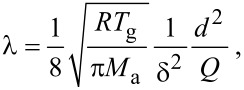 |
[11] |
where R is the ideal gas constant and M is the molar mass [33]. The Knudsen number can then be calculated by inserting Equation 11 into Equation 10. The consumption rate of the precursor can be monitored by measuring its mass or volume change due to evaporation during FEBIP. Alternatively, mass flow controllers can be used to supply a defined flow rate Q (sccm). Figure 5 shows the dependence of the Knudsen number on the pipe diameter for two flow rates of H2 and H2O. At a fixed flow rate and capillary diameter, the Knudsen numbers and mean free paths scale with  . Values for a few molecules are given in Table 2 together with their vapour pressure and monolayer adsorbate concentration n0 = 1/Aa = 1.154δ−2.
Figure 5.

Molecule flow regimes for two flow rates Q of H2 and H2O. Note that 1 sccm = 4.48 × 10¹⁷ molecules/second, using Avogadro’s number and the standard volume of 22.4 L/mol of an ideal gas at 0 °C and 1 atm.
Table 2.
Summary of molecule diameters (δ), molar masses (M), vapour pressures Pvap and monolayer adsorbate concentrations n0 of selected FEBIP precursors. The latter were calculated using n0 = 1.154δ−2.
| precursor | M [g/mol] | δ [Å] | n0 [nm−2] | Pvap [Pa/T] | Pvap ref. |
| Me3PtCpMe | 319.17 | 7.8a | 1.9 | 19/31 °C | [34] |
| TEOS:Si(OEt)4 | 208.33 | 8.1b | 1.8 | 172/25 °C | [36] |
| XeF2 | 169.29 | 4.5b | 5.7 | 598/25 °C | [37] |
| Me2Au(tfac) | 310.03 | 3.5a | 9.4 | 7.3/23 °C | [38] |
| W(CO)6 | 351.90 | 6.8b | 2.5 | 3.5/25 °C | [39] |
| Co2(CO)8 | 341.95 | 7a | 2.4 | 0.6...16/20 °Cc | [40] |
| Cu(hfac)2 | 477.65 | 8.0b | 1.8 | 0.4/25 °Cd | [41] |
| (hfac)Cu(VTMS) | 370.83 | 8.6b | 1.6 | 10/23 °C | [42] |
| [(PF3)2RhCl]2 | 628.48 | 5.7a | 3.6 | 7.5/23 °C | [38] |
| O2 | 16 | 3.7e | 8.4 | — | — |
| H2 | 2 | 2.7c | 15.8 | — | — |
| H2O | 18 | 3.5b | 9.4 | 2330/20 °C | [44] |
aLongest dimension of molecule.
bThe molecule size is determined from the compound density ρ according to δ = 1.122(M/(ρNA))1/3 where NA is Avogadro’s constant [35].
cCo2(CO)8 can disproportionate spontaneously in vacuum [40].
dCu(hfac)2 exists as dihydrate Cu(hfac)2·2H2O if not dried in vacuum with little effect on the vapour pressure [41].
eApparent diameters from [43].
To estimate an upper limit for the impingement rate, consider a substrate placed directly in front of a capillary with an exit area of 1 mm2 and a flow rate of 1 sccm. This results in a molecule flux Fa ≈ 4.5 × 10¹⁹ molecules cm−2s−1 leaving the capillary, or Fa ≈ 5 × 10⁵ monolayers per second (taking 1014 cm−2 as monolayer coverage). At a minimum, impingement rates of FEBIP molecules should be greater than the impingement rates of residual gases (at least one monolayer per second at a background pressure of 10−6 mbar). Of course, the molecule flux will rapidly decrease with distance between the capillary and the substrate.
Wall uptake
The GIS simulator incorporates an uptake factor for capillary wall collisions. Setting this value to zero means that all molecules colliding with the wall will immediately desorb; setting the value to 1 means that all molecules colliding with the wall will adsorb permanently (i.e., only molecules without wall collisions will exit the capillary). In most cases the uptake factor can be set to zero, as molecule condensation on capillary walls is normally avoided through the pressure gradient and keeping the reservoir at a temperature that is lower than or equal to that of the capillary walls. However, some organometallic molecules can spontaneously decompose in contact with the wall material and thus provide a surface for continuous autocatalytic decomposition through successive molecule–wall collisions. (Metal carbonyls are known for autocatalytic decomposition but data quantifying the uptake coefficients is sparse. A change in colour of the capillary points to such a mechanism). Analogous to the atomic layer deposition process [45], a more likely scenario is that at room temperature the molecules decompose partially via chemisorption upon collisions with unoccupied adsorption sites on the wall. This process is self-limiting after a short transient time during which all wall sites are occupied and the wall is passivated for further molecule decomposition.
Nozzle geometries
Two nozzle geometries are incorporated in the GIS simulator [31], and users can implement other geometries. Here we release the source code of version 1.5 containing the geometries shown in Figure 6 for straight capillaries and for bevelled capillaries with access holes. This C++ code is the base of the executable GIS simulator tool downloadable at http://www.empa.ch/febipcode. We would like to note that the code is not professionally commented nor written but has been checked against analytical solutions (for simple geometries) and against experiments. The current version of the code does not consider desorption of molecules from the substrate.
Figure 6.

Illustration of the two capillary nozzle geometries implemented in the GIS simulator. Left: straight capillary; right: bevelled capillary. Modified from [31].
Simulation method
The physics behind the GIS simulator is described in detail in [31,33,46] and we give only a brief summary here. The code is based on the so called test-particle Monte Carlo method, which works in the molecular and transient flow regimes. The molecule flux distribution is obtained as a function of the nozzle geometry and the arrangement of nozzle and substrate. Molecule trajectories are computed consecutively for 106 to 107 molecules. This approach is strictly only valid for molecular flow conditions where molecule trajectories are independent of each other, and collisions occur only with the inner tube wall. However, it was shown experimentally [31] and by comparison with direct simulation Monte Carlo [33] that the test-particle Monte Carlo method with intermolecular collisions gives excellent results in the following way (points 3 and 4 are simplifications, which can be changed by the user if required):
Transient flow simulations can be performed by setting the mean free path λ = d·Kn inside the entire capillary. The mean free paths should be calculated from precursor consumption measurements using Equation 11. The flow regime prevailing near the end of the capillary exit will then be entered correctly into the simulation.
Wall collisions are implemented such that the molecules leave the wall with a cosine distribution in space, while molecule–molecule collisions are implemented as a uniform angular distribution. The capillary entry distribution is implemented as a cosine point source. The implementation of these angular distributions of wall and molecule collisions was shown to be correct by independent experiments [31–32].
Outside of the nozzle the Knudsen number is set to infinity, i.e., molecules follow straight trajectories from the last collision inside the capillary until they hit the substrate (i.e., there are no molecule–molecule collisions outside the tube).
Consecutive trajectories inside the vacuum chamber are not taken into account (molecule desorption is neglected).
The capillary length must be entered into the simulation. For long capillaries this is an enormous computational effort. A reduced capillary length Lr can be entered instead, still giving accurate results. For molecular flow conditions, the spatial distribution of impinging molecules on the substrate is not significantly altered for lengths Lr > 15d. For transient flow conditions, the reduced length depends on λ with Lr = 3λ to 5λ [31,33].
Simulation examples with the GIS simulator
It is most useful to know how the nozzle geometry and the arrangement of the capillary with respect to the substrate influences the precursor flux at the substrate. The dependence of precursor flow on nozzle geometry (straight nozzle, bevelled nozzle with FEB access hole, closed capillary with FEB access holes), capillary angle, and shadowing by 3D objects have been studied by Friedli et al. [31,33]. More recently, it was shown that certain FEBIP scan strategies also lead to shadowing effects which can cause disruptions in surface flatness [23]. A specific simulation of a gas-flow distribution on a cantilever-based mass sensor enabled the estimation of the residence time of Me3PtCpMe on SiO2 [47]. With the released code the reader can include new nozzle geometries or substrate morphologies, for example a conical nozzle geometry as shown in Figure 7. With respect to the straight tube geometry the conical geometries are less practical for FEBIP in the molecular flow regime: Although cones “focus” the exiting molecules, they laterally reduce the maximum impinging flux area, physically cover the maximum flux area, and reduce the maximum impinging flux value slightly as shown by the J/Jtot contours. This behavior can be understood from the cosine-law redistribution of molecule collisions with the inner tube wall dominating the exiting precursor distribution in the molecular flow regime in contrast to the viscous flow experienced daily in water taps. Nonetheless, keeping the inner tube geometry straight and making the outer geometry conical could solve some space restrictions in the scanning electron microscope or allow to bring the nozzle closer to the substrate to increase the molecule impingement rate.
Figure 7.

Precursor flux distributions at the substrate under molecular flow conditions for conical nozzles with cone angles, θ, varying from 0° (straight tube) to 30°. The (0,0) position denotes the upper edge of the nozzle. Jtot is the total molecule flow leaving the nozzle exit and the color code indicates the molecule fraction J/Jtot. The cone geometries are shown to illustrate which areas are covered and hence inaccessible by the electron beam.
Single gas species FEBIP model: etching or deposition
In the following sections, we outline continuum FEBIP models that can be utilized to simulate a wide range of experiments reported in the FEBIP literature. We start with the simple case of a precursor gas comprised of a single molecular species “a” (i.e., an etch or deposition precursor) that physisorbs to the substrate surface. In this case, the continuum FEBIP model is based on an expression for the rate of change of the adsorbate concentration Na at each point r on the substrate surface. The expression for ∂Na/∂t is obtained by extending Equation 5 to account for the dissociation of adsorbates by electrons [16,19]:
 |
[12] |
This equation is a sum of fluxes representing gas molecule arrival at the surface through adsorption (Λa), adsorbate removal through thermal desorption (−Naka), and adsorbate conversion to fragment species through electron induced dissociation (−∂Nα/∂t). In Equation 12, t = 0 represents the time at which electron irradiation is activated in the model, and the initial adsorbate concentration  is given by Equation 7.
Most models of FEBIP assume that the adsorbate dissociation flux, ∂Nα/∂t, is proportional to the product of the electron flux f and Na:
 |
[13] |
where nα is the number of fragments α generated per dissociation event, and σα is the effective cross-section [3,18] for the generation of fragments that volatilize the substrate (in FEBIE) or deposit onto the substrate (in FEBID).
The steady state adsorbate concentration can be found by solving Equation 12 in the limit t→∞:
 |
[14] |
Substituting  into Equation 13 gives the steady state growth rate
  . The vertical growth rate ∂h/∂t, which is easily measured experimentally, is proportional to
  :
:
 |
[15] |
where h is the deposit height (or etch pit depth), ι is ±1 for deposition and etching, respectively, and VD is the volume of a single molecule removed from or added to the substrate in the etch or deposition reaction.
The electron flux f can either be fixed at f0, or specified by an r-dependent function such as Equation 8 or Equation 9. Setting f to f0 is justified when simulating the growth rate or the deposit height (etch pit depth) at the beam axis (r = 0). We emphasize that the above equations are valid only in the reaction rate limited growth regime where net transport of adsorbates through diffusion is negligible. We also note that electron-stimulated desorption (ESD) [48–51] is assumed to be negligible. This assumption is typically justified because, for most adsorbates, the ESD cross-section σE lies in the range from 10−7 to 10−2 Å2 [50] (i.e., in general, σE << σα). However, if necessary, ESD can be incorporated in the above FEBIP model simply by adding the term (−σEfNa) to Equation 12 [52].
Equation 15 can be used to calculate FEBIP growth rates as a function of experimental parameters such as the precursor gas pressure, electron flux and the substrate temperature. For example, Figure 8 shows a set of spatially resolved steady-state vertical growth rates calculated using a Gaussian electron flux profile and substrate temperatures of 300, 320, 340, 360 and 380 K. The growth rate decreases exponentially with temperature due to an increase in the thermal desorption rate ka (given by Equation 4).
Figure 8.

Steady state growth rate versus r calculated at a number of substrate temperatures using Equation 15 and a Gaussian electron flux profile (Equation 8, Ω = 5 nm).
Dimensionless FEBIP models
We now introduce a number of dimensionless parameters, originally employed by Utke et al. [15], which are useful for describing adsorbate kinetics in FEBIP [1] and giving concise scaling laws for the lateral resolution of the FEBIP process.
Irradiative depletion
 is a dimensionless parameter that quantifies the adsorbate concentration at the beam centre relative to the non-irradiated area. It is proportional to f0 and can be expressed as [53]:
| [16] |
The effective residence time in the absence of electron irradiation (or outside the irradiated area) τout,a is given by:
 |
[17] |
where τa is given by Equation 4, and n0 is the maximum possible adsorbate concentration (corresponding to one monolayer) in the absence of electron irradiation (i.e., n0 = 1/Aa).
The steady-state concentration of adsorbates under an electron beam, given by Equation 14, and the steady-state vertical growth rate defined by Equation 15 can now be reformulated as:
 |
[18] |
 |
[19] |
In the above,  is a dimensionless (normalized) version of the Gaussian or tophat electron electron flux profile given by Equation 8 or Equation 9, respectively, and
  is given by:
| [20] |
The lateral resolution can be quantified by the dimensionless parameter  , expressed as the ratio of the diameter of the deposit (FWHMD) and the electron beam (FWHM):
 |
[21] |
In the case of negligible surface diffusion,  can be derived analytically yielding the
  -vs-
-vs- scaling law of FEBIP resolution for stationary Gaussian [15] and tophat electron beams:
| [22] |
 |
[23] |
The resolution scaling behavior defined by the above equations is shown in Figure 9. In the limit of very low irradiative depletion  the resolution parameter is equal to 1, giving the highest possible FEBIP resolution (i.e., the smallest possible deposit size in the case of FEBID). In other words, the reaction limited (electron-limited) regime gives better lateral resolution than the mass transport limited (adsorbate-limited) regime. Deposits generated by tophat beams exhibit a less pronounced dependency of lateral resolution on irradiative depletion than those generated by Gaussian beams, and the dependence of
  on
on  is a function of the blurring parameter β (see Equation 9). However, tophat profiles typically have a much larger beam diameter 2ξ compared to the FWHM of a Gaussian.
Figure 9.

First FEBIP resolution scaling law for Gaussian and tophat electron beams.
Pulsed exposure: To illustrate the use of dimensionless parameters in FEBIP models, we consider the case of FEBIP performed using a pulsed, Gaussian electron beam. Specifically, we consider the adsorbate kinetics during an electron pulse, under the assumption that that the surface is replenished entirely between consecutive electron pulses. When the electron beam is turned on, the adsorbate concentration Na initially decays with time due to electron induced dissociation. The decay rate depends on the effective residence time τa,out and the irradiative depletion parameter  . The resulting time-evolution of Na is given by the solution to Equation 12, which can be expressed as:
 |
[24] |
The corresponding vertical growth rate is proportional to Na(t) and the electron flux, and is given by:
 |
[25] |
The lateral size of the growing structure or etch pit will evolve in time, yielding the  -vs-t law of pulsed FEBIP resolution, expressed as the lateral resolution
  , (neglecting surface diffusion) versus the electron beam exposure time t [1]:
 |
[26] |
In the limit t → 0,  . In the steady state (t → ∞) this converges to the scaling law given by Equation 22.
We note that Equation 8 and Equation 9 for the beam profile do not account for lateral contributions of backscattered and forward scattered electrons as well as their generated secondary electrons to the final shape of the deposit or etch pit. The above model also does not account for the change of those contributions on the developing three-dimensional pillar and etch-pit geometry. These simplifications limit the applicability of the resolution scaling laws given by Equation 22, Equation 23, and Equation 26 as well as Equation 27 and Equation 28 to aspect ratios of roughly 1 to 4 for deposits and etch pits. A more detailed discussion on the applicability range can be found in [10]. For high-aspect ratio structures either a full Monte Carlo electron trajectory approach can be chosen [54] or the continuum equations outlined in our present work need to be solved on a curvilinear reference surface, see [13] and [55].
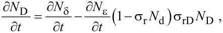
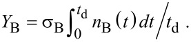
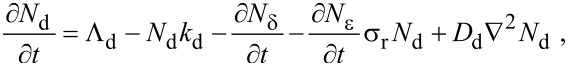
Multiple gas species FEBIP model: Simultaneous etching and deposition
Deposition and etching arising from electron-induced dissociation of multiple adsorbed species is important in a number of experimental processes. Deliberate use of a deposition and etch precursor gas mixture, as shown in Figure 10, is often advantageous, such as in the deposition of high purity materials using a FEBID precursor and an oxygen-containing background gas [56–63], or a mixture of two FEBID precursors [4,8,64–66]. Unintentional deposition of carbonaceous films through electron-activated cross linking of hydrocarbon contaminants is a common problem in many etch processes [6,9,14].
Figure 10.

Illustration of two adsorbate FEBIP where the molecules are supplied by two capillaries and impinge with fluxes Fe and Fd.
Simultaneous FEBID and FEBIE can be simulated using models such as those described in [11], with adjustment to account for system-specific details such as the surface site competition behavior of the etch and deposit precursor molecules, adsorbate–adsorbate interactions, and whether the etch precursor can volatilize all or only some fraction of the deposited material. A specific example of this is H2O-mediated FEBIE of deposits formed from organometallic precursors, where only the deposited carbon (and not the metal) is etched.
Here, we illustrate how simultaneous etching and deposition can be incorporated into a continuum FEBIP model for the case of a mixture of H2O and C10H22 as the precursors for etching and deposition of carbon, respectively [11]. In this model, we assume that both etch and deposition precursor adsorbates (denoted by the subscripts “e” and “d”, respectively) physisorb to the substrate surface (Figure 2) in a competitive process, with the total surface coverage Θ being limited to 1 ML. The fluxes and coverages of the two species are given by the following set of Equation 29–Equation 30:
 |
[29] |
 |
[31] |
| [32] |
| [33] |
| [30] |
Here, Equation 29 and Equation 31 are directly analogous to Equation 1, Equation 32 and Equation 33 are analogous to Equation 2, and Equation 30 is equivalent to Equation 3, modified to account for the fact that the adsorbates “e” and “d” physisorb to the surface and compete for the same surface sites. Growth rates can be found by solving differential equations for the rate of change of the concentration of the species “e”, “d” and “D”, where the latter denotes molecules that are deposited as a result of FEBID:
 |
[34] |
 |
[35] |
 |
[36] |
 |
[37] |
Equation 34 and Equation 35 are analogous to Equation 12, modified to account for the fact that FEBIE can volatilize the adsorbates “d” (i.e., the flux (∂Nε/∂t)σrNd represents FEBIE of the deposition precursor adsorbates). Equation 36 accounts for the simultaneous deposition of carbon through FEBID (∂Nδ/∂t) and volatilization of the deposit via EBIE [(∂Nε/∂t)(1 − σrNd)σrDND ], where (∂Nε/∂t)σrNd discounts those etch precursor fragments ε that are consumed in volatilizing the deposition precursor adsorbates “d”, and ND must be capped at 1/Ad so that only molecules in the top monolayer of the deposit are available for volatilization by the fragments ε. The reaction cross-section σr (and σrD) accounts for the effectiveness of collisions between the etch precursor fragments ε and the adsorbates “d” (or deposited molecules “D”) in contributing to etching [11]. Equation 37 is the vertical growth rate, and is directly analogous to Equation 15.
The fluxes ∂Nε/∂t and ∂Nδ/∂t represent electron-induced dissociation of the adsorbates “e” and “d”, respectively, and are given by:
 |
[38] |
 |
[39] |
where the symbols have the same meanings as in Equation 13. The thermal desorption rates ke and kd have the same functional form as Equation 4:
| [40] |
| [41] |
Initial concentrations of the species “e” and “d” (i.e., Ne0 and Nd0, respectively) can be found by solving Equation 34 and Equation 35 for the case of zero electron flux. The resulting time-evolution of surface coverage is more complex than that of the single gas species model shown in Figure 3, due to the nature of the surface site competition effect implemented in Equation 32–Equation 30. This is illustrated in Figure 11a for the case where Pe >> Pd and Ee << Ed. Initially, Ne increases much more rapidly than Nd because Pe >> Pd (and hence Fe >> Fd). However, at times greater than ca. 10−4 s the increase in Nd causes a corresponding decrease in Ne because the two species compete for the same surface sites and Ed >> Ee (and hence τd<< τe).
Figure 11.

(a) Adsorbate concentrations Ne and Nd versus time, calculated in the absence of electron irradiation (here, Ne = Nd = 0 at t = 0). Ne0 and Nd0 are the steady-state adsorbate concentrations in the absence of electron irradiation, which are used as the initial adsorbate concentrations input into FEBIP models defined by Equation 29–Equation 39. (b) Deposit geometries simulated using a Gaussian electron beam with a standard deviation (Ω) of 5 nm and a maximum flux (f0) of 1 × 10³, 2 × 10³ and 5 × 10³ Å−2s−1. (Etch species = H2O, deposition species = C10H22, Pe = 1 Torr, Pd = 0.01 Torr, se = 1, sd = 0.4, Ee = 0.56 eV, Ed = 1.0157 eV, κe = κd = 1016 s−1, σε = σδ = 1 Å2, σr = σrD = Ad = 74 Å2, T = Tg = 300 K. All other model input parameters were the same as in [11].)
The utility of the simultaneous FEBIE/FEBID model defined by Equation 34, Equation 35 and Equation 36 is illustrated in Figure 11b, which shows a number of deposits simulated using a Gaussian beam (given by Equation 8), with a maximum flux (f0) of 1 × 10³, 2 × 10³ and 5 × 10³ Å−2s−1. At the lowest electron flux (f0 = 1 × 10³ Å−2s−1), the deposit shape is approximately Gaussian because the extent of adsorbate depletion by the beam is low. At the intermediate flux (f0 = 2 × 10³ Å−2s−1), the central region of the deposit contains an indent caused by preferential depletion of the FEBID precursor adsorbates “d”. At the highest electron flux (f0 = 5 × 10³ Å−2s−1), FEBIE dominates in the central region of the deposit due to complete depletion of “d”. The preferential depletion of species “d” is a direct consequence of the slower replenishment rate caused by the fact that Pe >> Pd. The difference between the replenishment rates of “e” and “d” is illustrated in Figure 11a (at times shorter than ca. 10−5 s).
We emphasize that the changes in deposit geometry seen in Figure 11b are caused by a competition between simultaneous FEBIE and FEBID processes, and are not caused by adsorbate diffusion (which is ignored by Equation 29–Equation 39). This competition and the resulting phenomenon of electron flux controlled switching between etching and deposition have been discussed in detail in [11,14]. The additional effects of adsorbate diffusion can be investigated using a version of the above model that incorporates diffusion (discussed below).
Multiple adsorption states: Thermally activated chemisorption
The FEBID growth rate typically decreases with increasing substrate temperature (as illustrated by Figure 8) due to thermal depopulation of the physisorbed state shown in Figure 2. However, recently it was shown that activated chemisorption can give rise to a more complex dependence of the growth rate on T due to thermal population and depopulation of chemisorbed states [5,67]. The simplest case of a system that can undergo physisorption and activated chemisorption can be described by the potential energy diagram shown in Figure 12 [68], comprised of a physisorbed state (denoted “p”) and a chemisorbed state (denoted “c”) separated by an activation barrier for conversion between these states. The respective physisorption and chemisorption potential wells have depths Ep and Ec, and the activation barrier has height Econv.
Figure 12.

Potential energy diagram for the case of chemisorption governed by a potential well of depth Ec and an activation barrier of height Econv. Also shown is a physisorption potential well of depth Ep. Modified from [5].
Chemisorption is typically a dissociative process in which the activation barrier represents the energy needed to fragment the precursor molecule. For example, O2 chemisorbs onto numerous surfaces through the thermally activated reaction O2 → 2O, where O2 is in the gas phase or in the physisorbed state, and the two O atoms are in the chemisorbed state. Similarly, XeF2 can fluorinate many surfaces through decomposition pathways that generate chemisorbed F [17,69–71], and the FEBID precursor tetraethyl orthosilicate (TEOS, Si(OC2H5)4) chemisorbs onto SiO2 as a mixture of (SiO)2Si(OC2H5)2 and (SiO)Si(OC2H5)3 [72–74].
Chemisorption of gas phase precursor molecules can take place if their thermal energy is sufficiently high to surmount the barrier Econv − Ep (see Figure 12):
 |
[42] |
where sc is the sticking coefficient for activated sticking of gas molecules into the chemisorbed state (in the limit of zero surface coverage), s0 is the preexponential factor (i.e., the sticking coefficient for the limiting case of Econv − Ep = 0), and Tg is the temperature of the precursor gas. Similarly, molecules in the physisorbed state can surmount Econv by gaining thermal energy from the substrate and populate the chemisorbed state at a rate kconv:
| [43] |
This pathway is more relevant to FEBID than chemisorption from the gas phase (i.e., Equation 42) because FEBID is typically implemented as a cold-wall deposition technique, whereby Tg is dominated by the temperature of the capillary used to deliver the precursor gas, and the substrate temperature T is used to control growth kinetics.
The thermal desorption rates of physisorbed (kp) and chemisorbed species (kc) are given by:
 |
[44] |
| [45] |
Activated chemisorption can be incorporated into the continuum FEBID model by accounting for the above transitions between the gas phase, physisorbed and chemisorbed states by replacing Equation 12 with a pair of equations for the rate of change of concentration of physisorbed molecules (∂Np/∂t) and chemisorbed molecules (∂Nc/∂t) [5]:
 |
[46] |
 |
[47] |
and by replacing Equation 13 with:
 |
[48] |
where np and nc are the number of fragments generated per dissociation event of the physisorbed and chemisorbed molecules, respectively, assuming that both contribute to FEBID. Hence, the vertical growth rate is given by:
 |
[49] |
which assumes that the volumes of molecules deposited by the dissociation of physisorbed and chemisorbed adsorbates are both equal to VD.
The fluxes Λp, Λc and Λconv correspond to physisorption from the gas phase, chemisorption from the gas phase, and transitions from the physisorbed to chemisorbed states, respectively:
| [50] |
| [51] |
| [52] |
where Fa is the flux of precursor molecules “a”. The term (1 − sc) excludes gas molecules that are trapped in the physisorption potential well, and Θp and Θc are the coverages of physisorbed and chemisorbed adsorbates, each limited to 1 ML by:
| [53] |
| [54] |
We note that energetic electrons can cause partial decomposition of precursor molecules and hence induce transitions from the physisorbed to the chemisorbed state. This effect is neglected here, but can be incorporated into FEBIP models as in [17] for the case of fluorination caused by decomposition of XeF2.
The initial concentration of physisorbed  and chemisorbed
  species is found by solving Equation 46 and Equation 47 for the case of zero electron flux. An example of the pressure dependence of
  and
and  is shown in Figure 13a for a particular set of the energies Ep, Econv and Ec (corresponding to the chemisorption of TEOS onto SiO2 [5]), and substrate temperatures of 200, 300 and 350 K. The residence times of physisorbed and chemisorbed adsorbates are given by
  and
and  , which are governed by the depths of the chemisorption and physisorption potential wells shown in Figure 12. At a substrate temperature of 350 K, chemisorbed states are rapidly populated through the physisorbed state (Equation 43), but depopulate slowly as Econv
<< Ec (i.e., kconv
>> kc). Conversely, physisorbed states are rapidly depopulated because Ep is smaller than both Econv and Ec. Consequently,
, which are governed by the depths of the chemisorption and physisorption potential wells shown in Figure 12. At a substrate temperature of 350 K, chemisorbed states are rapidly populated through the physisorbed state (Equation 43), but depopulate slowly as Econv
<< Ec (i.e., kconv
>> kc). Conversely, physisorbed states are rapidly depopulated because Ep is smaller than both Econv and Ec. Consequently,  saturates at the monolayer limit of 1/Ac at a much lower pressure than
  saturates at the monolayer limit 1/Ap. At the lower substrate temperatures of 300 and 200 K, kconv, kp and kc are reduced through Equation 43, Equation 44 and Equation 45, yielding the adsorption isotherms shown in Figure 13a.
Figure 13.

(a) Steady state concentrations of physisorbed  and chemisorbed
  adsorbates versus pressure, calculated for the case of zero electron flux, and substrate temperatures of 200, 300 and 350 K. (b) Time-dependence of Np and Nc calculated for a substrate temperature of 300 K and a precursor gas pressure of 1 Torr. (In all cases, gas temperature = 300 K; Ep = 510 meV, Econv = 1.415 eV, Ec = 855 meV; f = 0; Ap = 2Ac and nc = 2 to represent a dissociative chemisorption process in which the precursor molecule fragments into two chemisorbed molecules. All other model input parameters were the same as in [5].)
It is important to note that the rate of chemisorption is always limited by the activation barrier shown in Figure 12. Hence, the rate at which physisorbed states are populated (and replenished during FEBID) is always greater than the rate at which chemisorbed states are populated. This is illustrated by the plots of Np(t) and Nc(t) shown in Figure 13b where, starting with a depopulated surface, the physisorbed species take ca. 10−6 s to populate the surface and reach a steady state, whereas it takes the chemisorbed species ca. 1 s to reach a steady state.
Equation 49 can be used to calculate the temperature-dependence of FEBID, as shown in Figure 14 for the case of TEOS [5]. The contribution to growth rate made by physisorbed adsorbates (i.e., fσpNp in Equation 48) decreases with increasing T due to an increase in the thermal desorption rate kp (and hence a decrease in the adsorbate coverage Np). The chemisorption component (i.e., fσcNc in Equation 48) is negligible at room temperature because Econv >> kBTg and Ec − Ep >> kBT. It is characterized by a peak produced by thermal conversion of adsorbates from the physisorbed to the chemisorbed state (i.e., the low-temperature tail of the peak) and desorption from the chemisorbed state (i.e., the high-temperature tail), respectively. The general temperature dependence seen in Figure 14 (i.e., a decrease in the physisorption component followed by a peak caused by chemisorption) exists only if kconv << kp << kc [5]. A practical benefit of performing FEBID at elevated temperatures (whereby, in this case, T ≥ 350 K) is that the deposits have much higher purity than those fabricated at room temperature [5].
Figure 14.

Steady-state vertical growth rate versus substrate temperature for a precursor that undergoes activated chemisorption described by the potential energy digram shown in Figure 12. The blue and red curves show contributions arising from electron induced dissociation of physisorbed and chemisorbed adsorbates, respectively. Modified from [5].
Role of multiple reaction products in electron beam induced etching
Etch processes such as XeF2-mediated FEBIE of SiO2 [12] and NF3 FEBIE of Si [2] proceed through multiple chemical pathways that involve a number of reaction products. Here, we use the case of NF3 FEBIE of Si [2] to illustrate how such processes can be incorporated in continuum FEBIE models.
FEBIE of Si using NF3 as the precursor gas involves the reaction products SiF, SiF2, SiF3, and SiF4, each of which can be dissociated by electrons, or can desorb from the substrate surface. For example, SiF2 can either gain F to form SiF3, dissociate to form SiF and F, or it can desorb (and hence give rise to etching by removing a Si atom):

Multi-step FEBIE reactions can be modeled using a set of differential rate equations that account for each molecular species at the substrate surface, which in this case are the NF3 precursor adsorbates (denoted by “a”), F radicals (α), and the reaction products SiF, SiF2, SiF3, and SiF4:
 |
[55] |
 |
[56] |
 |
[57] |
The symbols in Equation 55 and Equation 56 represent the same quantities as the corresponding symbols in Equation 12 and Equation 13 (see Table 1). In Equation 57, Nn (n = 1–4) represents the concentration of SiFn molecules, σr is the cross-section for the electron-induced scission of the Si–F bond, and kn is the desorption rate of SiFn:
| [58] |
where En is the binding energy of SiFn. Nη is the concentration of surface sites at which F can bond to a Si atom, and Θη is the coverage of surface sites occupied by F (see below in Figure 15):
Figure 15.

Flowchart showing how F radicals (represented by α) generated by electron induced dissociation of NF3 adsorbates (represented by the adsorbate concentration Na) are converted into SiFn (Nn) by reacting with SiFn−1 (Nn−1, shown in red). Horizontal green arrows indicate conversion of SiFn species by the addition and removal of F. The flowchart illustrates why m in Equation 59 ranges from 0 to 3 (corresponding to Nn−1, shown in red), and why n in Equation 60 ranges from 1 to 4 (corresponding to Nn, shown in black).
 |
[59] |
 |
[60] |
The term (1/n)ASi limits the concentration of fluorinated Si atoms to one monolayer, m is an integer with lower and upper limits of 0 and 3 because an unfluorinated Si atom (designated by m = 0) can react with F to form SiF, whereas SiF4 (designated by m = 4) cannot gain an additional fluorine atom. The integer n is bound by 1 and 4 because the total coverage of sites occupied by F must account for SiF, SiF2, SiF3 and SiF4 species. N0 (the concentration of unfluorinated Si atoms at the surface) is given by:
| [61] |
where ASi is the area of a single Si surface site, and NSi is the concentration of fluorinated Si sites:
 |
[62] |
The vertical etch rate is governed by the desorption rate of SiFn molecules:
 |
[63] |
Models such as the above (Equation 55–Equation 63) are typically based on a number of simplifying assumptions in addition to those made in simple FEBID models. This particular model assumes that all available F radicals generated by electron-induced dissociation of NF3 are converted to SiFn by reacting with SiFn−1, and that any surplus fluorine atoms desorb as shown in Figure 15 (the desorption is assumed instant, hence the absence of a desorption flux in Equation 56). The probability of a reaction between F and each species SiFn−1 is assumed equal and the total F coverage is limited to 1 ML, hence the term (Nn−1/Nη)(1 − Θη) in Equation 57 that governs the partitioning of the available F radicals illustrated by the flow chart shown in Figure 15. It is also assumed that σr is independent of n. Hence, the flux σrfNn+1 represents the creation of SiFn through electron-induced dissociation of SiFn+1, and −Nnσrf the consumption of SiFn through electron-induced dissociation of SiFn. Finally, it is assumed that electrons are not consumed in any of the reactions, and that electron-stimulated desorption of all species is negligible.
The most significant consequence of the model defined by Equation 55–Equation 63 is that etching is inhibited at high electron fluxes, as seen in Figure 16a, due to electron-induced dissociation of SiFn. Specifically, this effect dominates when the dissociation rate of species n is much greater greater than the corresponding thermal desorption rate (i.e., σrf >> kn). The simulations presented here were performed using model input parameters appropriate for cryogenic NF3-mediated FEBIP of Si performed at a substrate temperature of 100 K [2]. The model can be used to calculate a number of quantities such as the concentrations of NF3, SiF, SiF2, SiF3 and SiF4 molecules shown in Figure 16b, and the concentrations of unfluorinated (N0) and fluorinated (NSi) Si sites shown in Figure 16c.
Figure 16.

(a) Etch rate of Si calculated using Equation 63 as a function of electron flux f. (b,c) Corresponding steady state concentrations of NF3, SiF, SiF2, SiF3 and SiF4 molecules (Na and Nn), fluorinated (NSi) Si sites, and unfluorinated (N0) and Si sites. (T = 100 K, Tg = 300 K. All other model input parameters were the same as in [2].)
Special cases
The models outlined above can be used (either directly or in modified form) to simulate most processes reported in the FEBIP literature. Here, we summarize a few special cases for which the models require modification. We include these for completeness, and refer the reader to the cited papers for detailed descriptions of the changes that must be made to the above FEBIP models.
Adsorbate depletion in high aspect ratio pits [7]: The replenishment rate of precursor molecules consumed in FEBIE can be limited by the gas flow conductance of a growing etch pit. The replenishment rate affects the adsorbate concentration N which, in turn, affects the etch rate through equations such as Equation 15. Etch-pit conductance can be the most significant process limiting the FEBIE rate when fabricating high aspect ratio pits. As an etch pit grows during FEBIE, the conductance decreases, causing the etch rate to decrease with time as discussed in detail in [7].
Dynamic surface site activation during FEBIE [3]: Surface site activation caused by electron beam restructuring of the substrate (i.e., beam damage) can give rise to FEBIE of materials that can not be etched in their unmodified state. It can also alter etch kinetics, and cause the etch rate to increase with electron beam irradiation time.
Electron beam induced surface functionalization and spontaneous decomposition of precursor molecules at the substrate surface: These two processes have been modeled for the case of XeF2 [17] which can fragment through a dissociative chemisorption pathway, leading to fluorination of many surfaces [69–71,75]. The model in [17] is a variant of the above model of thermally activated chemisorption defined by Equation 42–Equation 54.
Electron beam dwell time as a control parameter of the composition of materials deposited using a mixture of two precursor gases [8]: This situation, depicted in Figure 10, can be modeled by solving rate equations for two FEBID precursor adsorbates, denoted by “A” and “B”, that compete for adsorption sites on the surface. The adsorbates are dissociated by electrons, producing non-volatile reactions products DA and DB (i.e., the deposit), and volatile reaction products VA and VB:

The evolution of the surface densities nA and nB of the two adsorbates is described by the following set of inhomogeneous first-order differential equations [8]:
 |
[64] |
 |
[65] |
The generic solution of this set as a function of electron-beam exposure (dwell time) is given by:
| [66] |
| [67] |
with the constants ndA,B, kd, ΔnA,B, κ defined in [8]. The dissociation yields YA,B are then obtained by integrating over the electron beam dwell time:
 |
[68] |
 |
[69] |
A graphical representation of Equation 68 and Equation 69 is shown in Figure 17. As the molecule fluxes, residence times, and dissociation cross-sections of molecules “A” and “B” are very likely different from each other, it can be seen that the composition (given by the magnitude Z on the right hand axis) of the deposits can be tuned by changing the electron beam dwell time per pixel. Equation 66 and Equation 67 hold for micrometer-sized deposits. For small-scale deposits surface diffusion can become important and different yields and compositions are obtained as function of exposure time, see Gabureac et al. [76–77]. Including surface diffusion into the multi-adsorbate model is straightforward, however, is at the expense of having a closed analytical solution.
Figure 17.

Calculated changes in dissociation yields YA and YB (per primary electron as defined in Equation 68 and Equation 69) and yield ratio Z versus electron beam dwell time. The example shown here was calculated for Co2(CO)8 and octanol as the deposition species “A” and “B”, respectively. The yield ratio Z is a measure for the ratio of non-volatile fragments of molecule “a” and “b” incorporated into the FEBID material. Taken from [78].
Diffusion
All of the above models are, strictly speaking, valid only in the reaction rate limited growth regime. They can be used to identify conditions under which depletion becomes significant, causing the system to transition into the mass transport limited regime (e.g., under intermediate and high electron flux conditions in Figure 11b, and the high electron flux portions of the curves in Figure 16). However, when the extent of depletion is significant (or, more precisely, when the net transport of adsorbates through diffusion is significant), the models must be modified to account for the diffusion of all mobile species at the surface. In the case of FEBID or FEBIE performed using a single species of physisorbed precursor molecules “a”, this is achieved simply by adding a diffusion term to Equation 12 [19]:
 |
[70] |
Da is the diffusion coefficient, given by:
 |
[71] |
where  is the energy barrier for diffusion and
  is the preexponential factor (i.e., the diffusivity in the limit
  ).
).
The above approach for incorporating diffusion can also be applied to more complex FEBIP models, as we illustrate below. We note, however, that all of the continuum models discussed here assume a flat substrate surface. That is, the models track the time-evolution of deposits and etch pits made by FEBIP, but do not account for the effects of the resulting changes in surface geometry on adsorbate kinetics (e.g., adsorption to and diffusion along the evolving pillar sidewalls or etch pit sidewalls).
Gas mixtures
Equation 34–Equation 37 are used to model a gas mixture comprised of an etch precursor “e” and a deposition precursor “d” that simultaneously etch and deposit a material such as carbon. To account for the diffusion of the adsorbates “e” and “d” at the substrate surface, Equation 34 and Equation 35 are replaced by [11]:
 |
[72] |
 |
[73] |
where De and Dd are the respective diffusion coefficients which have the same functional form as Equation 71:
 |
[74] |
 |
[75] |
Equation 36 and Equation 37 remain unchanged since localized FEBIP requires the substrate temperature to be sufficiently low for diffusion of the deposited species “D” (e.g., carbon) to be negligible.
Figure 18 shows deposit geometries simulated using Equation 72 and Equation 73, a Gaussian electron-beam profile and substrate temperatures of 285, 290 and 295 K. The dip in the center of each deposit is caused by the fact that etching dominates near the beam axis where the deposition precursor is preferentially depleted, while deposition dominates in the adjacent regions of low electron flux. The deposit geometry changes with temperature because an increase in T causes: (i) a decrease in Ne and Nd through thermal desorption (Equation 40 and Equation 41), and (ii) an increase in Ne and Nd through diffusion (Equation 74 and Equation 75). The dramatic change in geometry with increasing T shown in Figure 18 is largely due to reduced depletion of adsorbates “d” near the beam axis due to an increase in the rate of diffusion (Equation 75).
Figure 18.

Deposit geometries analogous to those shown in Figure 11b, simulated using Equation 72 and Equation 73, a Gaussian electron-beam profile (Ω = 5 nm) and substrate temperatures of 285, 290 and 295 K. (Etch species “e” = H2O, deposition species “d” = C10H22, f0 = 6 × 10⁴ Å−2s−1, Pe = 1 Torr, Pd = 0.01 Torr, Ee = 0.56 eV, Ed = 1.0157 eV, σβ = σγ = 1 Å2, Tg = 300 K. All other model input parameters were the same as in [11].)
Thermally activated chemisorption
The model of activated chemisorption described by the potential energy diagram shown in Figure 12 can be extended to account for diffusion by adding diffusion terms to Equation 46 and Equation 47:
 |
[76] |
 |
[77] |
 |
[78] |
 |
[79] |
where Dp and Dc are the diffusion coefficients for physisorbed and chemisorbed adsorbates, respectively.
Figure 19 shows FEBID rates simulated using Equation 76 and Equation 77, a Gaussian electron-beam profile and substrate temperatures of 300 K and 500 K. At 300 and 500 K, FEBID is dominated by electron-induced dissociation of physisorbed and chemisorbed gas molecules, respectively (see Figure 14), because of preferential population of the two respective states shown in Figure 12.
Figure 19.

FEBID growth rates simulated using Equation 77 and Equation 78, a Gaussian electron-beam profile (Ω = 5 nm) and substrate temperatures of (a) 300 K and (b) 500 K. (Deposition precursor = TEOS, f0 = 103 Å−2s−1, P = 0.1 Torr, Tg = 300 K,  = 0.17 eV,
  = 0.472 eV,
  =
=  = 1011 Å−2s−1 all other model input parameters were the same as in [5].)
Dimensionless FEBIP models
In this section, we incorporate surface diffusion into the dimensionless FEBIP model, introduced above through Equation 16–Equation 26.
The magnitude of adsorbate surface diffusion with respect to the FWHM size of the beam can be correlated by introducing the dimensionless surface diffusion replenishment parameter:
 |
[80] |
Substituting the irradiative depletion  from Equation 16 and the surface diffusion replenishment
  to the adsorbate rate equation, it becomes solely dependent on those two parameters and can be solved numerically [79]. Very small values of the surface diffusion replenishment parameter (e.g.,
  = 0.052) have a negligible effect on the lateral growth rate, as shown by row 1 of Figure 20 and Figure 21. However, large values (e.g.,
  = 0.52) can alter the deposit geometries significantly, particularly in the case of a tophat electron beam (see rows 2 and 3 of Figure 20 and Figure 21). If the contribution of surface diffusion is very high (
 >> 0.1), adsorbate replenishment through this process dominates the growth kinetics. For example, when
  = 100, the deposit height is increased by a factor of 10 relative to the situation where adsorbate replenishment occurs only through adsorption from the gas phase.
Figure 20.

Examples of deposit geometries simulated using exposure times (t) of 5 ms; 10 ms; 50 ms; 100 ms, a Gaussian beam profile, and selected values of the maximum electron flux f0 and surface diffusion coefficient Da (sa = 1, Fa = 104 nm−2s−1, n0 = 2 nm−2, τa = 100 μs, σa = 0.013 nm2, Va = 0.2 nm3 and FWHM = 100 nm).
Figure 21.

Examples of deposit geometries simulated using exposure times (t) of 5 ms; 10 ms; 50 ms; 100 ms, a tophat beam profile, and selected values of the maximum electron flux f0 and surface diffusion coefficient Da (sa = 1, Fa = 10 4 nm−2s−1, n0 = 2 nm−2, τa = 100μs, σa = 0.013 nm2, Va = 0.2 nm3 and FWHM = 100 nm).
The resolution parameter  for a stationary Gaussian beam can be obtained from the deposit shape, using a numerical solution of Equation 70, and the expression for the growth rate given by Equation 15. The numerical result is very well approximated by the
  -vs-
-vs- scaling law of FEBIP resolution formulated in [1]:
 |
[27] |
The above formula shows that even a relatively small surface diffusion contribution can lead to a decreasing in the deposit and etch pit size, and thus an improved lateral resolution. Once surface diffusion overcomes irradiative depletion, the deposit or etch pit diameter will approach that of the beam ( = 1), as discussed in [1].
Pulsed exposure: Equation 70 can be solved numerically, and the corresponding general scaling law of FEBIP resolution, including irradiative depletion, surface diffusion, and exposure dwell time, can be approximated by [1]:
 |
[28] |
The dependencies of deposit geometry on the electron beam exposure time t, irradiative depletion  and surface diffusion path
  are shown in Figure 20 and Figure 21 for Gaussian and tophat beams, respectively. At short exposure times, depletion is negligible and the deposit shapes reflect the electron flux profiles. At long exposure times, the deposit geometry is determined by the extent of adsorbate depletion, and the relative contributions to adsorbate replenishment through diffusion and adsorption from the gas phase [1].
Conclusion
In summary, we have reviewed continuum modeling techniques developed by the authors that can be used to simulate most processes reported in the FEBIP literature. Accompanying this article, we have released a software implementing most of these techniques at http://www.empa.ch/febipcode.
The software release consists of the following:
An executable binary and C++ code of the GIS simulator for simulation of impinging molecule flux from capillary nozzles on plane substrates, which can be modified to generate Figure 7.
A MATLAB notebook for single physisorbed gas species dimensionless FEBIP model that solve Equation 70 and Equation 49 for Gaussian electron beam (Equation 8). This was used to generate Figure 20.
A MATLAB notebook for single physisorbed gas species dimensionless FEBIP model that solve Equation 70 and Equation 49 for tophat electron beam (Equation 9). This was used to generate Figure 20.
Eight Mathematica notebooks, detailed below, that illustrate implementation of FEBIP models of varying complexity.
FEBIP models implemented in Mathematica notebooks:
1. Single physisorbed gas species initial coverage calculator, used to generate Figure 3.
2. Single physisorbed gas species FEBIP model based on Equation 12. This model was used to generate Figure 8.
3. Gas mixture FEBIP model based on Equation 34–Equation 41 and used to generate Figure 11a. For this simulation, initial coverages can be calculated by setting the electron flux to zero.
4. Gas mixture FEBIP model that incorporates diffusion, based on Equation 72–Equation 75 and used to generate Figure 18 and Figure 11b (in the latter, the diffusion coefficients were made negligible).
5. Thermally activated chemisorption initial coverage calculator used to generate Figure 13.
6. Thermally activated chemisorption, based on Equation 46–Equation 54 and used to generate Figure 14.
7. Thermally activated chemisorption with diffusion, based on Equation 76–Equation 79 and used to generate Figure 19.
8. EBIE with multiple reaction products, based on Equation 55–Equation 63 and used to generate Figure 16. Initial coverages can be calculated by setting the electron flux to zero.
Gaussian (Equation 8) or tophat (Equation 9) focused electron beams can be used by selecting the appropriate equations in each notebook.
Acknowledgments
Contributions made by M.T. and C.L. were funded in part by FEI Company and the Australian Research Council (Project Number DP140102721). A.S. and I.U. acknowledge support by the COST Action CM1301 (CELINA).
This article is part of the Thematic Series "Focused electron beam induced processing".
References
- 1.Szkudlarek A, Szmyt W, Kapusta C, Utke I. Appl Phys A. 2014;117:1715–1726. doi: 10.1007/s00339-014-8751-2. [DOI] [Google Scholar]
- 2.Martin A A, Toth M. ACS Appl Mater Interfaces. 2014;6:18457–18460. doi: 10.1021/am506163w. [DOI] [PubMed] [Google Scholar]
- 3.Martin A A, Phillips M R, Toth M. ACS Appl Mater Interfaces. 2013;5:8002–8007. doi: 10.1021/am402083n. [DOI] [PubMed] [Google Scholar]
- 4.Huth M, Porrati F, Schwalb C, Winhold M, Sachser R, Dukic M, Adams J, Fantner G. Beilstein J Nanotechnol. 2012;3:597–619. doi: 10.3762/bjnano.3.70. [DOI] [PMC free article] [PubMed] [Google Scholar]
- 5.Bishop J, Lobo C J, Martin A, Ford M, Phillips M R, Toth M. Phys Rev Lett. 2012;109:146103. doi: 10.1103/PhysRevLett.109.146103. [DOI] [PubMed] [Google Scholar]
- 6.Lobo C J, Martin A, Phillips M R, Toth M. Nanotechnology. 2012;23:375302. doi: 10.1088/0957-4484/23/37/375302. [DOI] [PubMed] [Google Scholar]
- 7.Randolph S, Toth M, Cullen J, Chandler C, Lobo C. Appl Phys Lett. 2011;99:213103. doi: 10.1063/1.3662928. [DOI] [Google Scholar]
- 8.Bernau L, Gabureac M, Erni R, Utke I. Angew Chem, Int Ed. 2010;49:8880–8884. doi: 10.1002/anie.201004220. [DOI] [PubMed] [Google Scholar]
- 9.Toth M, Lobo C J, Lysaght M J, Vladar A E, Postek M T. J Appl Phys. 2009;106:034306. doi: 10.1063/1.3187926. [DOI] [Google Scholar]
- 10.Utke I, Hoffmann P, Melngailis J. J Vac Sci Technol, B. 2008;26:1197–1276. doi: 10.1116/1.2955728. [DOI] [Google Scholar]
- 11.Lobo C J, Toth M, Wagner R, Thiel B L, Lysaght M. Nanotechnology. 2008;19:025303. doi: 10.1088/0957-4484/19/02/025303. [DOI] [PubMed] [Google Scholar]
- 12.Lassiter M G, Rack P D. Nanotechnology. 2008;19:455306. doi: 10.1088/0957-4484/19/45/455306. [DOI] [PubMed] [Google Scholar]
- 13.Rykaczewski K, White W B, Fedorov A G. J Appl Phys. 2007;101:054307. doi: 10.1063/1.2437065. [DOI] [Google Scholar]
- 14.Toth M, Lobo C J, Hartigan G, Knowles W R. J Appl Phys. 2007;101:054309. doi: 10.1063/1.2437667. [DOI] [Google Scholar]
- 15.Utke I, Friedli V, Purrucker M, Michler J. J Vac Sci Technol, B. 2007;25:2219. doi: 10.1116/1.2789441. [DOI] [Google Scholar]
- 16.Christy R W. J Appl Phys. 1960;31:1680–1683. doi: 10.1063/1.1735915. [DOI] [Google Scholar]
- 17.Randolph S J, Botman A, Toth M. Part Part Syst Charact. 2013;30:672–677. doi: 10.1002/ppsc.201300036. [DOI] [Google Scholar]
- 18.Toth M. Appl Phys A. 2014;117:1623–1629. doi: 10.1007/s00339-014-8596-8. [DOI] [Google Scholar]
- 19.Utke I, Moshkalev S, Russell P. Nanofabrication Using Focused Ion and Electron Beams. Oxford, United Kingdom: Oxford University Press; 2012. [Google Scholar]
- 20.van Dorp W F, Hagen C W. J Appl Phys. 2008;104:081301. doi: 10.1063/1.2977587. [DOI] [Google Scholar]
- 21.Randolph S J, Fowlkes J D, Rack P D. Crit Rev Solid State Mater Sci. 2006;31:55–89. doi: 10.1080/10408430600930438. [DOI] [Google Scholar]
- 22.Szkudlarek A, Gabureac M, Utke I. ECS Trans. 2013;50:495–498. doi: 10.1149/05012.0495ecst. [DOI] [Google Scholar]
- 23.Winkler R, Fowlkes J, Szkudlarek A, Utke I, Rack P D, Plank H. ACS Appl Mater Interfaces. 2014;6:2987–2995. doi: 10.1021/am405591d. [DOI] [PubMed] [Google Scholar]
- 24.Winkler R, Szkudlarek A, Fowlkes J D, Rack P D, Utke I, Plank H. ACS Appl Mater Interfaces. 2015;7:3289–3297. doi: 10.1021/am508052k. [DOI] [PubMed] [Google Scholar]
- 25.Li J T, Toth M, Dunn K A, Thiel B L. J Appl Phys. 2010;107:103540. doi: 10.1063/1.3428427. [DOI] [Google Scholar]
- 26.Li J, Toth M, Tileli V, Dunn K A, Lobo C J, Thiel B L. Appl Phys Lett. 2008;93:023130. doi: 10.1063/1.2959112. [DOI] [Google Scholar]
- 27.Parsons D F. Science. 1974;186:407. doi: 10.1126/science.186.4162.407. [DOI] [PubMed] [Google Scholar]
- 28.Danilatos G D. Adv Electron Electron Phys. 1988;71:109–250. [Google Scholar]
- 29.Toth M, Knowles W R, Thiel B L. Appl Phys Lett. 2006;88:023105. doi: 10.1063/1.2161571. [DOI] [Google Scholar]
- 30.Toth M, Uncovsky M, Knowles W R, Baker F S. Appl Phys Lett. 2007;91:053122. doi: 10.1063/1.2768031. [DOI] [Google Scholar]
- 31.Friedli V, Utke I. J Phys D: Appl Phys. 2009;42:125305. doi: 10.1088/0022-3727/42/12/125305. [DOI] [Google Scholar]
- 32.Wanzenboeck H D, Hochleitner G, Mika J, Shawrav M M, Gavagnin M, Bertagnolli E. Appl Phys A. 2014;117:1749–1756. doi: 10.1007/s00339-014-8755-y. [DOI] [Google Scholar]
- 33.Friedli V, Wanzenboeck H D, Utke I. Gas Injection Systems for FEB and FIB Processing: Theory and Experiment. In: Utke I, Moshkalev S, Russell P, editors. Nanofabrication using focused ion and electron beams: principles and applications. Oxford, United Kingdom: Oxford University Press; 2012. ((Nanomanufacturing series)). [Google Scholar]
- 34.Xue Z, Thridandam H, Kaesz H D, Hicks R F. Chem Mater. 1992;4:162–166. doi: 10.1021/cm00019a032. [DOI] [Google Scholar]
- 35.Dayton B B. Foundations of vacuum science and technology. New York, NY, U.S.A.: Wiley-VCH; 1998. [Google Scholar]
- 36.van der Vis M G M, Cordfunke E H P. Thermochim Acta. 1995;265:129–134. doi: 10.1016/0040-6031(95)02403-O. [DOI] [Google Scholar]
- 37.Schreiner F, McDonald G N, Chernick C L. J Phys Chem. 1968;72:1162–1166. doi: 10.1021/j100850a014. [DOI] [Google Scholar]
- 38.Ohta T, Cicoira F, Doppelt P, Beitone L, Hoffmann P. Chem Vap Deposition. 2001;7:33–37. doi: 10.1002/1521-3862(200101)7:1<33::AID-CVDE33>3.0.CO;2-Y. [DOI] [Google Scholar]
- 39.Lander, J.; Germer, L. Technical Publication 2259, Met.Technol. 1948, 14, 1–41.
- 40.Chandra D, Lau K, Chien W-M, Garner M. J Phys Chem Solids. 2005;66:241–245. doi: 10.1016/j.jpcs.2004.10.001. [DOI] [Google Scholar]
- 41.Widmer M. Deposition Pyrolytique Induite par Laser de Microstructures en Cuivre a Partir de Precurseurs Volatils. Lausanne, Switzerland: Ecole Polytechnique Federale de Lausanne; 1992. [Google Scholar]
- 42.Choi K-K, Rhee S-W. Thin Solid Films. 2002;409:147–152. doi: 10.1016/S0040-6090(02)00118-9. [DOI] [Google Scholar]
- 43.Berman A. Vacuum Engineering Calculations, Formulas, and Solved Exercises. Oxford, United Kingdom: Elsevier; 1992. [Google Scholar]
- 44.Wagner W, Pruss A. J Phys Chem Ref Data. 1993;22:783–787. doi: 10.1063/1.555926. [DOI] [Google Scholar]
- 45.Puurunen R L. Chem Vap Deposition. 2005;11:79–90. doi: 10.1002/cvde.200400021. [DOI] [Google Scholar]
- 46.Utke I, Friedli V, Amorosi S, Michler J, Hoffmann P. Microelectron Eng. 2006;83:1499–1502. doi: 10.1016/j.mee.2006.01.136. [DOI] [Google Scholar]
- 47.Friedli V, Santschi C, Michler J, Hoffmann P, Utke I. Appl Phys Lett. 2007;90:053106. doi: 10.1063/1.2435611. [DOI] [Google Scholar]
- 48.Madey T E, Yates J T., Jr J Vac Sci Technol (N Y, NY, U S) 1971;8:525–555. doi: 10.1116/1.1315200. [DOI] [Google Scholar]
- 49.Drinkwine M J, Lichtman D. Prog Surf Sci. 1977;8:123–142. doi: 10.1016/0079-6816(77)90002-8. [DOI] [Google Scholar]
- 50.Madey T E, Yates J T., Jr Surf Sci. 1977;63:203–231. doi: 10.1016/0039-6028(77)90339-9. [DOI] [Google Scholar]
- 51.Ramsier R D, Yates J T., Jr Surf Sci Rep. 1991;12:246–378. doi: 10.1016/0167-5729(91)90013-N. [DOI] [Google Scholar]
- 52.Cullen J, Bahm A, Lobo C J, Ford M J, Toth M. J Phys Chem C. 2015 doi: 10.1021/acs.jpcc.5b00918. [DOI] [Google Scholar]
- 53.Szkudlarek A, Gabureac M, Utke I. J Nanosci Nanotechnol. 2011;11:8074–8078. doi: 10.1166/jnn.2011.5066. [DOI] [PubMed] [Google Scholar]
- 54.Smith D A, Fowlkes J D, Rack P D. Small. 2008;4:1382–1389. doi: 10.1002/smll.200701133. [DOI] [PubMed] [Google Scholar]
- 55.Fowlkes J D, Rack P D. ACS Nano. 2010;4:1619–1629. doi: 10.1021/nn901363a. [DOI] [PubMed] [Google Scholar]
- 56.Perentes A, Hoffmann P. J Vac Sci Technol, B. 2007;25:2233–2238. doi: 10.1116/1.2798746. [DOI] [Google Scholar]
- 57.Perentes A, Hoffmann P. Chem Vap Deposition. 2007;13:176–184. doi: 10.1002/cvde.200606583. [DOI] [Google Scholar]
- 58.Shimojo M, Takeguchi M, Furuya K. Nanotechnology. 2006;17:3637–3640. doi: 10.1088/0957-4484/17/15/003. [DOI] [Google Scholar]
- 59.Mølhave K, Madsen D N, Dohn S, Bøggild P. Nanotechnology. 2004;15:1047–1053. doi: 10.1088/0957-4484/15/8/033. [DOI] [Google Scholar]
- 60.Wang S, Sun Y-M, Wang Q, White J M. J Vac Sci Technol, B. 2004;22:1803–1806. doi: 10.1116/1.1761266. [DOI] [Google Scholar]
- 61.Mølhave K, Madsen D N, Rasmussen A M, Carlsson A, Appel C C, Brorson M, Jacobsen C J H, Bøggild P. Nano Lett. 2003;3:1499–1503. doi: 10.1021/nl034528o. [DOI] [Google Scholar]
- 62.Folch A, Servat J, Esteve J, Tejada J, Seco M. J Vac Sci Technol, B. 1996;14:2609–2614. doi: 10.1116/1.588994. [DOI] [Google Scholar]
- 63.Folch A, Tejada J, Peters C H, Wrighton M S. Appl Phys Lett. 1995;66:2080–2082. doi: 10.1063/1.113909. [DOI] [Google Scholar]
- 64.Porrati F, Kämpken B, Terfort A, Huth M. J Appl Phys. 2013;113:053707. doi: 10.1063/1.4790320. [DOI] [Google Scholar]
- 65.Winhold M, Schwalb C H, Porrati F, Sachser R, Frangakis A S, Kämpken B, Terfort A, Auner N, Huth M. ACS Nano. 2011;5:9675–9681. doi: 10.1021/nn203134a. [DOI] [PubMed] [Google Scholar]
- 66.Che R C, Takeguchi M, Shimojo M, Zhang W, Furuya K. Appl Phys Lett. 2005;87:223109. doi: 10.1063/1.2136071. [DOI] [Google Scholar]
- 67.Bishop J, Toth M, Phillips M, Lobo C. Appl Phys Lett. 2012;101:211605. doi: 10.1063/1.4767521. [DOI] [Google Scholar]
- 68.Brass S G, Ehrlich G. Phys Rev Lett. 1986;57:2532–2535. doi: 10.1103/PhysRevLett.57.2532. [DOI] [PubMed] [Google Scholar]
- 69.Winters H F, Coburn J W. Appl Phys Lett. 1979;34:70–73. doi: 10.1063/1.90562. [DOI] [Google Scholar]
- 70.Tu Y-Y, Chuang T J, Winters H F. Phys Rev B. 1981;23:823–835. doi: 10.1103/PhysRevB.23.823. [DOI] [Google Scholar]
- 71.Loudiana M A, Schmid A, Dickinson J T, Ashley E J. Surf Sci. 1984;141:409–416. doi: 10.1016/0039-6028(84)90140-7. [DOI] [Google Scholar]
- 72.Tedder L L, Crowell J E, Logan M A. J Vac Sci Technol, A. 1991;9:1002–1006. doi: 10.1116/1.577566. [DOI] [Google Scholar]
- 73.Tedder L L, Lu G, Crowell J E. J Appl Phys. 1991;69:7037–7049. doi: 10.1063/1.348932. [DOI] [Google Scholar]
- 74.Crowell J E, Tedder L L, Cho H-C, Cascarano F M, Logan M A. J Electron Spectrosc Relat Phenom. 1990;54:1097–1104. doi: 10.1016/0368-2048(90)80299-P. [DOI] [Google Scholar]
- 75.Hills M M, Arnold G S. Appl Surf Sci. 1991;47:77–90. doi: 10.1016/0169-4332(91)90104-R. [DOI] [Google Scholar]
- 76.Gabureac M S, Bernau L, Utke I. J Nanosci Nanotechnol. 2011;11:7982–7987. doi: 10.1166/jnn.2011.5067. [DOI] [PubMed] [Google Scholar]
- 77.Gabureac M S, Bernau L, Boero G, Utke I. IEEE Trans Nanotechnol. 2013;12:668–673. doi: 10.1109/TNANO.2013.2266733. [DOI] [Google Scholar]
- 78.Bernau L. Sub-Micron Nano-Composite CoC Hall Sensors by Focused Electron-Beam Induced Deposition for Microbead Detection. Lausanne, Switzerland: Ecole Polytechnique Federale de Lausanne; 2011. [Google Scholar]
- 79.Szkudlarek A. Surface kinetics of Focused-electron-beam-induced-deposition. Kraków, Poland: AGH University of Science and Technology; 2014. [Google Scholar]