

Abstract
We investigate the shape and size effects of gold metallic nanoparticles on the enhancement of exciton-plasmon coupling and emission of semiconductor quantum dots induced via the simultaneous impact of metal-oxide and plasmonic effects. This enhancement occurs when metallic nanoparticle arrays are separated from the quantum dots by a layered thin film consisting of a high index dielectric material (silicon) and aluminum oxide. Our results show that adding the aluminum oxide layer can increase the degree of polarization of quantum dot emission induced by metallic nanorods by nearly two times, when these nanorods have large aspect ratios. We show when the aspect ratio of these nanorods is reduced to half, the aluminum oxide loses its impact, leading to no improvement in the degree of polarization. These results suggest that a silicon/aluminum oxide layer can significantly enhance exciton-plasmon coupling when quantum dots are in the vicinity of metallic nanoantennas with high aspect ratios.
I. INTRODUCTION
It is well known that metallic nanoparticles (MNPs) have vast tunability in their plasmonic absorption spectrum and electric field distribution that is dependent upon their sizes and shapes.1–4 When a quantum dot (QD) is in close proximity to a MNP or a rough metal surface, there can be coupling between the metal plasmons and the QD excitons.5–9 By changing the size and shape of the MNP in this system, the effective field seen by the QD will also change, resulting in different photoluminescence characteristics of the QD. Various shapes of MNPs, such as spheres,10–12 wires and rods,13,14 and bow-ties,15,16 have been tested in conjunction with emitters or QDs and it has been shown that the presence of the MNP alters fundamental properties of the emitter, such as absorption of the emitter and energy decay rates of the excitons to plasmon modes. In other words, the coupling processes between the excitons and plasmons, as well as other fundamental parameters, can be modified based on the MNP shape. The modification of the decay rate and photoluminescence is distance dependent17,18 as well as shape dependent. Furthermore, it has been shown that the size of MNPs can also affect the fluorescence rate of a single molecule emitter12 and plasmonic enhancement of the energy transfer between QDs.19
The emission of a QD can also be enhanced due to a nearby MNP, even when the exciting optical field does not excite the MNP plasmons directly. Under this condition, the emission enhancement can be due to exciton-plasmon coupling, making the emission of the QD in the MNP-QD system partially polarized.6,20,21 This type of coupling allows the QD's dipole to excite plasmons in the MNP and, in turn, the plasmon field enhances emission of the QD. Because of this coupling, the QD emission inherits the polarization of the MNP near field.
In a previous report, we showed that a silicon (Si) layer covered with an ultrathin layer of aluminum (Al) oxide, when fabricated between arrays of gold nanorods (NRs) and an ensemble of QDs, is extremely conducive to efficient QD emission in the system.22 The report demonstrated that the Si layer, by itself, could only lead to a relatively small increase (2–3 times) in QD emission via plasmonic effects when the NRs were present. The combination of the Si layer with the ultrathin Al oxide layer on top, however, led to more than 18 times enhancement of QD emission, well beyond the normal plasmonic enhancement seen in the case when only the Si layer was present. The emission from the NR-QD systems with Si/Al oxide also exhibited a stronger polarization dependency than systems with just Si, which suggested that the Si/Al oxide interface provided more efficient coupling between the QD excitons and the NR plasmons. In these cases, the Al oxide passivated the amorphous Si layer by reducing defect sites, and also prevented the QDs from losing electrons to the Si layer by electrostatic shielding via its large and negative fixed potential.23,24 These properties of Al oxide, combined with the high-index advantages of Si, seemed to be major factors in the significant enhancement of the QDs in NR-QD systems. Further studies on this topic are required to understand how one can use the unique properties of the Si/Al oxide interface to significantly enhance exciton-plasmon coupling in such systems. This understanding can be beneficial, in particular, for applications wherein the exciton-plasmon coupling is used for sensors, switches, and investigation of various quantum-coherent properties of MNP-QD systems.25–32
In this paper, we aim to discover the impact of the size and shape of MNPs on the enhancement of the exciton-plasmon coupling caused by plasmonic effects in a Si/Al oxide environment. We demonstrate that in such an environment, the greatest enhancement happens when the MNPs are NRs or nanoantennas with large aspect ratio and strong transverse modes with frequencies similar to that of the QD emission. The emission enhancement factor of these large aspect ratio NRs was found to reach about 20 times. More importantly, we show that for these NRs, there is a much stronger polarization dependency of QD emission (about two times) when the Si/Al oxide interface is present compared to case when just Si is used. This suggests that the enhancement of the degree of polarization induced by the unique Si/Al oxide interface is mostly via augmentation of the contribution of the exciton-plasmon interaction. Using time-resolved measurement, we showed this can be the result of elongation of the QD lifetime by the interface, despite the possibility of energy transfer from the QDs to the NRs. These results are imperative to the study of optimized exciton-plasmon coupling in hybrid MNP-QD systems, wherein the observations made in this paper allow fabrication of efficient systems that can be used to study fundamental quantum processes of these systems or their biological/sensing applications.27–34
II. SAMPLES AND METHODOLOGY
We began the study by fabricating gold (Au) MNPs that were shaped like NRs. The NRs were fabricated onto glass substrates using standard electron beam lithography methods. Each glass substrate sample contained four arrays of Au NRs, with each array consisting of the same size of the individual NRs. The four arrays allowed us to take average measurements of NRs that were prepared identically. After the fabrication of the NRs, a layer of 15 nm Si was deposited on top through use of a Denton sputter system. In some samples, we also sputtered a 1 nm layer of Al oxide on top of the Si layer to form the intermediate Si/Al oxide layer. In either case, the distance from QD to MNP is large enough that Főrster resonant energy transfer (FRET) is negligible. The fabricated samples are schematically shown in Fig. 1. We used CdSe/ZnS QDs from NN-Labs, LLC that were coated with octadecylamine ligands. The QDs had an emission peak at 650 nm, and were deposited on the samples via centrifuge.
FIG. 1.
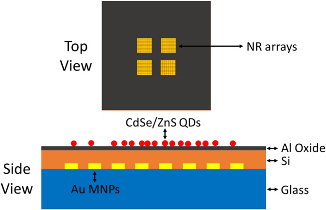
A top and side schematic of the fabricated sample device. Each device features four square regions of MNP arrays, shown in the top view. The side view shows the (not to scale) ordering of the glass substrate, Si, Al oxide, and QD layers. The NRs are embedded in the 15 nm Si layer. The side schematic shows Al oxide, but some devices we tested did not include Al oxide.
To excite the QDs on the samples, a continuous-wave 514 nm Ar ion laser was used in a spectroscopic setup. The laser light passed through an objective and irradiated the sample. Light from the sample returned through the objective and through a dichroic mirror. The dichroic mirror passed the light though a couple of filters and a lens to a fiber collimator. The light was collected by the collimator and sent to an Ocean Optics QE-Pro spectrometer. Polarization of the light emitted from the sample was analyzed by placing a variable linear polarizer in the setup after the dichroic mirror. The time resolved measurements were done using a Time Correlated Single Photon Counter (TCSPC) acquired from PicoQuant (TimeHarp 260).
The first NR size we investigated had average dimensions of 872 nm × 198 nm and had nominal thickness of 40 nm. The aspect ratio (longitudinal length divided by transverse width) was about 4.4. The arrays had row by column spacing between NRs of 0.5 μm × 1 μm, respectively. We give the label “type A” to these NR arrays. A SEM image of this type of NR array is shown in Fig. 2(a). Extinction spectra of these NRs were taken after the addition of Si/Al oxide to the top of the sample, by using a broadband white light source. The addition of the ultrathin Al oxide layer on top of the Si layer does not alter the absorption spectrum (this is true for all NR types used in this report). Comparison of the NR array absorption when the incident broadband light is longitudinally (along the longitudinal NR axis) and transversely (along the transverse NR axis) polarized is shown in Fig. 3(a). These absorption plots are the average of the four arrays. We noted that there was a drastic difference in the extinction spectra for the two perpendicular polarizations. Longitudinal incident light did not excite any strong plasmonic effects in type A NRs (line 1). With transverse polarization, however, the absorption of the NRs became featured, with a plasmonic peak at approximately 580 nm (line 2). Note that there is some coupling between the MNPs of the array, and their interaction with the incident light causes the sharp peak seen at 750 nm. This sharp peak can be due to diffraction scattering between the NRs.35,36
FIG. 2.

SEM images of the three types of NRs. Type A NRs are shown in (a), type B in (b), and type C in (c). A scale is shown at the bottom of each image.
FIG. 3.
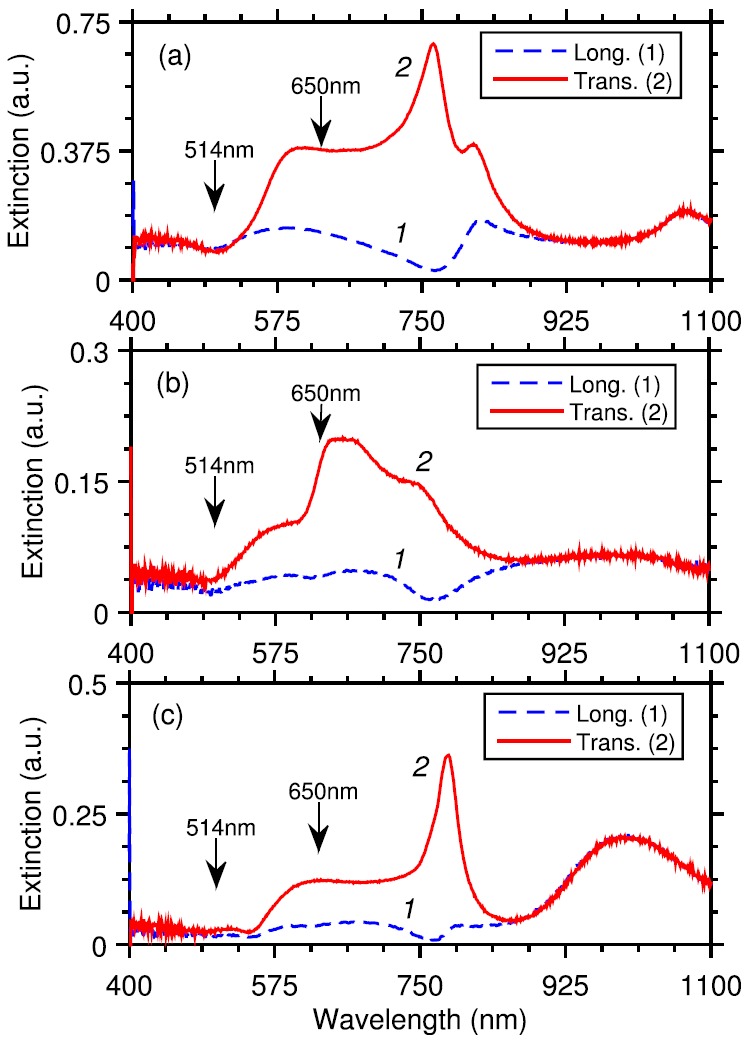
The absorbance spectrum of the three types of MNP arrays. In (a), we show type A; in (b), we show type B; and in (c), we illustrate type C. These absorbance measurements are taken after depositing Si and Al oxide. We denote transverse incident polarization by (1) and longitudinal polarization by (2).
The second type of NRs we studied was 393 nm × 133 nm in average size, and nominally 40 nm thick. The aspect ratio of these NRs was ∼3.0. The row by column spacing of the array was 0.5μm × 0.7 μm. We called NR arrays of this structure “type B.” A SEM image of this type of NR array is shown in Fig. 2(b), and the averaged absorption spectrum of the sample with a Si/Al oxide layer can be seen in Fig. 3(b). Here, again we observed that transverse polarized incident light excited a plasmonic peak in the NRs, whereas the longitudinal polarized light resulted in a flat absorption spectrum. The plasmonic peak when transverse incident light is used is approximately 650 nm.
The final type of NR we studied featured dimensions of 244 nm × 137 nm, was 40 nm thick, and had an aspect ratio of ∼2.0. The row by column spacing for this type was 0.5 μm × 0.5 μm. These were “type C” NR arrays. Fig. 2(c) shows a SEM image of this NR array. In Fig. 3(c), we compared the averaged extinction spectra of the NRs with a Si/Al oxide layer for the two polarizations. These NR arrays exhibited a very sharp peak when transverse incident light was used. This peak was centered at about 800 nm, and like in the case of type A NRs, we believe diffraction scattering could be responsible for this peak. In this paper, QD emission mostly falls on the plasmonic absorption of NRs, far from the collective resonances associated with such scattering.
III. RESULTS
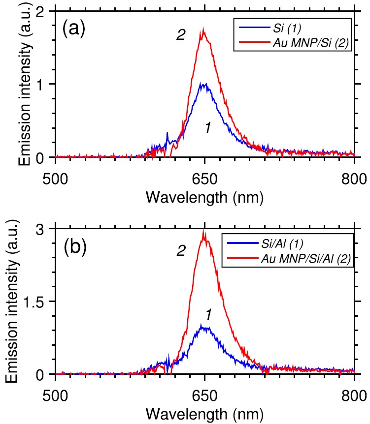
To understand how the size of the NRs in the arrays affects QD emission, we observed the QD emission on areas where NRs were present, and on areas where there were no NRs nearby. The results can be seen in Figs. 4–6, for which the data are the average of four measurements. In type A NR arrays, the samples with the Si layer exhibited enhanced QD emission when the NRs were present underneath the QDs. The enhancement factor due to the NRs (peak emission when NRs present divided by peak emission when NRs are absent) was 4.5 times. This is shown in Fig. 4(a). For the case where Si and Al oxide were deposited on top of these NRs, we observed an increased enhancement factor of 19.3 times (Fig. 4(b)). This was similar to the results reported in Ref. 22.
FIG. 4.
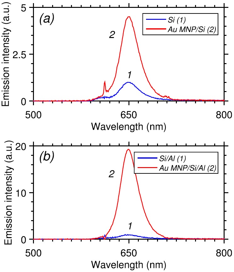
The QD emission from samples that contain type A NRs. In (a), we show the QD emission when a 15 nm layer of Si is present. Part (b) shows the QD emission when a 1 nm layer of Al oxide is coated on top of 15 nm Si.
FIG. 5.
The QD emission from samples that contain type B NRs. In (a), we show the QD emission when a 15 nm layer of Si is present. Part (b) shows the QD emission when a 1 nm layer of Al oxide is coated on top of 15 nm Si.
FIG. 6.
The QD emission from samples that contain type C NRs. In (a), we show the QD emission when a 15 nm layer of Si is present. Part (b) shows the QD emission when a 1 nm layer of Al oxide is coated on top of 15 nm Si.
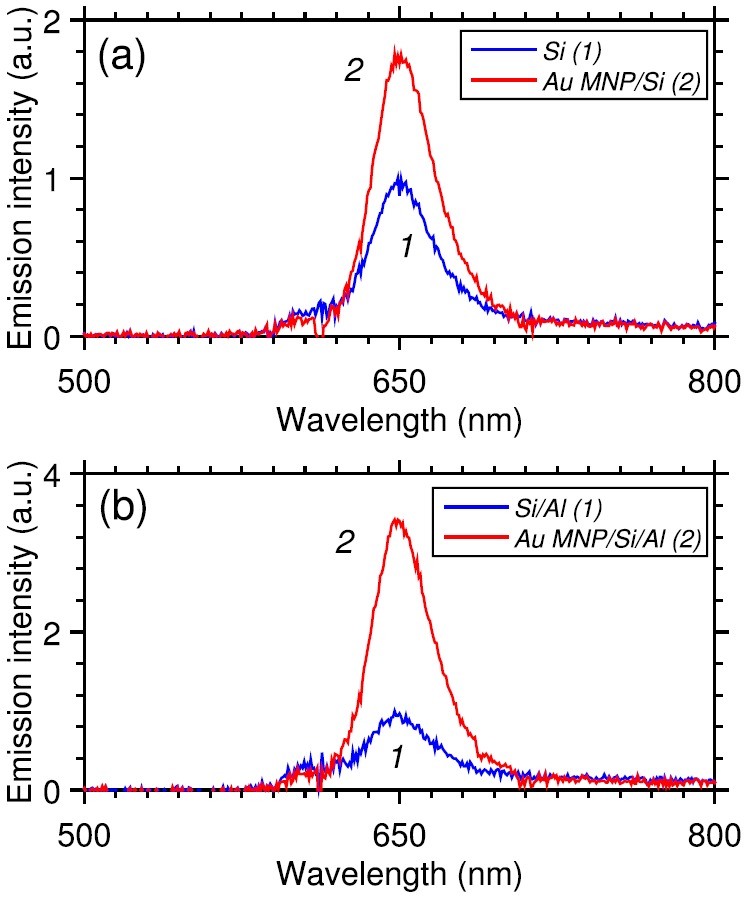
NR arrays of type B with a Si layer displayed an enhancement factor of 1.8 when the NRs were present. In Fig. 5(b), we see that replacing the Si layer with the Si/Al oxide intermediate layer led to an enhancement factor of 3.4 times.
Finally, we observed that type C NR arrays with an Si layer exhibited increased QD emission when NRs were present with an enhancement factor of about 1.7. In the Si/Al oxide intermediate layer case, we saw that the QD emission was enhanced by a factor of 2.9 when the NR arrays were present. These enhancement factors can be seen in Figs.6(a) and 6(b).
IV. ENHANCEMENT OF QD EMISSION POLARIZATION
The polarization dependency of all the samples was studied in order to determine the strength of exciton-dipole coupling in the systems (Fig. 7). In most cases, we saw that the peak emission occurred at an analyzer angle of 90°, which corresponded to QD emission along the transverse axis of the NRs. However, some of the samples had peak emission at other angles near 90°, such as 100 or 110°. This is because the sample may have been parallel tilted slightly with respect to the analyzer plane, or because the SEM processing occurred at a slight deviation angle from the sides of the sample. In Fig. 7(a), we observed that for type A NR arrays, the degree of polarization in QD emission increased from 23% to 41% when Al oxide was added on top of the Si layer. Type B NR arrays did not demonstrate any change in the degree of polarization with the introduction of Si/Al oxide, although there did exist some polarization dependency in both cases (Fig. 7(b)). In type C NRs, we see a very weak polarization dependency in samples with just Si, whereas the Si/Al oxide appeared to induce no polarization dependency at all (Fig. 7(c)).
FIG. 7.
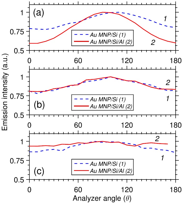
The emission dependence on analyzer angle. In (a), we show type A MNP polarization dependency, whereas (b) and (c) correspond to type B and type C polarization dependency, respectively. The dependence of samples with 15 nm and samples with 15 nm Si/1 nm Al oxide is shown for each type.
V. DISCUSSION
The results presented in the Section IV show that the QD emission enhancement caused by exciton-plasmon coupling can be controlled by adjusting the aspect ratio of the NRs that make up the array. This is true regardless whether the sample has a Si layer or a Si/Al oxide intermediate layer.6,20,21 The physical reason for this is because the amplitude and spectrum of the plasmonic peaks are changed for different aspect ratios (Fig. 3). We note that the laser excitation is at 514 nm, which occurs where there is negligible absorption of the NRs. This means that the enhancement of emission is not from the enhancement of the excitation source. Furthermore, there is also negligible difference in longitudinal and transverse absorption at this wavelength, meaning that the results we obtained are not impacted by the polarization of the laser. The amount of plasmonic absorption at the QD emission line is related to the strength of the exciton-plasmon coupling; more absorption means stronger plasmonic effects. We see that the relative transverse absorbance of type A, B, and C NRs is 0.375, 0.199, and 0.120, respectively. This suggests that type A NRs should have the most QD emission enhancement from exciton-plasmon coupling,36 and that type C NRs should exhibit the least. This is supported by the enhancement factors we found, for both Si and Si/Al oxide layers. Also note that the difference in absorption for transverse and longitudinal incident light polarization predicts the amount of polarization dependence in the QD emission. If is the difference in transverse and longitudinal absorption (αT − αL) at the QD emission line of 650 nm, then we see that type A NRs have of 0.25 compared to type B NRs, where the is 0.15. For type C NRs, the is 0.07. Not surprisingly, we see the most polarization-dependent QD emission in type A NRs. The main feature here, however, is the fact that the presence of Al oxide enhances this process significantly (Fig. 7(a)).
To discuss this further, note that the Si layer has high refractive index and, therefore, it can enhance the plasmonic effects and even collective modes of the NR arrays. This layer, however, can present a significant amount of defects, leading to fast non-radiative decay of excitons in QDs. The ultrathin Al oxide layer plays the major role of countering the disadvantages of Si as well as introducing an electrostatic shielding benefit of its own. This type of behavior has been described recently in Ref. 23. The Al oxide passivates the Si surface defects, so that fewer electrons can become trapped in them. Furthermore, the large negative potential introduced by Al oxide electrically repels the QD electrons from entering the Si layer defect sites, suppressing Auger processes. In this way, we have effectively reduced the disadvantageous Si layer properties. When comparing the QD emission of Si to Si/Al oxide cases in Fig. 7(a), we see that the degree of polarization is much greater when Al oxide is present than when it does not (by nearly two times). Since the difference in the NR extinction spectra between Si and Si/Al oxide is very small, this result gives a foundation to the argument that Al oxide, through its passivating and electrical properties, disfranchises the Si disadvantages and thereby strengthens the exciton-plasmon coupling via elongation of the QDs' radiative lifetimes. In Figs. 7(b) and 7(c), we see that the addition of Al oxide does not affect the polarization dependency of type B and C NRs as much as for type A NRs. This could mean that the exciton-plasmon coupling was not very strong in the first place, and placing an Si/Al oxide layer between the weakly coupled QD-MNP systems will not greatly increase the strength of coupling between them.
As highlighted in Fig. 8, even when θ = 0, i.e., the QD polarization is along the long axis of the NRs, the emission can undergo significant amount of enhancement, depending on the aspect ratios of the NRs ((a)–(c)). The emission enhancement factors, defined as the ratio of QD emission on glass to that on NRs, are shown Figs. 8(a′)–8(c′) for these NRs. For the largest aspect ratio (∼4.4), we observe emission enhancement of about 12 (Fig. 8(a′)). This value increases at θ = 90° when exciton-plasmon coupling associated with transverse modes of NRs maximizes. The enhancement at θ = 0 reduces to ∼2.7 and 2.5 as the aspect ratio decreases to ∼3 and ∼2, as can be seen in Figs. 8(b′) and 8(c′)). The significant enhancement in the case of the type A structure (aspect ratio ∼4.4), could be due to excitation of the longitudinal multipolar modes of the structure as it represents a metallic nanoantenna array that can support a plasmonic lattice.35,36
FIG. 8.
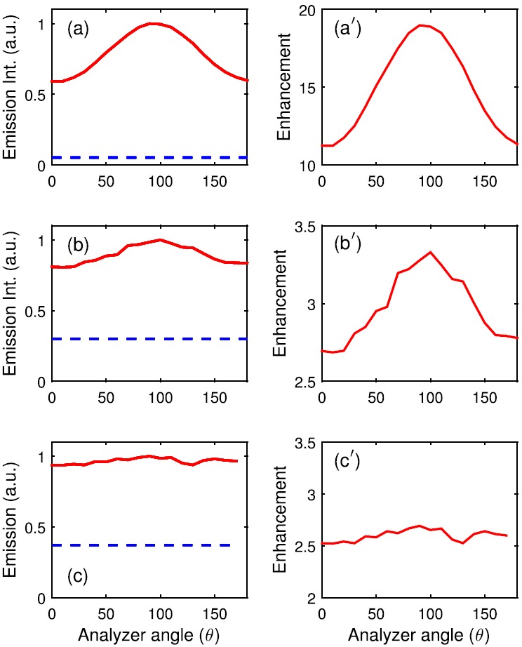
(a)–(c) emission intensity of QDs on the Si/Al oxide layer when Au NRs are absent (dashed lines) and present (solid lines). The horizontal axis represents the angle of the polarization analyzer placed before the spectrometer. In (a), we show the QD emission intensity for sample A NRs; in (b), we show sample B NRs; and in (c), we show sample C NRs. (a′), (b′), and (c′) represent the enhancement factors in these cases, respectively.
To explore the impact of Al oxide further, we carried out QD lifetime measurements using the TCSPC system. Fig. 9(a) shows the emission decay of the QDs in the absence of the NRs. The results show that the Al oxide layer can reduce the lifetime of the QDs. This is clearly highlighted via the bi-exponential fits to these decays (solid lines). These results suggest that for the type of QDs studied in this paper, Al oxide actually suppresses the emission of such QDs. This is consistent with our previous investigations that showed the impact of Al oxide is very dependent on the type of the substrate and the QDs.23,24 For types of QDs that exhibit active photo-chemical and photo-physical properties, Al oxide can lead to a significant amount of enhancement of emission efficiency of the QDs. We believe the reason behind the results seen in Fig. 9(a) is that the type of QDs used in this paper did not show any significant active photo-chemical or physical processes. This can partially be related to the fact that these QDs had a ZnS shell.
FIG. 9.
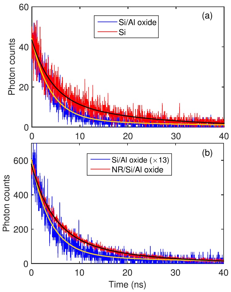
Time-resolved emission of QDs on Si and Si/Al oxide interfaces (a) and on Si/Al oxide in the absence of presence of NRs (b). Note in (b), the emission of the QD on Si/Al oxide in the absence of NR is multiplied by 13. The solids lines refer to bi-exponential fittings.
In Fig. 9(b), we compare the decay of QD emission on Si/Al oxide in the absence and presence of the NRs shown in Fig. 2(a). The results show that the presence of NRs increases the lifetime of the QDs, leading to very large enhancement of their emission (Fig. 4). This is a rather interesting result, since in the presence of the NRs, one expects the FRET from QDs to the NRs to reduce the lifetime of the QDs. Even for the optimized thickness of the Si layer (15 nm), which allowed the favorable impact of plasmon field enhancement to overcome the suppression caused by FRET, we expected some degree of reduction in lifetime. Instead, in Fig. 9(a), we see an enhancement of QD emission along with a longer QD lifetime even in the presence of FRET. This suggests that for the type of QDs used in this paper, the combined effects of Si and Al oxide layers and the Au NRs may be responsible for significant improvement of the radiative efficiency of the QDs via suppression of their non-radiative decay channels. Since in our systems plasmons were excited by the QD emission, this in turn enhances the exciton-plasmon coupling efficiency.
VI. CONCLUSIONS
We studied how the size and shape of Au NR arrays affect the QD emission in the presence of Si and Si/Al oxide intermediate layers. Reduction in the aspect ratio of the NRs was observed to reduce the impact of Al oxide on exciton-plasmon coupling and thus the QD emission enhancement seen when NRs were present. The largest enhancement and increase in degree of emission polarization caused by Si/Al oxide was seen in Au nanoantennas with large aspect ratio. This suggests that addition of Al oxide to form Si/Al oxide layer can drastically increase the degree of exciton-plasmon coupling.
ACKNOWLEDGMENTS
This work is supported by U.S. National Science Foundation under Grant No. CMMI 1234823. C.B.M. would like to thank the financial support from National Institutes of Health (EB015190) and National Science Foundation (DMR-0847758).
References
- 1. Kelly K. L., Coronado E., Zhao L. L., and Schatz G. C., J. Phys. Chem. B 107, 668 (2003). 10.1021/jp026731y [DOI] [Google Scholar]
- 2. Jain P. K., Lee K. S., El-Sayed I. H., and El-Sayed M. A., J. Phys. Chem. B 110, 7238 (2006). 10.1021/jp057170o [DOI] [PubMed] [Google Scholar]
- 3. Link S. and El-Sayed M. A., J. Phys. Chem. B 103, 4212 (1999). 10.1021/jp984796o [DOI] [Google Scholar]
- 4. Jensen T. R., Malinsky M. D., Haynes C. L., and Van Duyne R. P., J. Phys. Chem. B 104, 10549 (2000). 10.1021/jp002435e [DOI] [Google Scholar]
- 5. Govorov A. O., Bryant G. W., Zhang W., Skeini T., Lee J., Kotov N. A., Slocik J. M., and Naik R. R., Nano Lett. 6, 984 (2006). 10.1021/nl0602140 [DOI] [Google Scholar]
- 6. Cohen-Hoshen E., Bryant G. W., Pinkas I., Sperling J., and Bar-Joseph I., Nano Lett. 12, 4260 (2012). 10.1021/nl301917d [DOI] [PubMed] [Google Scholar]
- 7. Cheng M.-T., Liu S.-D., Zhou H.-J., Hao Z.-H., and Wang Q.-Q., Opt. Lett. 32, 2125 (2007). 10.1364/OL.32.002125 [DOI] [PubMed] [Google Scholar]
- 8. Achermann M., J. Phys. Chem. Lett. 1, 2837 (2010). 10.1021/jz101102e [DOI] [Google Scholar]
- 9. Shimizu K. T., Woo W. K., Fisher B. R., Eisler H. J., and Bawendi M. G., Phys. Rev. Lett. 89, 117401 (2002). 10.1103/PhysRevLett.89.117401 [DOI] [PubMed] [Google Scholar]
- 10. Mendes M. J., Hernández E., López E., García-Linares P., Ramiro I., Artacho I., Antolín E., Tobías I., Martí A., and Luque A., Nanotechnology 24, 345402 (2013). 10.1088/0957-4484/24/34/345402 [DOI] [PubMed] [Google Scholar]
- 11. Hakami J., Wang L., and Zubairy M. S., Phys. Rev. A 89, 053835 (2014). 10.1103/PhysRevA.89.053835 [DOI] [Google Scholar]
- 12. Anger P., Bharadwaj P., and Novotny L., Phys. Rev. Lett. 96, 113002 (2006). 10.1103/PhysRevLett.96.113002 [DOI] [PubMed] [Google Scholar]
- 13. Akimov A. V., Mukherjee A., Yu C., Chang D. E., Zibrov A. S., Hemmer P. R., Park H., and Lukin M. D., Nature 450, 402 (2007). 10.1038/nature06230 [DOI] [PubMed] [Google Scholar]
- 14. Artuso R. D., Bryant G. W., Garcia-Etxarri A., and Aizpurua J., Phys. Rev. B 83, 235406 (2011). 10.1103/PhysRevB.83.235406 [DOI] [Google Scholar]
- 15. Farahani J. N., Pohl D. W., Eisler H.-J., and Hecht B., Phys. Rev. Lett. 95, 017402 (2005). 10.1103/PhysRevLett.95.017402 [DOI] [PubMed] [Google Scholar]
- 16. Kinkhabwala A., Yu Z., Fan S., Avlasevich Y., Müllen K., and Moerner W., Nat. Photonics 3, 654 (2009). 10.1038/nphoton.2009.187 [DOI] [Google Scholar]
- 17. Song M., Wu B., Chen G., Liu Y., Ci X., Wu E., and Zeng H., J. Phys. Chem. C 118, 8514 (2014). 10.1021/jp408305x [DOI] [Google Scholar]
- 18. Kulakovich O., Strekal N., Yaroshevich A., Maskevich S., Gaponenko S., Nabiev I., Woggon U., and Artemyev M., Nano Lett. 2, 1449–1452 (2002). 10.1021/nl025819k [DOI] [Google Scholar]
- 19. West R. G. and Sadeghi S. M., J. Phys. Chem. C 116, 20496 (2012). 10.1021/jp305910j [DOI] [Google Scholar]
- 20. Mertens H., Biteen J. S., Atwater H. A., and Polman A., Nano Lett. 6, 2622 (2006). 10.1021/nl061494m [DOI] [PubMed] [Google Scholar]
- 21. Ming T., Zhao L., Yang Z., Chen H., Sun L., Wang J., and Yan C., Nano Lett. 9, 3896 (2009). 10.1021/nl902095q [DOI] [PubMed] [Google Scholar]
- 22. Wing W. J., Sadeghi S. M., and Campbell Q., Appl. Phys. Lett. 106, 013105 (2015). 10.1063/1.4905475 [DOI] [Google Scholar]
- 23. Patty K., Sadeghi S. M., Nejat A., and Mao C.-B., Nanotechnology 25, 155701 (2014). 10.1088/0957-4484/25/15/155701 [DOI] [PubMed] [Google Scholar]
- 24. Patty K., Sadeghi S. M., Campbell Q., Hamilton N., West R. G., and Mao C., J. Appl. Phys. 116, 114301 (2014). 10.1063/1.4894445 [DOI] [PMC free article] [PubMed] [Google Scholar]
- 25. Lee J., Hernandez P., Lee J., Govorov A. O., and Kotov N. A., Nature Mater. 6, 291 (2007). 10.1038/nmat1869 [DOI] [PubMed] [Google Scholar]
- 26. Zhao W.-W., Yu P.-P., Shan Y., Wang J., Xu J.-J., and Chen H.-Y., Anal. Chem. 84, 5892 (2012). 10.1021/ac300127s [DOI] [PubMed] [Google Scholar]
- 27. Sadeghi S. M., IEEE Trans. Nanotechnol. 10, 566 (2011). 10.1109/TNANO.2010.2052467 [DOI] [Google Scholar]
- 28. Sadeghi S. M., Appl. Phys. Lett. 99, 113113 (2011). 10.1063/1.3633270 [DOI] [Google Scholar]
- 29. Sadeghi S. M. and West R. G., J. Phys.: Condens. Matter 23, 425302 (2011). 10.1088/0953-8984/23/42/425302 [DOI] [PubMed] [Google Scholar]
- 30. Zhang W., Govorov A. O., and Bryant G. W., Phys. Rev. Lett. 97, 146804 (2006). 10.1103/PhysRevLett.97.146804 [DOI] [PubMed] [Google Scholar]
- 31. Malyshev A. V. and Malyshev V. A., Phys. Rev. B 84, 035314 (2011). 10.1103/PhysRevB.84.035314 [DOI] [Google Scholar]
- 32. Evangelou S., Yannopapas V., and Paspalakis E., Phys. Rev. A 86, 053811 (2012). 10.1103/PhysRevA.86.053811 [DOI] [Google Scholar]
- 33. Antón M. A., Carreño F., Melle S., Calderón O. G., Cabrera-Granado E., Cox J., and Singh M. R., Phys. Rev. B 86, 155305 (2012). 10.1103/PhysRevB.86.155305 [DOI] [Google Scholar]
- 34. Kosionis S. G., Terzis A. F., Yannopapas V., and Paspalakis E., J. Phys. Chem. C 116, 23663 (2012). 10.1021/jp3090183 [DOI] [Google Scholar]
- 35. Vitrey A., Aigouy L., Prieto P., García-Martín J. M., and González M. U., Nano Lett. 14, 2079 (2014). 10.1021/nl500238h [DOI] [PubMed] [Google Scholar]
- 36. Rodriguez S. R. K., Lozano G., Verschuuren M. A., Gomes R., Lambert K., De Geyter B., Hassinen A., Van Thourhout D., Hens Z., and Rivas J. G., Appl. Phys. Lett. 100, 111103 (2012). 10.1063/1.3693397 [DOI] [Google Scholar]