Abstract
Graphene quantum dots (GQDs), a newly emerging 0-dimensional graphene based material, have been widely exploited in optoelectronic devices due to their tunable optical and electronic properties depending on their functional groups. Moreover, the dispersibility of GQDs in common solvents depending on hydrophobicity or hydrophilicity can be controlled by chemical functionalization, which is particularly important for homogeneous incorporation into various polymer layers. Here we report that a surface-engineered GQD-incorporated polymer photovoltaic device shows enhanced power conversion efficiency (PCE), where the oxygen-related functionalization of GQDs enabled good dispersity in a PEDOT:PSS hole extraction layer, leading to significantly improved short circuit current density (Jsc) value. To maximize the PCE of the device, hydrophobic GQDs that are hydrothermally reduced (rGQD) were additionally incorporated in a bulk-heterojunction layer, which is found to promote a synergistic effect with the GQD-incorporated hole extraction layer.
Donor-acceptor blended bulk heterojunction (BHJ) organic photovoltaic devices (OPVs) are considered promising next generation solar cells due to their low-cost, light weight, flexibility, and solution processability1,2,3. However, because the thickness of BHJ layer was restricted, the insufficient carrier mobility of the BHJ have limited its light absorption capability4,5. Therefore, numerous researches have endeavored to enhance the power conversion efficiency (PCE) of the devices by incorporating methods such as introducing newly designed and synthesized donor or acceptor molecules, embedding metal nanoparticles into organic layers, modifying the bimolecular morphology, or introducing interlayer engineering to the electron or hole extraction layer6,7,8,9,10,11. Especially the light absorption and charge transport performances were considerably ameliorated by incorporating shape-controlled Ag or Au nanomaterials such as nanoparticles or nanorods into the polymer layers in OPVs12,13,14. It is because the OPVs can utilize the incident light scattering and surface plasmon (SPR) effects of the metal nanometarials. Furthermore, the high electric conductance of the embedded metal nanomaterials increase the charge transport performance within the polymer layers13,14,15,16,17,18. However, the metal nanomaterials might inflict damage or a short circuit problem on the devices owing to the undesired morphological distortions in the embedded layers or aggregation of the nanomaterials19,20. Furthermore, metal nanomaterials have lots of potential to induce monomolecular recombination, acting as trap sites and resulting in an inefficient hole extraction from the BHJ layers20,21. Recently, insulator coated nanostructures such as SiO2 coated Au or Ag nanoparticles have also been embedded in the BHJ or poly(3,4-ethylenedioxythiophene):poly(4-styrenesulfonate) (PEODT:PSS) layers22,23. Although this process can alleviate the risk of short circuit and improve the PCE, the particle size is out of proportion to the OPVs, because it is difficult to say the 80 nm particles are deeply embedded in the 80 nm thick BHJ layer or 40 nm thick PEDOT:PSS layer20. In addition, it is difficult to tune the optoelectronic properties of the nanoparticles owing to the control problem of their size or shape.
Recently, our group introduced the graphene quantum dots (GQDs) in the BHJ layer of OPVs24. GQDs have been considered as an emerging material for optoelectronic applications, due to their tunable band gap, low toxicity, environmental compatibility and chemical inertness24,25,26,27,28,29,30,31,32,33,34,35. The optical and electrical properties of GQDs were readily tuned by controlling their chemical functionalities. Noticeable enhancement of PCE was recorded by incorporating reduced GQDs (rGQD) into BHJ layer only in very small quantities. Moreover, the possibility of the short circuit was evitable within the GQD-embedded polymer layers because GQDs exhibit non-metallic behaviors with sufficient band gap energy unlike the conventional metal nanomaterials24.
In this study, to maximize the dispersion stability of GQDs in PEDOT:PSS (AI4083), we synthesized GQDs with sufficient oxygen based functionalities by using a simple process based on the acidic treatment of carbon fibers36. The GQDs were well dispersed in the polar solvent and PEODT:PSS without any severe aggregations due to the oxygen-related functionalities on the surface of GQDs. In order to investigate their positive effects in OPVs, the BHJ layer composed of thieno[3]-thiophene/benzodithiophene (PTB7) and [6,6]-phenyl C71 butyric acid methyl-ester (PC71BM) was spin coated on top of the GQDs incorporated PEDOT:PSS layer. The fabricated devices with GQDs showed high efficient polymer based BHJ solar cells without risking the irrecoverable damages. Furthermore, the additionally incorporated rGQD in the BHJ layer were found to promote a synergistic effect with the GQD-incorporated hole extraction layer.
Results and Discussion
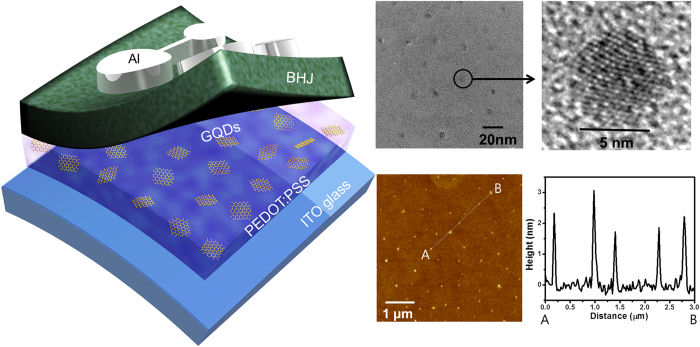
Figure 1 displays transmission electron microscope (TEM) and atomic force microscope (AFM) images of as-synthesized GQDs with uniform diameter of ~5 nm. The height of GQDs were ~2 nm, which reflect the number of layers in GQDs was approximately 3–4 layers, as evident from the AFM line profile. Fourier Transform Infrared Spectroscopy (FT-IR) and X-ray Photoelectron Spectroscopy (XPS) measurements were carried out to determine the composition of GQDs. Figure 2A shows FT-IR spectrum of GQDs in the range of 4000 ~ 400 cm−1, and exhibits the characteristic absorption bands corresponding to the stretching and bending vibration of -OH groups at 3452 cm−1, C=C stretching at 1637 cm−1, O-H deformation vibration at 1384 cm−1, phenolic hydroxyl group stretching of C-OH groups at 1265 cm−1, C-O vibration groups at 1095 cm−1, and epoxy stretching vibration of C-O-C groups at 1049 cm−1. In the C1s XPS spectrum of GQDs in Fig. 2B, three different peaks were decomposed, centered at 284.7, 286.4 and 288.2 eV, corresponding to sp2 carbon aromatic rings (C=C), C-O and C=O, respectively. The distinguished C-O and C=O peaks imply that the oxygen-related functional groups such as hydroxyl and carboxyl groups are on the edges of GQDs. Therefore, the functionalities could contribute to the dispersion of GQDs in polar solvents. In order to incorporate the GQDs into the PEODT:PSS solution, as-synthesized GQDs were blended in methanol, and were mixed with the PEDOT:PSS solution. The methanol does not have significantly negative effects on device performances, because it has been widely used as an additive or co-solvent for the PEDOT:PSS layer to improve the film morphology37.
Figure 1. Schematic of device, and TEM and AFM images of GQDs.
Schematic of OPV device with a GQD-incorporated PEDOT:PSS layer, and TEM images of the GQDs. The scale bar is 20 nm on the TEM image, and 5 nm on the inset image. AFM image of GQDs (5 μm by 5 μm) and height distribution from A to B.
Figure 2. Characteristics of GQDs.
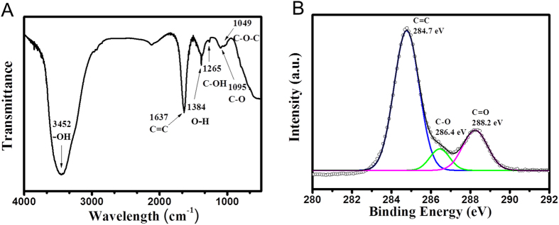
FT-IR (A) and XPS C1s (B) spectra of GQDs.
Surface morphologies of the GQDs-incorporated PEDOT:PSS film
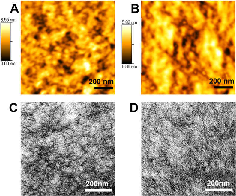
GQD-incorporated PEDOT:PSS layers were prepared by incorporating the GQDs/methanol solution in the PEDOT:PSS solution with varying weight ratio from 0.2 to 0.8 wt.%. Optimum device efficiency of 8.17% was accomplished by incorporating 0.4 wt.% of GQDs into the PEDOT:PSS layer as shown in supplementary Fig. S1 online. Though significantly lower quantity of GQDs were used in this study comparing to those of other metal nanomaterials in previous reports, GQDs comparably improved the device performance12,13,14,15,16,17,18,22,23. Figure 3 and Supplementary Fig. S2 online show the AFM images of GQDs incorporated into PEDOT:PSS films. GQDs were well dispersed in the PEDOT:PSS layer without any significant cracks, due to the high dispersion of GQDs in polar solvents. After the GQDs-incorporated PEDOT:PSS film was formed on the ITO substrate via spin-coating, OPV devices were fabricated following the conventional procedures. Figure 3A,B show AFM topography images of the PEDOT:PSS films w/o and w/GQDs, respectively. In a bare PEDOT:PSS, because it is difficult to form a uniform PEDOT layer on a substrate, the negatively charged PSS is doped in the positively charged PEDOT to enhance the dispersion property in polar solvent. The insulating PSS domains surround the highly conducting PEDOT domains, thereby the grain of PEDOT:PSS is composed of PEDOT-rich core and PSS-rich shell38,39,40,41,42. In addition, the grain size of PEDOT:PSS is usually determined by hydrogen bonds between PSS-rich shells43. Figure 3B indicates that the grain size of GQDs-incorporated PEDOT:PSS film is outstandingly increased while the grain boundaries are spread out more evenly. The GQDs with sufficient oxygen based functionalities intervene in the domain formation between PEDOT and PSS to determine the morphology of PEDOT:PSS film. The negatively charged GQDs can increase the size of PEDOT-rich cores because the positively charged PEDOT polymers combine with GQDs (Supplementary Fig. S3 online). Thereby, the decreased net charge of PEDOT results in lowering the electrostatic interaction between PEDOT-rich and PSS-rich domains. In addition, we obtained Cs-corrected TEM images as shown in Fig. 3C,D in order to understand the positive effects of GQDs in terms of the morphology properties. Unfortunately, it was difficult to visualize their domain structures from the Cs-corrected TEM images because all the components in the PEDOT:PSS layer has similar atoms. However, we observed that the skein-like black wires, which presumably indicated grain boundaries, were untangled in Fig. 3D when compared with Fig. 3C (without GQDs). This results indicate that grain size of PEDOT:PSS film was increased because of the interaction between PEDOT and the incorporated GQDs. The grain size of both PEDOT:PSS films with or without GQDs were quantified using a line measurement with AFM images in Supplementary Fig. S4 online.
Figure 3. AFM and TEM images of PEDOT:PSS film.
AFM images of PEDOT:PSS films without GQDs (A) and incorporating GQDs (B), which were spin coated on top of the ITO glass. Spherical aberration corrected transmission electron microscopy (Cs-corrected TEM) images of PEDOT:PSS film without (C) and with (D) GQDs. GQD concentration was 0.4 wt.%
Photovoltaic performance of the OPVs
The GQDs-incorporated device exhibits considerably improved PCE. Here, the PCE was determined by the intensity of power that a device generates using a given power of solar light at the maximum power.
 |
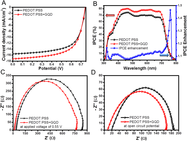
Among the parameters in this study, Jsc was significantly improved from 15.6 mA/cm2 to 17.3 mA/cm2 as shown in Fig. 4A,B, and Table 1. We confirmed that the enhanced Jsc was dominantly contributed to the improvement of PCE of the GQDs-incorporated PEDOT:PSS device (GQDs in HTL) through the incident photon to current conversion efficiency (IPCE) measurement. IPCE is defined by the number of injected electrons from the excited cites under the monochromatic light divided by pre-defined input photon flux. Hence, the external quantum efficiency (EQE) can be determined by IPCE measurement. Moreover, the Jsc parameter is estimated after integrating all the photocurrent density values obtained from IPCE measurement since the values are plotted as a function of each wavelength44.
Figure 4. Device performance and characterization.
Current vs. potential (J-V) curves (A), and incident photon-to-charge-carrier-efficiency (IPCE) and IPCE enhancement factor for the devices (B). Nyquist plots of electrochemical impedance spectroscopy at 0.55 V (C) and at open circuit potential (D). 0.4 wt.% of GQDs was incorporated into PEDOT:PSS layer.
Table 1. Performance parameters of the reference device with plain hole transporting layer (HTL, PEDOT:PSS), and the GQDs device composed of GQDs incorporated HTL and rGQD device composed of reduced GQDs incorporated HTL.
| Voc (V) | Jsc (mA/cm2) | FF (%) | PCEa (%) | Rshb (KΩcm2) | |
|---|---|---|---|---|---|
| Reference | 0.746 (±0.001) | 15.6 (±0.01) | 64.8 (±0.13) | 7.52 (±0.08) | 12.2 |
| GQDs in HTLc | 0.741 (±0.001) | 17.3 (±0.03) | 64.0 (±0.16) | 8.17 (±0.08) | 8.57 |
| rGQDs in HTLd | 0.719 (±0.012) | 15.9 (±0.05) | 65.4 (±0.21) | 7.48 (±0.14) | 18.8 |
| rGQDs in BHJe | 0.748 (±0.002) | 15.5 (±0.05) | 71.8 (±0.20) | 8.34 (±0.05) | 17.4 |
| GQDs in HTL/rGQDs in BHJ | 0.744 (±0.002) | 16.9 (±0.08) | 68.9 (±0.18) | 8.67 (±0.10) | 11.5 |
aThe device performance was average, as measured by six devices. To determine the cell area, the circular aperture (11.43 mm2) was used on top of the active area (15.71 mm2).
bThe shunt resistance values were obtained by using a same calculation process with our previous report52.
cThe 0.4 wt.% of GQDs was incorporated into PEDOT:PSS.
dThe 0.05 wt.% of rGQDs was incorporated into PEDOT:PSS.
eThe 0.02 wt.% of rGQDs was incorporated into BHJ.
 |
The jph and Pmono indicate experimentally obtained photocurrent value and power intensity of monochromatic incident light of a particular wavelength λ, respectively.
To understand the enhancement of Jsc, the electrochemical impedance spectroscopy (EIS) analysis was carried out as shown in Fig. 4C,D. In the Nyquist plot, the resistance value of the lowest point in the semicircle (near to 0 Ω) is related to the resistance of the both sides of electrodes (anode and cathode) and their interfaces45,46. In this study, we consider that the reduced resistance value at the lower resistance region resulted from the improved carrier conductance in the ITO/PEDOT:PSS, because there were no changes in the BHJ/cathode part45,46. The increased PEDOT-rich grains bring about improvement in the current paths and enhancement in the charge conductance37,38,39,40,41,42. Therefore, the hole transport performance of PEDOT:PSS layer with GQDs were improved due to the enhanced efficiency of the charge extraction from the BHJ layer, which resulted in the enhancement of Jsc parameter47.
Although GQDs absorb visible region in the solar spectrum, the incorporation of GQDs hardly affects the transmittance of PEDOT:PSS layer. Supplementary Fig. S5 B online shows the negligible changes in absorbance of PEDOT:PSS layer between w/o and w/GQDs. The diffuse reflectance data of GQDs/PEDOT:PSS films is slightly enhanced at visible region above 550 nm of solar spectrum (Supplementary Fig. S5 online). In addition, the incorporation of GQDs reduce the overall reflectance of OPV devices (ITO/PEDOT:PSS/BHJ/TiOx/Al) when the incident light is irradiated from the ITO glass side. This reveals that the incident light path from anode to BHJ layer was not disrupted when 0.4 wt.% of GQDs were incorporated into the PEDOT:PSS layer. The IPCE data, in Fig. 4B, shows that the adding of GQDs in the PEDOT:PSS increased the IPCE values in the wavelength range of 300 nm to 800 nm. The IPCE enhancement curve also displays that the increase of wavelength above 550 nm was slightly larger than at shorter wavelength, which results are well matched with the reflectance data in Supplementary Fig. S5 C and D online. This suggests that the improved IPCE result is in reliance with the scattering effect. Unlike the conventional metal-nanoparticle-embedded PEDOT:PSS hole extraction layers, we could neglect the SPR effect on GQDs despite their large amount of electron density. From the calculated E-field intensity distribution of a single Au nanoparticle and GQD, considerable plasmonic effects in the PEDOT:PSS layer with GQDs were not observed (Supplementary Fig. S6 online). Furthermore, the dramatically changed surface morphology of the GQDs-incorporated PEDOT:PSS elongates the incident light path in the device due to the relative index of GQDs (n = 1.6 and k = 0.02 at 600 nm of wavelength)15,16,17,18,48; this phenomenon is less dominant in the device compared to the morphological tuning effect of the PEDOT:PSS layer.
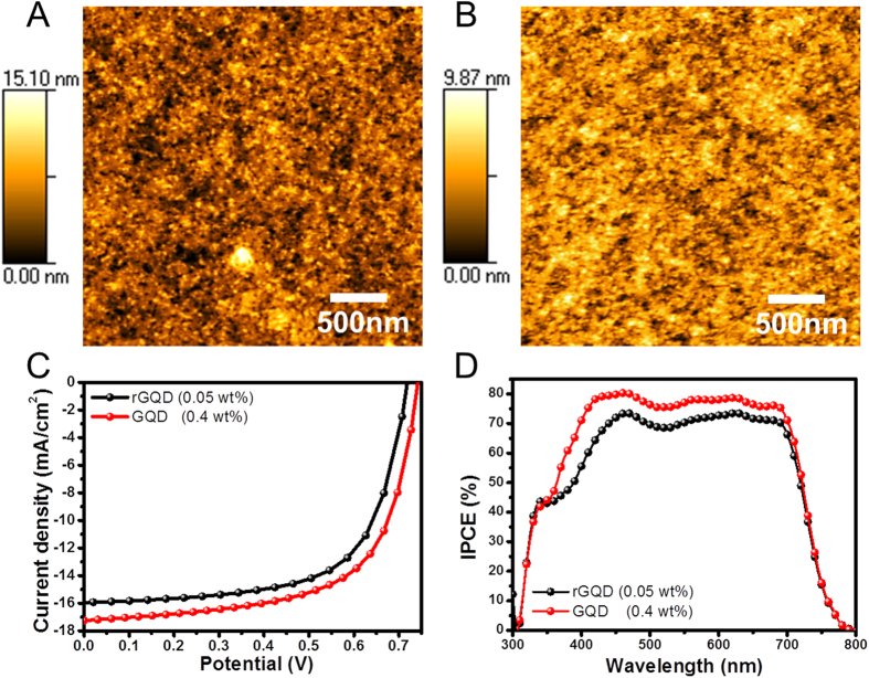
Nevertheless the charge conductance and the light harvesting performance were improved with GQDs, the fill factor of GQDs in HTL device was slightly lower than the reference device. This is because of the unconformable energy levels of GQDs as shown in Supplementary Fig. S7 online and slightly low Rsh value49,50 in Table 1. However, this negative effect of GQDs can be overcome by improving the morphological characteristics of composite film, which was confirmed by comparing the dispersion of as-synthesized GQDs and hydrothermally deoxidized rGQDs in the PEDOT:PSS film (Fig. 5)24. Previously, it was demonstrated that the oxygen-based moiety signals in XPS or FT-IR were strongly related to the quantitativeness of surface oxygen related functional groups of GQDs. From XPS measurement in Supplementary Fig. S8 online, GQDs contain a much stronger oxygen-based moiety signals than rGQDs. The hydrothermal method caused preponderant sp2 carbons in rGQDs so that the oxygen based functionalities of rGQDs were reduced. As shown in AFM images in Fig. 5A,B, even though the amount of rGQDs incorporated into PEDOT:PSS film was 20 times less than GQDs, the aggregated particles were much more observed on the surface of rGQDs-incorporated PEDOT:PSS film. As a result, the device performances might also strongly depend on the film quality of PEDOT:PSS layer as shown in Fig. 5. The rGQD incorporated device optimization information was described in Supplementary Fig. S9 and S10 online.
Figure 5. AFM and device performance in comparison with rGQD and GQDs in PEDOT:PSS.
AFM images of PEDOT:PSS films incorporating 0.05 wt.% of rGQDs (A) and 0.4 wt.% of GQDs (B).Current vs. potential (J-V) curves (C), and incident photon-to-charge-carrier-efficiency (IPCE) (D) for the devices.
Synergistically improved PCE of the OPVs by incorporating GQDs into the polymer layers
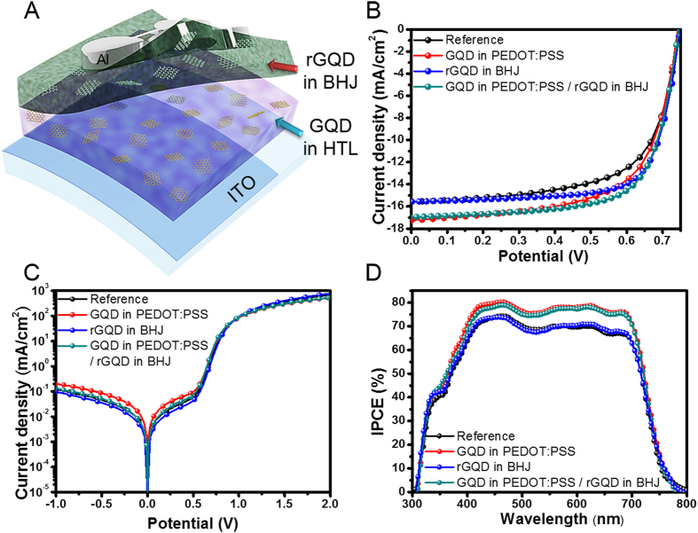
In our previous results, embedding the rGQDs in BHJ layers have enhanced the device performances of OPVs24. To take advantage of the synergistic effects, GQDs and rGQDs were placed in the PEDOT:PSS layer and the BHJ layer, respectively. Figure 6A shows a schematic illustration of the device with the rGQDs-incorporated BHJ film, which was coated on the GQDs-incorporated PEDOT:PSS film. The PCE value of the device composed of the BHJ layer with rGQD and bare PEDOT:PSS (rGQDs in BHJ device) was increased by about 10% as shown in Table 1. The FF was increased from 64.8% for reference device to 71.8% for rGQDs in BHJ device due to the improved carrier conductance and reduced resistance factors. The outstanding synergistic effects were observed in the device with the rGQDs-incorporated BHJ layer and the GQDs-incorporated PEDOT:PSS layer (GQD in PEDOT:PSS/rGQD in BHJ device), representing 8.67% PCE, resulting in 13% increase. The Jsc parameter was improved simultaneously with FF parameter. This result reveals that the positive effects from GQDs and rGQDs on the device educe the synergistic enhancement of the OPV performance without impeding each other.
Figure 6. Device performance of rGQDs and GQDs incorporated OPVs.
(A) Schematic illustration of the device with rGQDs in BHJ layer and GQDs in HTL (PEDOT:PSS), (B) J-V curves, (C) dark J-V curves and (D) IPCE of the devices with plain PEDOT:PSS and BHJ (black), PEDOT:PSS with GQDs (red), BHJ with rGQDs (blue) and GQDs and rGQDs incorporated PEDOT:PSS and BHJ (green). The concentration ratios of GQDs and rGQDs were 0.4 wt.% and 0.02 wt.% respectively.
In summary, the hydrophilic GQDs simply derived from carbon fibers were successfully incorporated into the PEDOT:PSS layer of an polymer BHJ photovoltaic device to enhance the power conversion efficiency. The high dispersibility of GQDs in polar solvents such as methanol allowed homogeneous incorporation of GQDs in hydrophilic PEDOT:PSS solution. The incorporation of GQDs with the sufficient oxygen based functionalities led to a significant morphological changes in PEDOT:PSS layer that improved the carrier conductance. Moreover, the GQDs-incorporation induced PEDOT:PSS layer extended light scattering and light confinement inside the OPV device. Taking these advantages of using GQDs in OPVs, the Jsc value has been increased by 10%. In addition to the incorporation of GQDs in the hole extraction layer, hydrophobic GQDs that were thermally reduced (rGQD) were hybridized in a bulk-heterojunction layer, which synergistically improved the PCE of OPV devices up to 8.67%.
Methods
Synthesis of Graphene Quantum Dots and Reduced Graphene Quantum Dots
GQDs were synthesized by acidic treatments of carbon fiber with 20 ml of HNO3 and 60 ml of H2SO4, and a thermal reaction at 120 °C36. After stirred for 24 hours, the mixture was diluted with 800 ml deionized water and neutralized by the addition of Na2CO3 to obtain a near pH 7. The reduced GQDs (rGQDs) were fabricated by using hydrothermal cutting methods from GOs24. The purified GOs, synthesized by the modified Hummer’s method, were treated using thermal reduction at 250 °C for 2 h. The graphite powder was dissolved in an acid solution composed of sulphuric acid and nitric acid to oxidize. After mild sonication for 1 day and dilution in distilled water, the solution was centrifuged for 30 min at 4000 rpm. The rinsing process, dilution and centrifugation, were repeated six times and the rinsed RGO was hydrothermally reduced 200 °C for 10 h to fabricate the rGQDs. After the obtained GQDs and rGQDs solutions were filtered with a 20 nm porous anodisc, it were dialyzed for 3 days to obtain the purified GQDs and rGQDs using a 2000 Da dialysis bag, respectively. Finally, the GQDs were re-dispersed in the methanol solvent for incorporating into the PEDOT:PSS layer. In addition, before preparing the BHJ with rGQDs solution, the rGQDs was re-dispersed in the chlorobenzene solvent.
Fabrication of OPVs
The hole extraction layer was prepared by incorporating GQDs into PEDOT:PSS (AI4083, Clevious) solution with various weight ratios. The total quantity of methanol used as a co-solvent was same in the all PEDOT:PSS solution. A 40 nm thick PEDOT:PSS layer was spin-cast on a pre-cleaned ITO glass and then dried at 150 °C for 15 min. After that, an 80 nm thick layer of BHJ was spin-coated in an Ar filled glove box. The BHJ solution composed of PTB7 (1-Material Chemscitech Inc., Lot #:YY5220) and PC71BM (Nano-c) with 1:1.5 of weight ratio was prepared to 2.5 wt.% in 3% of 1,8-diiodooctane mixed chlorobenzene solvent. In the case of preparatory for devices with rGQDs/BHJ layer, 0.02 wt.% of rGQDs was blended in the BHJ solution. Then, approximately 6 nm of TiOx interlayer was spin-coated for electron conducting layer and a 120 nm thick Aluminum metal cathode was deposited by thermal evaporation at ~10−7 Torr.
Characterization
The AFM images for GQDs were measured by noncontact mode with a Park System XE-100 atomic force microscope. The TEM images were obtained with a JEOL JEM-3010 electron microscope operating at 300 kV and Spherical aberration corrected transmission electron microscopy (Cs-corrected TEM) images were obtained with a JEOL JEM ARM 200 F. In order to prepare the samples for TEM measurement, pre-formed PEDOT:PSS layer was stamping-transferred on a TEM grid by a dry-transfer method with a rigiflex polyurethane acrylate coated polycarbonate (PUA/PC) mold as previously reported method47,51. The FT-IR spectra were obtained by using a Thermo Scientific Nicolet 6700 spectrometer. XPS analysis was carried out with a Thermo Scientific K-Alpha small-spot X-ray Photoelectron Spectrometer (XPS) system. We prepare our GQD samples for FT-IR and XPS measurements by using the same method with our previous report24. The surface topology images of PEDOT:PSS were investigated using atomic force microscopy (AFM, Dimension 3100, Veeco, Plainview, NY) in tapping mode. The absorption and reflectance were obtained using a UV-vis spectrophotometer (UV-3600, Shimadzu). The diffuse reflectance was measured using UV-vis spectrophotometer (Cary 5000) equipped with an integrating sphere accessory. The J-V device performances were measured by a solar simulator (Oriel 91193, 1000 W lamp with 100 mW/cm2) using an NREL-calibrated Si solar cell and Keithley 2400 source meters. The incident photon-to-current efficiency (IPCE) measurements were performed by using a Solar Cell QE/IPCE Measurement (Zolix Solar Cell Scan 100).
Additional Information
How to cite this article: Kim, J. K. et al. Surface-Engineered Graphene Quantum Dots Incorporated into Polymer Layers for High Performance Organic Photovoltaics. Sci. Rep. 5, 14276; doi: 10.1038/srep14276 (2015).
Supplementary Material
Acknowledgments
This research was supported by the Basic Science Research Program (NRF-2013R1A2A1A09014038, 2011-0030254, 2011-00006286, 2014M3A7B4051747, 2011-0017587), the Global Ph.D fellowship program (NRF-2012H1A2A1016034), the Global Research Lab (GRL) Program (2011-0021972), and the Global Frontier Research Program (2011-0031629) through the National Research Foundation of Korea (NRF) funded by the Korean government (MEST and MKE). B. H. H. appreciates the financial support from the SBS foundation. Institutional Program. S. Bae appreciates the financial support from the Korea Institute of Science and Technology (KIST) Institutional Program (2Z04420) and the Graphene Materials/Components Development Project (10044366) through the Ministry of Trade, Industry, and Energy (MOTIE), Republic of Korea.
Footnotes
Author Contributions J.K.K. deceived the idea, designed the device structure and fabricated the device. S.J.K. synthesized GQDs and conducted F.T.-I.R. and X.P.S. measurements. M.J.P. assisted the experiments and GQD characterization. S.B. advised the synthesis and characterization of GQDs. S.-P.C. conducted TEM measurement. Q.G.D. performed optical calculation. D.H.W. advised the device characterization. Two corresponding authors J.H.P. and B.H.H. supervised this work. J.K.K., S.J.K., J.H.P. and B.H.H. took part in writing the manuscript.
References
- Sariciftci N. S., Smilowitz L., Heeger A. J. & Wudl F. Photoinduced Electron Transfer from a Conducting Polymer to Buckminsterfullerene. Science 258, 1474–1476 (1992). [DOI] [PubMed] [Google Scholar]
- Yu G., Gao J., Hummelen J. C., Wudl F. & Heeger A. J. Polymer Photovoltaic Cells: Enhanced Efficiencies via a Network of Internal Donor-Acceptor Heterojunctions. Science 270, 1789–1791 (1995). [Google Scholar]
- Heeger A. J. Semiconducting and Metallic Polymers: The Fourth Generation of Polymeric Materials. Angew. Chem., Int. Ed. 40, 2591–2611 (2001). [DOI] [PubMed] [Google Scholar]
- Blom P. W. M., Mihailetchi V. D., Koster L. J. A. & Markov D. E. Device Physics of Polymer:Fullerene Bulk Heterojunction Solar Cells. Adv. Mater. 19, 1551–1566 (2007). [Google Scholar]
- Markov D. E., Amsterdam E., Blom P. W. M., Sieval A. B. & Hummelen J. C. Accurate Measurement of the Exciton Diffusion Length in a Conjugated Polymer Using a Heterostructure with a Side-Chain Cross-Linked Fullerene Layer. J. Phys. Chem. A 109, 5266–5274 (2005). [DOI] [PubMed] [Google Scholar]
- Wang D. H. et al. Sequential Processing: Control of Nanomorphology in Bulk Heterojunction Solar Cells. Nano Lett. 11, 3163–3168 (2011). [DOI] [PubMed] [Google Scholar]
- Hoven C. V. et al. Improved Performance of Polymer Bulk Heterojunction Solar Cells Through the Reduction of Phase Separation via Solvent Additives. Adv. Mater. 22, E63–E66 (2010). [DOI] [PubMed] [Google Scholar]
- Ma W., Yang C., Gong X., Lee K. & Heeger A. J. Thermally Stable, Efficient Polymer Solar Cells with Nanoscale Control of the Interpenetrating Network Morphology. Adv. Funct. Mater. 15, 1617–1622 (2005). [Google Scholar]
- Brabec C. J., Sariciftci N. S. & Hummelen J. C. Plastic Solar Cells. Adv. Funct. Mater. 11, 15–26 (2001). [Google Scholar]
- Wang D. H., Choi D.-G., Lee K.-J., Park O. O. & Park J. H. Photovoltaic Devices with an Active Layer from a Stamping Transfer Technique: Single Layer Versus Double Layer. Langmuir 26, 9584–9588 (2010). [DOI] [PubMed] [Google Scholar]
- Wang D. H. et al. Unexpected solid–solid intermixing in a bilayer of poly(3-hexylthiophene) and [6,6]-phenyl C61-butyric acidmethyl ester via stamping transfer. Org. Electron. 11, 1376–1380 (2010). [Google Scholar]
- Atwater H. A. & Polman A. Plasmonics for improved photovoltaic devices. Nat. Mater. 9, 205–213 (2010). [DOI] [PubMed] [Google Scholar]
- Wang D. H. et al. Enhanced Power Conversion Efficiency in PCDTBT/PC70BM Bulk Heterojunction Photovoltaic Devices with Embedded Silver Nanoparticle Clusters. Adv. Energy Mater. 1, 766–770 (2011). [Google Scholar]
- Wang D. H. et al. Enhancement of Donor–Acceptor Polymer Bulk Heterojunction Solar Cell Power Conversion Efficiencies by Addition of Au Nanoparticles. Angew. Chem., Int. Ed. 50, 5519–5523 (2011). [DOI] [PubMed] [Google Scholar]
- Wang D. H. et al. Enhanced light harvesting in bulk heterojunction photovoltaic devices with shape-controlled Ag nanomaterials: Ag nanoparticles versus Ag nanoplates. RSC Adv. 2, 7268–7272 (2012). [Google Scholar]
- Lu L., Luo Z., Xu T. & Yu L. Cooperative Plasmonic Effect of Ag and Au Nanoparticles on Enhancing Performance of Polymer Solar Cells. Nano Lett. 13, 59–64 (2012). [DOI] [PubMed] [Google Scholar]
- Baek S.-W. et al. Plasmonic Forward Scattering Effect in Organic Solar Cells: A Powerful Optical Engineering Method. Sci. Rep. 3, 1726 (2013). [Google Scholar]
- Ko S.-J. et al. Highly efficient plasmonic organic optoelectronic devices based on a conducting polymer electrode incorporated with silver nanoparticles. Energy Environ. Sci. 6, 1949–1955 (2013). [Google Scholar]
- Liu H., Goh W.-P., Leung M.-Y., Li Y. & Norsten T. B. Effect of Nanoparticle Stabilizing Ligands and Ligand-Capped Gold Nanoparticles in Polymer Solar Cells. Sol. Energy Mater. Sol. Cells 96, 302 (2012). [Google Scholar]
- Wu B. et al. Uncovering Loss Mechanisms in Silver Nanoparticle-Blended Plasmonic Organic Solar Cells. Nat. Commun. 4, 2004 (2013). [DOI] [PubMed] [Google Scholar]
- Xue M. et al. Charge-carrier dynamics in hybrid plasmonic organic solar cells with Ag nanoparticles. Appl. Phys. Lett. 98, 253302 (2011). [Google Scholar]
- Janković V. et al. Active layer-incorporated, spectrally tuned Au/SiO2 core/shell nanorod-based light trapping for organic photovoltaics. ACS Nano 7, 3815–3822 (2013). [DOI] [PubMed] [Google Scholar]
- Choi H. et al. Multipositional Silica-Coated Silver Nanoparticles for High-Performance Polymer Solar Cells. Nano Lett. 13, 2204–2208 (2013). [DOI] [PubMed] [Google Scholar]
- Kim J. K. et al. Balancing Light Absorptivity and Carrier Conductivity of Graphene Quantum Dots for High-Efficiency Bulk Heterojunction Solar Cells. ACS Nano 7, 7207–7212 (2013). [DOI] [PubMed] [Google Scholar]
- Li Y. et al. An Electrochemical Avenue to Green-Luminescent Graphene Quantum Dots as Potential Electron-Acceptors for Photovoltaics. Adv. Mater. 23, 776–780 (2011). [DOI] [PubMed] [Google Scholar]
- Gupta V. et al. Luminscent Graphene Quantum Dots for Organic Photovoltaic Devices. J. Am. Chem. Soc. 133, 9960–9963 (2011). [DOI] [PubMed] [Google Scholar]
- Shen J., Zhu Y., Yang X. & Li C. Graphene quantum dots: emergent nanolights for bioimaging, sensors, catalysis and photovoltaic devices. Chem. Commun. 48, 3686–3699 (2012). [DOI] [PubMed] [Google Scholar]
- Wang X., Zhi L. & Mullen K. Transparent, Conductive Graphene Electrodes for Dye-Sensitized Solar Cells. Nano Lett. 8, 323–327 (2008). [DOI] [PubMed] [Google Scholar]
- Eda G., Fanchini G. & Chhowalla M. Large-area ultrathin films of reduced graphene oxide as a transparent and flexible electronic material. Nat. Nanotechnol. 3, 270–274 (2008). [DOI] [PubMed] [Google Scholar]
- Robinson J. T., Perkins F. K., Snow E. S., Wei Z. & Sheehan P. E. Reduced Graphene Oxide Molecular Sensors. Nano Lett. 8, 3137–3140 (2008). [DOI] [PubMed] [Google Scholar]
- Robinson J. T. et al. Wafer-scale Reduced Graphene Oxide Films for Nanomechanical Devices. Nano Lett. 8, 3441–3445 (2008). [DOI] [PubMed] [Google Scholar]
- Eda G. et al. Transparent and conducting electrodes for organic electronics from reduced graphene oxide. Appl. Phys. Lett. 92, 233305 (2008). [Google Scholar]
- Park S. & Ruoff R. S. Chemical methods for the production of graphenes. Nat. Nanotechnol. 4, 217–224 (2009). [DOI] [PubMed] [Google Scholar]
- Becerril H. A. et al. Evaluation of Solution-Processed Reduced Graphene Oxide Films as Transparent Conductors. ACS Nano 2, 463–470 (2008). [DOI] [PubMed] [Google Scholar]
- Zhu Z. et al. Efficiency Enhancement of Perovskite Solar Cells through Fast Electron Extraction: The Role of Graphene Quantum Dots. J. Am. Chem. Soc. 136, 3760–3763 (2014). [DOI] [PubMed] [Google Scholar]
- Peng J. et al. Graphene Quantum Dots Derived from Carbon Fibers. Nano Lett. 12, 844–849 (2012). [DOI] [PubMed] [Google Scholar]
- Sun K., Xia Y. & Ouyang J. Improvement in the photovoltaic efficiency of polymer solar cells by treating the poly(3,4-ethylenedioxythiophene): poly(styrenesulfonate) buffer layer with co-solvents of hydrophilic organic solvents and hydrophobic 1,2-dichlorobenzene. Sol. Energy Mater. Sol. Cells 97, 89–96 (2012). [Google Scholar]
- Jönsson S. K. M. et al. The effects of solvents on the morphology and sheet resistance in poly(3,4-ethylenedioxythiophene)–polystyrenesulfonic acid (PEDOT–PSS) films. Synth. Met. 139, 1–10 (2003). [Google Scholar]
- Nardes A. M., Janssen R. A. J. & Kemerink M. A Morphological Model for the Solvent-Enhanced Conductivity of PEDOT:PSS Thin Films. Adv. Funct. Mater. 18, 865–871 (2008). [Google Scholar]
- Ouyang J., Chu C. W., Chen F. C., Xu Q. & Yang Y. High-Conductivity Poly(3,4-ethylenedioxythiophene):Poly(styrene sulfonate) Film and Its Application in Polymer Optoelectronic Devices. Adv. Funct. Mater. 15, 203–208 (2005). [Google Scholar]
- Kim Y. H. et al. Highly Conductive PEDOT:PSS Electrode with Optimized Solvent and Thermal Post-Treatment for ITO-Free Organic Solar Cells. Adv. Funct. Mater. 21, 1076–1081 (2011). [Google Scholar]
- Yeo J. S., Yun J. M., Kim D. Y., Kim S. S. & Na S. I. Successive solvent-treated PEDOT:PSS electrodes for flexible ITO-free organic photovoltaics. Sol. Energy Mater. Sol. Cells 114, 104–109 (2013). [Google Scholar]
- Lang U., Müller E., Naujoks N. & Dual J. Microscopical Investigations of PEDOT:PSS Thin Films. Adv. Funct. Mater. 19, 1215 (2009). [Google Scholar]
- Grätzel M. Recent Advances in Sensitized Mesoscopic Solar Cells. Acc. Chem. Res. 42, 1788 (2009). [DOI] [PubMed] [Google Scholar]
- Zhou H. et al. High-Efficiency Polymer Solar Cells Enhanced by Solvent Treatment. Adv. Mater. 25, 1646–1652 (2013). [DOI] [PubMed] [Google Scholar]
- Leever B. J., Bailey C. A., Marks T. J., Hersam M. C. & Durstock M. F. In Situ Characterization of Lifetime and Morphology in Operating Bulk Heterojunction Organic Photovoltaic Devices by Impedance Spectroscopy. Adv. Energy Mater. 2, 120–128 (2012). [Google Scholar]
- Kim J. K. et al. Enhanced performance and stability of polymer BHJ photovoltaic devices from dry transfer of PEDOT:PSS. Chemsuschem 7, 1957–1963 (2014). [DOI] [PubMed] [Google Scholar]
- Kim W. et al. Polymer Bulk Heterojunction Solar Cells with PEDOT:PSS Bilayer Structure as Hole Extraction Layer. ChemSusChem 6, 1070–1075 (2013). [DOI] [PubMed] [Google Scholar]
- Lee T. W., Park O. O., Yoon J. & Kim J. J. Polymer-Layered Silicate Nanocomposite Light-Emitting Devices. Adv. Mater. 13, 211–213 (2001). [Google Scholar]
- Kim J. K. et al. Ultrathin nanoclay films with tunable thickness as barrier layers in organic light emitting devices. J. Mater. Chem. 22, 7718–7723 (2012). [Google Scholar]
- Kim J. K., Veerappan G., Heo N., Wang D. H. & Park J. H. Efficient Hole Extraction from Sb2S3 Heterojunction Solar Cells by the Solid Transfer of Preformed PEDOT:PSS Film. J. Phys. Chem. C 118, 22672–22677 (2014). [Google Scholar]
- Wang D. H. et al. Transferable Graphene Oxide by Stamping Nanotechnology: Electron-Transport Layer for Efficient Bulk-Heterojunction Solar Cells. Angew. Chem. Int. Ed. 125, 2946–2952 (2013). [DOI] [PubMed] [Google Scholar]
Associated Data
This section collects any data citations, data availability statements, or supplementary materials included in this article.


