

Abstract
We investigate instability mechanisms in amorphous In-Ga-Zn-O transistors based on bias and illumination stress-recovery experiments coupled with analysis using stretched exponentials and inverse Laplace transform to retrieve the distribution of activation energies associated with metastable oxygen defects. Results show that the recovery process after illumination stress is persistently slow by virtue of defect states with a broad range, 0.85 eV to 1.38 eV, suggesting the presence of ionized oxygen vacancies and interstitials. We also rule out charge trapping/detrapping events since this requires a much smaller activation energy ~0.53 eV, and which tends to be much quicker. These arguments are supported by measurements using a novel gate-pulse spectroscopy probing technique that reveals the post-stress ionized oxygen defect profile, including anti-bonding states within the conduction band.
Transparent conducting oxides are promising candidate as channel material for thin film transistors (TFTs) due to their high electron mobility and optical transparency1,2,3. However, this class of materials shows persistent photoconductivity (PPC) even under visible illumination despite its wide band-gap ~3 eV4,5. Interestingly, PPC can give rise to high optical detectivity in oxide semiconductor-based photodetectors5,6,7,8,9. Thus its imperative that we understand the physical origin of PPC.
In order to explain the underlying mechanisms of PPC, there are two possible models. One relates to charge trapping (CT) and the other to oxygen defect ionization (ODI) (see Fig. 1(a)). With the former6,9, optically generated holes can be trapped at the gate insulator and its interface, and in defects in the oxide semiconductor layer (e.g., localized traps in an amorphous oxide structure, and grain boundary defects in nano-crystalline oxides). The trapped holes can induce electrons in the channel, yielding a negative threshold (VT) shift in the drain current (IDS) vs. gate-voltage (VGS) characteristics in an oxide TFT5,6,7,8,9,10. However, the PPC can also be explained with the ODI model. Here, a negative VT shift implies more electrons (e−) are created thereby increasing Fermi level (EF). These additional electrons (2e−) can originate from the ODI process in the form of metastable oxygen defects, such as oxygen vacancy ionization (VO0 → VO2+ + 2e−) and oxygen interstitial ionization (IO2− → IO0 + 2e−)5,7,8,9,10,11,12,13,14,15 (see Fig. 1(b)). These two ionization processes can be formulated commonly as D0/2− → D2+/0 + 2e−. The ionized oxygen defects (D2+/0) remain ionized since they are at a higher energy level compared to their previous states (D0/2−), as illustrated in Fig. 1(b). This makes the shift in VT persist, thus slowing down recovery and forming the physical basis of PPC. Thus the origin of illumination-induced instability (i.e. negative VT shift) can appear to be somewhat controversial between the CT and ODI mechanisms.
Figure 1.

Illustration of (a) instability mechanisms and (b) oxygen defect ionization (ODI) to explain persistent conductivity associated with the increased energy level of the ionized oxygen defect states under illumination stress.
This work attempts to clarify this controversy through a series of experiments and analyses using amorphous In-Ga-Zn-O (a-IGZO) TFTs. Firstly, the recovery behavior after illumination stress is measured independently and compared with the case after negative bias stress (NBS) in the dark. The latter is intended to promote the hole trapping16,17,18,19,20,21. Here, the bias and time of NBS are tuned to −20 V and 30 sec, respectively, to yield an equivalent value of negative VT shift when subject to illumination stress for 30 sec duration. It is found that the recovery behavior after illumination stress is very slow (i.e. persistent) whereas NBS leads to a fast recovery. This demonstrates that the instability with illumination stress cannot be dominated with the hole trapping.
Secondly, we studied activation energy distributions for stress and recovery with illumination stress and NBS, respectively. With the former, the TFT’s gate electrode was kept floating to minimize the vertical E-field which can be a source of hole trapping. To get the activation energy profile, we used a stretched exponential function to model stress and recovery characteristics as a function of time, and its inverse Laplace transform with the Arrhenius relation. As a key observation, the recovery process after illumination stress appears to happen through two different defect states. One defect state provides a much higher activation energy level compared to the other, which has a similar energy distribution with the recovery behaviour after NBS. These results indicate that the state located at the higher energy level is the main origin of the slow recovery and PPC. This further suggests that the recover process after illumination stress takes place through more deeply bound states, which can be explained with the ionized oxygen defect states.
We introduce a new probing technique based on gate-pulse spectroscopy (GPS) to capture the profile of these metastable oxygen defects, e.g. ionized oxygen defect states, as a function of energy. Here, a gate-pulse train with an incremental pulse height from 1 V to 13 V is applied for gradual recovery of VT. The amount of recovered VT can be correlated with the concentration of the ionized oxygen defects. Although the extent of recovered VT can also stem from electron trapping during the GPS procedure, we can subtract this using the values of VT shift obtained from an equivalent GPS procedure applied to a non-illuminated sample. Based on this, we find that the profile of the ionized oxygen defect states is distributed in the energy range from −1.25 eV to +0.07 eV. In particular, the states within the conduction band at 0 to +0.07 eV can be viewed as anti-bonding states (σ*) between the lattice oxygen and excess oxygen atoms (interstitials).
Finally, we argue that the proposed analysis and spectroscopy technique are useful to identify optical instability mechanisms in other oxide semiconductors such as Zn-O, Ga-O, and In-Zn-O.
Results and Discussion
A. Instability Observations
Figure 2(a) shows the measured drain current (IDS) as a function of gate voltage (VGS) at a drain voltage (VDS) of 1 V for two different cases, one is after NBS for 30 sec and the other after illumination stress for 30 sec, in comparison with the pre-stress case. Here, the level of NBS is limited to −20 V to get the same threshold voltage shift (ΔVT ~ −1.3 V) as with illumination stress at ~0.5 mW/cm2 optical power at 450 nm wavelength. At the same time, the corresponding drain current at VGS = 0 V, denoted as IDS0 (used as a reference to ΔVT), is increased up to 1 nA for both cases, as seen in Fig. 2(a). This is also seen in Fig. 2(b) at t = 0 sec in which both stresses are removed and recovery processes start with the condition of VGS = 0 V and VDS = 1 V. We see that the recovery after NBS is almost complete while the recovery after illumination stress shows a persistency (i.e. PPC) and almost saturating after 120 sec, although the initial decay is fast. This initial fast decay may be due to detrapping of holes that may have been trapped in the gate insulator or interface during illumination. It can be argued that the illumination-induced VT shift and PPC, as evidenced by the observed recovery, is not totally arising from the hole trapping.
Figure 2.

(a) Transfer characteristics at VDS = 1 V for the cases after NBS (at VG = −20 V) and illumination stress for 30 sec in comparison with the pre-stressed a-IGZO TFTs (Inset: Schematic cross-sectional view of the examined TFTs). The TFTs examined have channel length (L) = 4μm and width (W) = 100 μm with 100 nm thick SiO2 as the gate insulator. Both NBS and illumination stress lead to a negative ΔVT of −1.3 V, and IDS at VGS = 0 V (IDS0) is increased as an outcome of the negative VT shift. (b) Recovery behavior of IDS0 after illumination stress and NBS, respectively. (c) Measured conductance (GDS) as a function of time under illumination stress (photo-excitation) without gate probing as shown in the inset. (d) Measured GDS as a function of time time after illumination stress (recovery). (e) Measured ΔVT as a function of time under NBS (excitation). (f) Measured ΔVT as a function of time after NBS (recovery). Here, ΔVT values are retrieved from the IDS-VGS characteristics (at VDS = 1 V) measured with NBS at every 60 sec. After 300 sec of NBS, ΔVT values are retrieved from the IDS-VGS characteristics (at VDS = 1 V) measured without NBS at every 60 sec.
However, the fast and complete post-NBS recovery, as seen in Fig. 2(b,f)16, can be explained with the hole detrapping. To quantify this, the detrapping time (τd) for each hole can be estimated as17,
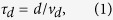 |
where d is the characteristic penetration depth at which traps are filled with holes, and νd the drift velocity for holes. Here, vd can be defined as vd = μh·Eeff = 3 × 104 cm/s, where the hole mobility μh ≈ 0.1 cm2/V·s16, and the transverse built-in electric field post NBS Eeff ≈ |ΔVT(0)|/tox = 3 × 10⁷ V/m for ΔVT(0) ≈ 3 V and thickness of gate insulator tox ≈ 100 nm. In Equation (1), d is defined as follows17, d = 1.15|ΔVT(0)|/(Kdrd). Here, the wave function decay constant Kd ~ 1010/m, and the decay rate rd ≈ 1.7 V/dec calculated as d|ΔVT(t)|/dlog(t) on the decay plot seen in Fig. 2(f), yielding d ≈ 0.2 nm. Finally, Eq.(1) gives τd ≈ 6.7 × 10⁻¹² sec, implying a fast recovery. In addition, it has been demonstrated that this fast recovery process of trapped holes is fast enough high frame rate active matrix organic displays18.
For the illumination stress experiments shown in Fig. 2(a,b), a vertical electric field (E-field) along the channel depth is induced by virtue of an applied positive gate bias. This E-field can give rise to charge trapping. To minimize the effect of the gate field and to extract a pure channel layer contribution to illumination-induced instability, the transient conductance (GDS) with the gate floating is measured with a fixed VDS = 5 V (see the inset of Fig. 2(c)). As seen in Fig. 2(c), the GDS under illumination stress is increased with time, suggesting an increase of the channel layer conductivity (σch) since GDS ≈ σchtchW/L, where tch is the channel thickness. After illumination stress for 300 sec, the recovery of GDS is also monitored, as seen in Fig. 2(d). Similar to Fig. 2(b), GDS is not completely recovered and shows PPC behavior. In contrast, the trend of ΔVT in post-NBS shows almost complete recovery with a behavior that is symmetric with that during NBS—see Fig. 2(e,f). To quantify the observed stress and recovery behaviour, a stretched exponential analysis is employed19,20. This is discussed in the following section.
B. Stretched Exponential Analysis
To model the transient stress and recovery characteristics, we use a stretched exponential function (SEF) of time (F(t)) as follows19,20,
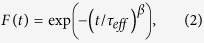 |
where τeff is an effective time constant and β a stretched exponent which is a real number bigger than zero. Note that normalized stress and recovery behavior can be represented as 1-F(t) and F(t), respectively, and the common term to explain each transient curvature is F(t) which mainly determines τeff and β. Based on Equation (2), the stress and recovery curves for both illumination stress and NBS can be modeled, yielding values of τeff and β for each case, as seen in Fig. 3(a–d) (see also the section S1 in the Supporting information). As expected, the post-NBS case shows good agreement with a single SEF, implying presence of a single mechanism, i.e. hole detrapping. In contrast, the post illumination stress case shows a piece-wise linear characteristic. Thus this recovery behavior should be modeled with two different SEFs, as shown in Fig. 3(d,e), implying presence of two independent mechanisms during post illumination stress recovery. The first SEF has τeff = 56 sec and β = 0.87, which are quite comparable with the post-NBS case, suggesting presence of a similar mechanism during the post illumination stress recovery process. At the same time, the second SEF yields a value of τeff = 4507 sec, which is larger compared to any other case, and β = 0.11. In particular, this large value of τeff implies the need for a much longer time period to finish recovery. This is reminiscent of persistent photoconductivity and an important bearing on the role of oxygen defects. The extracted values of τeff and β for each case are summarized in Table 1. With these values, we can now deduce an activation energy distribution.
Figure 3.

Excitation behavior modeled with SEF for (a) NBS and (b) illumination stress, respectively. Recovery behaviour modeled with SEF for (c) NBS and (d) illumination stress, respectively. (e) Recovery behaviour as a function of time for post illumination stress GDS modeled with two SEFs. Here, A1 and A2 are coefficients, and their sum equals to GDS-Max.
Table 1. Parameters Retrieved with a Stretched Exponential Function for NBS and Illumination Stress Cases.
| StressType | Excitation | Recovery | |||
|---|---|---|---|---|---|
| τeff | β | τeff | β | ||
| NBS | 59 sec | 0.87 | 61 sec | 0.81 | |
| LS | 315 sec | 0.82 | F1 | 56 sec | 0.87 |
| F2 | 4507 sec | 0.11 | |||
C. Activation Energy Distribution
To get an activation energy distribution function, as the first step, we need to find the frequency domain function, f(S), from the inverse Laplace transform (ILT) of F(t)21 defined as follows,
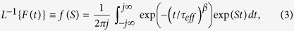 |
where S is a frequency. In order to convert this to an energy distribution function, the frequency parameter S needs to be replaced with activation energy (EA) using the Arrhenius relation,
 |
Here, νAE is an attempt-to-escape frequency and kT the thermal energy. Note that νAE is different from a lattice vibration frequency which is about 1013/sec22,23. Using a saddle point method along with Equation (4)24, the analytical solution of Equation (3) constitutes the activation energy distribution function, f(EA),
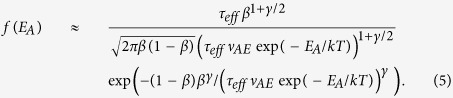 |
For the detailed derivation procedure, see the section S2 in the Supporting Information. In Equation (5), the main unknown is νAE. To retrieve the value of νAE, excitation state experiments under illumination stress are performed for different temperatures. This yields νAE = 107/sec (see section S3 in the Supporting Information), suggesting that the examined device has ~107/sec as an attempt-to-escape frequency, which is consistent with the value chosen in ref. 23.
With the extracted value of νAE, we can plot the activation energy distribution function f(EA) for each of the instability cases using Equation (5) using the respective values of τeff and β (see Table 1). Figure 4(a) shows the normalized f(EA) for NBS (excitation) and post-NBS (dark recovery) cases, respectively. The peak energy level (Epeak) under NBS is 0.52 eV, which is similar to that of the post-NBS, suggesting complete recovery in a similar time period. However, the cases of illumination stress (photo-excitation) and post illumination stress (dark recovery) are quite different from the NBS cases. As seen in Fig. 4(b), the post illumination stress has double peaks. In particular, it shows a much higher activation energy state (state 2) while state 1 is located near the excitation state. This implies that there are two different recovery processes. Since state 2 has a higher peak activation energy ~1.15 eV, it suggests that recovery is being processed through more deeply bound states20, and is consistent with the nature of the ionized metastable oxygen defects4,5,6,7,8,9,10,11,12. Here, we believe that the slow recovery after illumination stress, i.e. PPC, is due to the ionized oxygen defects, which needs a higher activation energy to be neutralized11,12. This is depicted in Fig. 4(c).
Figure 4.

Normalized f(EA) as a function of activation energy (EA) for (a) NBS (excitation) and post-NBS (dark recovery), and (b) illumination stress (photo-excitation) and post illumination stress (dark recovery), respectively. (c) Activation energy diagram for the cases of illumination stress (photo-excitation) and post illumination stress (dark recovery). Here, the ground state level is defined as an intrinsic Fermi level (EFi). (d) Deduced location of each state as a function of energy. In particular, State 2 has both states below and above the conduction band minima (EC).
Here, the ground state level, defined as an intrinsic Fermi level (EFi), is ~1.2 eV. The corresponding energy band diagram in Fig. 4(d) shows the location of each state as a function of energy. Here, the key observation is state 2 located on both sides of the conduction band minima (EC), in which states above EC are supposed to be an anti-bonding state associated with oxygen interstitials25.
D. Gate-Pulse Spectroscopy
For insight into the location of these defect states, we developed a new gate-pulse spectroscopy (GPS) technique which yields the DOS profile of the ionized metastable oxygen defects, e.g. ionized oxygen vacancies and interstitials. The GPS technique is applied after illumination stress. In particular, GPS allows us to compare the result shown in Fig. 4(d). Here, the basic idea is that the D2+/0 states become occupied when they are located below EF, hence enabling recombination with electrons, i.e. D2+/0 + 2e− → D0/2−, and hence the recovery of VT. If we vary the gate pulse height (VGPH) in small increments, the D2+/0 states become gradually occupied, as depicted in Fig. 5(a). As an outcome after each gate pulse, VT correspondingly recovers with a behavior that correlates with the density of ionized oxygen defects. Note that, besides oxygen defect recombination, it is also possible that there is electron trapping as an adverse effect while applying the GPS, as described in Fig. 5(a). After 60 sec illumination stress with 1 mW/cm2 optical source of 450 nm, the transfer characteristics show a negative VT shift which is almost saturated yielding |ΔVT| = 1.2 V after 240 sec from the time at which illumination stress ceases (i.e. start of recovery). Subsequently, we apply a gate-pulse train with varying pulse heights from 1 V to 13 V, as shown in Fig. 5(b). Here, the gate-pulse height (VGPH) is set as VGS–VFBe (where VFBe is an effective flat-band voltage at which IDS = 10−13 A). In our case, a complete recovery of VT is achieved after VGPH = 11 V, leading to a positive VT shift after every stage of the gate-pulse train. However, it is found that transfer curves after gate pulsing with VGPH ≥ 12 V are further shifted to a more positive direction compared to the pre-stressed case, as can be seen in Fig. 5(c), This implies presence of another mechanism stemming from the gate-pulse. Since the polarity of gate-pulse is positive, it may be due to the electron trapping (see Fig. 5(a)). This means the gate pulse-induced VT recovery after illumination stress (ΔVTRIS) should contain some degree of electron trapping at every stage of the gate-pulse train, as depicted in the inset of Fig. 5(c). To estimate this, we perform gate pulsing on non-illuminated samples. As shown in Fig. 5(d), it is found that the transfer curve is shifted after each stage of the gate-pulse train. This is mainly due to the electron trapping. Here, we observe that the degree of VT shift of the non-illuminated sample (denoted as ΔVTRnon-IS) is much smaller than the illuminated counterpart (ΔVTRIS). Obviously the non-illuminated sample does not have ionized oxygen defects and any shift in VT is solely due to electron trapping, as illustrated in the inset of Fig. 5(d). In other words, it can be argued that the gate pulsing on the sample after illumination stress gives rise to a bigger positive VT shift arising from not only electron trapping but also from the recombination of photo-generated electrons with ionized oxygen defects.
Figure 5.

(a) Illustration to show the effects of the GP: electron trapping as well as recombination of the ionized oxygen defects. (b) Illustration of gate-pulse (GP) train with incremental pulse height (VGPH) from 1 V to 13 V (step = 1 V). (c) IDS-VGS characteristics after applying each GP in comparison with virgin and the case after IS before applying GP, which measured after IS. (d) IDS-VGS characteristics after each GP in comparison with virgin, which measured with non-IS samples.
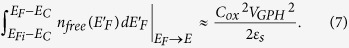
We have now extracted all the values of ΔVTRIS and ΔVTRnon-IS. This is summarized in Fig. 6(a). Here, the difference between ΔVTRIS and ΔVTRnon-IS is the density of recombined D2+/0. As a key observation in Fig. 6(a), both values of ΔVTRIS and ΔVTRnon-IS become similar when VGPH > 11 V. This suggests that the dominant mechanism is now the electron trapping rather than oxygen defect filling, and retrieving the oxygen defect profile beyond VGPH = 11 V may lead to ambiquities. From that information in Fig. 6(a), the density of the ΔD2+/0, i.e. n(ΔD2+/0), can be retrieved with the following equation 5,8, 9, 10,
Figure 6.

(a) VT shift after illumination stress following application of a series of gate pulses (green line) in comparison with that of the non-illumination stress sample after applying the series of gate pulses (orange line). (b) Extracted DOS of the ionized oxygen defects (D2+/0) vs. energy from conduction band (E-EC). The inset: correspondence between E-EC and VGPH. (c) Reaction between hydrogen and lattice oxygen. Here, electrons are donated from hydrogen, which are eventually used to occupy oxygen interstitials. (d) Illustration of the ionized oxygen interstitials (IO(oct)0) after illumination stress, as a possible source of the PPC. (e) Depiction of a further reaction between unoccupied oxygen interstitials (IO(oct)0) and lattice oxygen (LO2−), which yields (LO-IO(split))2− where is anti-bonding states located within the conduction band.
 |
where εs is the permittivity of channel layer, Cox the gate-insulator capacitance, and kT the thermal energy at ambient temperature. In addition, the distribution of the D2+/0 can be shown as a function of energy. For this, the VGPH value needs to be translated to E-EC using the surface potential, resulting in the following numerical relation26,27,
 |
Here, the free carrier density nfree is numerically computed based on Fermi-Dirac statistics28. We assume that the ionized states below EF are fully occupied and those above EF are unoccupied. Solving Equation (7), the correspondence between E-EC and VGPH is given, as shown in the inset of Fig. 6(b). Based on this, we can now retrieve the density of states of the D2+/0 (i.e. N(D2+/0)) as a function of energy (E-EC), using the following equation,
 |
As shown in Fig. 6(b), it is found that the profile of the ionized oxygen defect states is distributed in the energy range from −1.25 eV to +0.07 eV (above the conduction band minima). This result is quite consistent with the results shown in Fig. 4(d). As for the nature of these ionized states (D2+/0) within the gap (−1.25 eV to 0 eV), we consider both unoccupied octahedral-like oxygen interstitials (IO(oct)0) and oxygen vacancies (VO2+) as labeled at the top in Fig. 6(b). These states are initially occupied by 2 electrons, thus IO(oct)2−, which can be donated by hydrogen (H2) forming OH− with lattice oxygen (LO2−), as illustrated in Fig. 6(c)29. These interactions can be summarized as,
 |
 |
Before illumination, these octahedral oxygen interstitials are fully occupied, thus IO(oct)0. However, under illumination, electrons can be excited from the IO(oct)2− states. This process yields neutral states (IO(oct)0)29,30,31. These unoccupied states can remain unoccupied even after removal of illumination, thus it can be a possible form of the D2+/0 (see Fig. 6(d)).
As another possible form of the D2+/0 related to IO(oct)0, anti-bonding states of (LO-IO(split))2- are considered. This split oxygen interstitials (IO(split)) are derived from the interaction between IO(oct)0 and lattice oxygen (LO2−)25. This forms anti-bonding states within the conduction band, providing two free electrons. This results in PPC. In our experimental results shown in Fig. 6(b), the states within conduction band from 0 to 0.07 eV can be thought of as these anti-bonding states (σ*), i.e. (LO-IO(split))2−, between lattice oxygen (LO2−) and unoccupied octahedral oxygen interstitial (IO(oct)0)25 (see Fig. 6(e)).
Conclusions
Experimental evidence suggests that the negative threshold voltage shift under illumination stress and its post-stress persistency is due to metastable oxygen defect (vacancy and/or interstitial) ionization as opposed to carrier trapping/detrapping. Indeed, the inverse Laplace transform of transient recovery behavior post illumination stress as compared to that obtained under illumination stress yields activation energy distributions for two independent types of defect states; one that resides at a significantly higher activation energy level compared to the other. Here, the higher activation energy states limit the recovery rate after illumination stress, thus giving rise to persistent photoconductivity. The arguments are further corroborated by findings from gate pulse spectroscopy, which yields the post stress oxygen defect profile and also presence of anti-bonding states between lattice and interstitial oxygen atoms in the conduction band.
Additional Information
How to cite this article: Lee, S. et al. Oxygen Defect-Induced Metastability in Oxide Semiconductors Probed by Gate Pulse Spectroscopy. Sci. Rep. 5, 14902; doi: 10.1038/srep14902 (2015).
Supplementary Material
Acknowledgments
Authors thank to the EU-FP7 under Project ORAMA CP-IP 246334-2. Also, they would like to thank Dr. J. W. Jin, University of Cambridge, UK for technical discussions.
Footnotes
Author Contributions S.L. and A.N. designed the experiments. S.L. carried out the experiments, and S.L. and A.N. performed the analysis. S.J. fabricated the samples. All the authors contributed to discuss about the paper. S.L., A.N. and J.R. wrote the paper.
References
- Nomura K. et al. Room-temperature fabrication of transparent flexible thin-film transistors using amorphous oxide semiconductors. Nature 432, 488–492 (2004). [DOI] [PubMed] [Google Scholar]
- Nathan A. et al. Flexible electronics: the next ubiquitous platform. Proceedings of the IEEE 100, 1486–1517 (2012). [Google Scholar]
- Wager J. F., Keszler D. A. & Presley R. E. Transparent Electronics 1st edn (Springer, 2008). [Google Scholar]
- Robertson J. Disorder and instability processes in amorphous conducting oxides. Phys. Status Solidi B. 245, 1026 (2008). [Google Scholar]
- Jeon S. et al. Gated three-terminal device architecture to eliminate persistent photoconductivity in oxide semiconductor photosensor arrays. Nature Material 11, 301–305 (2012). [DOI] [PubMed] [Google Scholar]
- Liu J. S. et al. High responsivity ultraviolet photodetector realized via a carrier-trapping process. Appl. Phys. Lett. 97, 251102 (2010). [Google Scholar]
- Soci C. et al. ZnO Nanowire UV Photodetectors with High Internal Gain. Nano Lett. 7, 1003 (2007). [DOI] [PubMed] [Google Scholar]
- Nathan A. et al. Transparent Oxide Semiconductors for Advanced Display Applications, SID Info. Disp. Maga. 1, 6–11 (2013). [Google Scholar]
- Nathan A. et al. Amorphous Oxide Semiconductor TFTs for Displays and Imaging. J. Disp. Tech. 10, 917–927 (2014). [Google Scholar]
- Lee S. et al. Transparent Semiconducting Oxide Technology for Touch Free Interactive Flexible Displays. Proceedings of the IEEE 103, 4 (2015). [Google Scholar]
- Janotti A. & Van de Walle C. G. Oxygen vacancies in ZnO. Appl. Phys. Lett. 87, 122102 (2005). [Google Scholar]
- Lany S. & Zunger A. Anion vacancies as a source of persistent photoconductivity in II-VI and chalcopyrite semiconductors. Phys. Revi. B. 72, 035215 (2005). [Google Scholar]
- Oba F. et al. Defect energetics in ZnO: A hybrid Hartree-Fock density functional study, Phys. Revi. B 77, 245202 (2008). [Google Scholar]
- Agoston P., Albe K., Nieminen R. M. & Puska M. J. Intrinsic n-type behavior in transparent conducting oxides: A comparative hybrid-functional study of In2O3, SnO2, and ZnO, Phys. Revi. Lett. 103, 245501 (2009). [DOI] [PubMed] [Google Scholar]
- Clark S. J., Robertson J., Lany S. & Zunger A. Intrinsic defects in ZnO calculated by screened exchange and hybrid density functional. Phys. Revi. B 81, 115311 (2010). [Google Scholar]
- Fung T. C., Abe K., Kumomi H. & Kanicki J. Electrical Instability of RF Sputter Amorphous In-Ga-Zn-O Thin-Film Transistors. J. Disp. Tech. 5, 452 (2009). [Google Scholar]
- Wright S. W. & Anderson J. C. Trapping centres in sputtered SiO2 films. Thin Solid Films 62, 89 (1979). [Google Scholar]
- Chaji R. & Nathan A. Thin Film Transistor Circuits and Systems 1st edn (Cambridge University Press, 2013). [Google Scholar]
- Fomani A. A. & Nathan A. Metastability mechanisms in thin film transistors quantitatively resolved using post-stress relaxation of threshold voltage. J. Appl. Phys. 109, 084521 (2011). [Google Scholar]
- Luo J. et al. Transient photoresponse in amorphous In-Ga-Zn-O thin films under stretched exponential analysis. J. Appl. Phys. 113, 153709 (2013). [Google Scholar]
- Wager J. F., Yeh B., Hoffman R. L. & Keszler D. A. An amorphous oxide semiconductor thin-film transistor route to oxide electronics. Current Opinion in Solid State and Materials Science 18, 53 (2014). [Google Scholar]
- Studenikin S. A., Golego N. & Cocivera M. Optical and electrical properties of undoped ZnO films grown by spray pyrolysis of zinc nitrate solution. J. Appl. Phys. 83, 2104 (1998). [Google Scholar]
- Flewitt A. J. & Powell M. J. A thermalization energy analysis of the threshold voltage shift in amorphous indium gallium zinc oxide thin film transistors under simultaneous negative gate bias and illumination. J. Appl. Phys. 115, 134501 (2014). [Google Scholar]
- Saito R. & Murayama K. A universal distribution function of relaxation in amorphous materials. Solid State Comm. 63, 625 (1987). [Google Scholar]
- Robertson J. & Guo Y. Light induced instability mechanism in amorphous InGaZn oxide semiconductors. Appl. Phys. Lett. 104, 162102 (2014). [Google Scholar]
- Lee S. et al. Analytical Field-Effect Method for Extraction of Subgap States in Thin-Film Transistors. IEEE Elec. Devi. Lett. 33, 1006 (2012). [Google Scholar]
- Lee S. & Nathan A. Localized tail state distribution in amorphous oxide transistors deduced from low temperature measurements. Appl. Phys. Lett. 101, 113502 (2012). [Google Scholar]
- Lee S. et al. Trap-limited and percolation conduction mechanisms in amorphous oxide semiconductor thin film transistors. App. Phys. Lett. 98, 203508 (2011). [Google Scholar]
- Nomura K., Kamiya T. T. & Hosono H. Effects of Diffusion of Hydrogen and Oxygen on Electrical Properties of Amorphous Oxide Semiconductor, In-Ga-Zn-O. ECS J. Solid State Science and Technology 2, 5 (2013). [Google Scholar]
- Omura H. et al. First-principles study of native point defects in crystalline indium gallium zinc oxide. J. Appl. Phys. 105, 093712 (2009). [Google Scholar]
- Fung T. C. et al. Two-dimensional numerical simulation of radio frequency sputter amorphous In-Ga-Zn-O thin-film transistors. J. Appl. Phys. 106, 084511 (2009). [Google Scholar]
Associated Data
This section collects any data citations, data availability statements, or supplementary materials included in this article.