

Abstract
Polymer pen lithography (PPL) is a recently developed molecular printing technique which can produce features with diameters ranging from 80 nm to >10 μm in a single writing step using massively parallel (>107 pens) arrays of pyramidal, elastomeric pens. Leveling these pen arrays with respect to the surface to produce uniform features over large areas remains a considerable challenge. Here, we describe a new method for leveling the pen arrays that utilizes the force between the pen arrays and the surface to achieve leveling with a tilt of less than 0.004°, thereby producing features that vary by only 50 nm over 1 cm.
Polymer pen lithography1 (PPL) is a molecular printing2 method that combines the advantages of microcontact printing3–6 (μCP) and dip-pen nanolithography7–9 (DPN) by using as many as 107 elastomeric tips10, 11 to create arbitrary patterns of molecules on surfaces. PPL differs from μCP in several important respects2 that enable its unique writing capabilities. (1) PPL is a scanning probe printing technique capable of producing arbitrary patterns rather than replicas of the mold into which the stamp is poured, (2) As a result of the piezo-controlled movement of the pen array in the x- and y-direction, PPL can achieve nanometer scale registration between different features, whereas the mechanical properties of the stamps limit the separation of features and feature sizes that can be produced by μCP.12 (3) In PPL features with edge lengths ranging from 80 nm to over 10 μm can be patterned by the same pen by simply varying the dwell time of the tip on the surface or the force with which the pen is pressed onto the surface. The observation that edge lengths of features created by pyramidal arrays of PDMS were a function of contact force was first made in the context of a μCP experiment.6 However, there are major challenges in transitioning a contact printing tool based upon pyramidal arrays from the micro- or macroscale to the nanoscale, including tip-substrate alignment, ink diffusion control, lateral control over feature spacing, and feature size control. Some of these challenges have been overcome by attaching these tip arrays to piezoelectric actuators in the context of a PPL experiment.1 Indeed, with the current state of PPL, a digitized pattern can be printed with sub-100 nm control over feature diameter and position. Because the elastomeric pens are not damaged during writing, a pen array can be reused repeatedly, and the material cost for preparing a pen array is less than one US dollar. PPL has been utilized to fabricate circuit patterns,1 print multiplexed nanoarrays,13 and deposit nanomaterials14 over cm2 areas with nanometer scale registration and position control. While PPL maintains time-dependent ink transport15–18 – a characteristic of other tip-based, direct write molecular printing technologies, such as DPN – much of the utility of PPL arises from its unique force-dependent ink transfer mechanism.6, 19 As force is applied to the pyramidal elastomeric tips, they deform and the contact area between the tips and the surface increases, thereby producing larger features. By placing a scale beneath the substrate surface, we were able to measure the force generated between the pen array and the surface during writing and in turn derive a quantitative relationship that relates this force to the dimensions of the resulting features.19
A challenge that remains for researchers working with PPL involves finding a method to obtain precise leveling between the tip array and the substrate surface. When a tilting between these two planes exists, pens across the array will not contact the surface simultaneously, thereby producing patterns with different feature dimensions across the surface, especially when large pen arrays are used. The inability to produce uniform features over large areas presently limits the applicability of this technique to patterning small areas rather than full wafers. Currently, the plane of the PPL tip-array and the surface are leveled by bringing the tips into contact with the surface, and the deformation of the tips is observed by optical microscopy. The motors holding the pen array are subsequently adjusted until all tips appear to undergo an equivalent deformation upon contact with the surface. However, this optical method of leveling is not ideal, and features produced by widely separated pens have different edge lengths because of misalignment not identified by optical leveling and amplified over large distances. Our previous work has shown that the best optical leveling techniques cannot resolve less than a 0.02° difference in angle between the planes defined by the tip array and the substrate, respectively. This imprecision results in significant variations in feature edge length. For example, for an array of features with an average edge length of 3.83 μm, the outer most features, which are separated by 1 cm, exhibit a edge length difference of 1.73 μm.19 Also, optical leveling requires transparent pen arrays, and thereby limits array architecture and the materials that can be used to fabricate them.
Herein, we describe a new approach to level a pen array with respect to a substrate using force rather than optical methods. This method relies on our previously derived relationship between z-piezo extension and force and requires only a scale placed beneath the substrate to level the two planes.19 Although our current setup is limited to 0.004° tilt increments, this novel “force-feedback” method can theoretically achieve leveling to 1.6 × 10⁻⁴ °, when a scale with a sensitivity of 0.1 mN is used. This “force-feedback” leveling scheme will be described by first considering the force generated between the tips and the surface as the z-piezo holding the tip array is extended. Assuming perfect leveling, we have shown that the force, F, measured by a scale beneath the substrate is linearly related to the change in height of the polymer pen, Z, which, under perfect leveling, is also equal to the z-piezo extension, Z0 (Eq. 1):19
| (1) |
where N is the total number of polymer pens in the array, E is the compression modulus of the elastomer used (poly(dimethysiloxane (PDMS)) and H, Lbottom, and Ltop are the total height and edge lengths of the bottom and top surfaces of the pyramid prior to compression, respectively (Figure 1a). Moreover, it has been demonstrated previously that the E of PDMS depends on the compression ratio, which is described by the Mooney-Rivlin equation.20 To simplify the analysis, a two stage model of E is employed such that there exists a threshold value of z-piezo extension, zt, below which, E=E1=1.38Mpa19 and above which, E=E2=8.97Mpa.21 This simplified, two-stage model (Eq. 2 and 3) fits the experimentally observed data for the force produced by the pen array on the surface, F, for different values of Z.19
Figure 1.
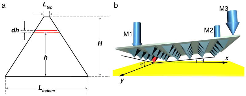
(a) Geometric model of the tip. (b) An unleveled polymer pen array with a tilt of θ° along the y-axis and a tilt of φ° along the x-axis is brought into contact with the surface. The red pen indicates the initial point of contact with the surface.
| (2) |
| (3) |
Considering the case when the leveling between the tip array and the surface is imperfect, the tilting can be described by two angles, θ and φ, that correspond to the tilting between the plane of the pen array and the substrate on the y and x axes, respectively (Figure 1b). When the z-piezo is extended, the compression of each pen, Z, varies as a function of θ and φ, and the distance of each pen from the closest pen to the surface. If the compression of the first pen to contact the surface is Z0, the Z for any single pen in the array can be calculated (Eq. 4):
| (4) |
where D is the spacing between pens, and Nx and Ny are the number of pens from the first pen to contact the surface along the x and y axes, respectively. The effect of an unleveled pen array (with respect to the surface) on the uniformity of the generated features can be significant. In the case of a tilt as small as (θ, φ) = (0.15°, 0.1°), pens only 5 mm away from the first pen to contact the surface will not come into contact with the surface (Figure 2), and therefore not write.
Figure 2.

The change in height for every individual pen in the polymer pen array with: (a) θ =0 and φ=0, and (b) θ =0.15° and φ=0.10°. Spacing between pens is 80 μm, and the z-piezo extension is 12 μm.
By substituting Eq. 5 into Eqs. 2 and 3, the force generated by any single pen on the surface can be calculated as a function of Z, θ, φ, Nx and Ny (Eq. 5 and 6).
| (5) |
| (6) |
Using Eq. 6, the total force, Ftotal, generated on the substrate by a tilted pen array, with a spacing D between pens, can be calculated as a function of θ and φ (Eq. 7).
| (7) |
Because Ftotal is a function of θ and φ, when these angles are changed, Ftotal between the PPL pen array and the surface also changes for the same z-piezo extension (Z0) (Figure 3). From this relationship, several conclusions can be drawn: (1) At (θ, φ) = (0, 0), which is the perfect leveling position, the total force between the tip array and the surface reaches its global maximum. (2) For any given value of θ, Ftotal reaches a local maximum value when φ=0, or vice versa. (3) As θ and φ approach 0, the gradient in force with respect to changes in angle, ∂F/∂θ and ∂F/∂φ, increases (Eqs.8 and 9), resulting in a high sensitivity to changes in θ and φ near the perfect leveling position. This model suggests that the force measured between the PPL pen array and the sample surface can indeed be used to level the two planes within 0.004° using a scale with a sensitivity of 0.1 mN (Eqs. 8 and 9).
Figure 3.

Total force (Ftotal) between the polymer pen array and the surface plotted as a function of θ and φ according to Eq. 7. The parameters for this plot are N=10000 pens, Z0= 12 μm and Ltop ,=70 nm. 19
| (8) |
| (9) |
where E = E1 for tips when Z < zt and E = E2 for tips when Z > zt.
This new relation between the detected force and the degree of tilt between the tip array and the sample surface (Eq. 7) was tested by adjusting θ and φ, measuring the force as the z-piezo is extended, writing with the pen array, and comparing the features produced at different forces by a PPL pen array. To perform these experiments, a 1 cm2, ~10000-pen polymer pen array with D = 80 μm was mounted onto an NScriptor (NanoInk, Inc) nanolithography platform, and the pens were inked with 16-mercaptohexadecanoic acid (MHA), which can form a self-assembled monolayer (SAM) on a Au surface. A 25 nm thermally evaporated Au thin film with 5 nm Ti adhesive layer on a Si<100>/SiOx substrate was mounted on a scale (Ohaus, PS121) with a sensitivity of 0.1 mN. The pen array was brought into contact with the surface until a force of 1 mN was detected, and then the z-piezo was extended to Z0 =12 μm, and the force was recorded. θ and φ were changed by systematically adjusting the three motors holding the pen array, M1, M2, and M3 (Figure 1b). When M1 and M3 are fixed and M2 increases by 100 μm, φ will increase 0.08°. When M2 and M3 are fixed and M1 increases by 100 μm, θ will increase 0.04°. To find a local maximum of Ftotal, one angle is held constant, while the other is varied. This maximum is either the θ or φ ~ 0° point. This suggests a systematic leveling strategy: first, θ is fixed and φ is varied until a local maximum of Ftotal is found φ ~ 0°. Then φ is fixed at the optimized value and θ is searched for the local maximum of Ftotal. Finally, θ and φ are finely varied near the second local maximum until a global maximum of Ftotal is found, i.e. (θ, φ) = (0, 0). After patterning at different values of θ and φ, the patterned substrate was placed in a Au etching solution (20 mM thiourea, 30 mM FeNO2, 20 mM HCl and 20 mM octanol (aq)) 1, leaving Au only where the MHA had been deposited by the PPL pen array. The gold patterns were subsequently characterized by scanning electron microscopy (SEM).
The iterative approach to leveling was tested by mounting the PPL pen array onto the NScriptor and maximizing Ftotal between the pens and the surface upon adjusting θ and φ. In this experiment, the pens were brought into contact with the surface by extending the z-piezo, and the force was subsequently measured. Initially, θ was held constant and φ was systematically adjusted, and Ftotal was measured upon a Z0 of 12 μm, until the local maximum Ftotal was found. This local maximum occurred at ainchange of ~0.7° from the initial tilt of the pen array, and corresponded to a change in Ftotal of approximately 10 mN, a value well within the sensitivity of the scale (Figure 4a). The second local maximum was found by holding φ constant and varying θ, which occurred at a change in θ of ~0.65° and a change in force of ~25 mN (Figure 4b). It should be noted that the increase in force for the second local maximum compared to the first local maximum − 25 mN compared to 10 mN for a nearly identical change in angle – is in agreement with the theoretical model that predicts a steeper gradient as leveling approaches (θ, φ) = (0, 0). Finally a global maximum in Ftotal was found by making minute changes in θ, where a change in 0.06° resulted in a change in Ftotal of ~7 mN (Figure 4c). The superimposition of the three leveling curves (Figure 4d) matches well with the shape of the model for Ftotal (θ, φ) (Figure 3). However, the measured values of Ftotal do not agree exactly with the predicted values because the scale produces imprecise readings as a result of strain on the scale by a tilted pen array.
Figure 4.

Three-step leveling strategy for PPL. a) To level the pen array with respect to the surface, initially, θ is held constant and φ is varied until a local maximum in Ftotal is found. b) Subsequently θ is varied, and φ is held constant until another local maximum in Ftotal is found. c) Finally, θ is held constant and φ is varied again until a global maximum in Ftotal is found. d) By combining the plots (a–c), a 3-D plot is constructed that shows that the experimentally determined relation between the force measured by the scale beneath the substrate as a function of θ and φ agrees with the theoretically predicted curve (Figure 3).
Finally, patterns of MHA on Au were written at different values of Ftotal by adjusting θ and φ from the perfect leveling position, and the pattern uniformity by different pens across the array was measured. Initially, the pens were leveled according to the procedure described above to a Ftotal value of 36.0 mN, and MHA dots were written by extending the z-piezo 10 μm, resulting in patterns where a single dot was written by each pen in the array (Figure 5a). The motors were adjusted to a value of (θ, φ) = (0.01, 0), which corresponded to a Ftotal of 33.6 mN, and an identical pattern of MHA dots was written (Figure 5b). Finally, the motors were adjusted to a value of (θ, φ) = (−0.01, 0), which corresponded to a Ftotal of 35.0 mN, and a pattern of MHA dots was written (Figure 5c). The Au was etched from areas where the MHA had not been deposited, and the resulting Au features were imaged by SEM. The plot of the variance of the feature edge length as a function of distance from one side of the pen array for the three different curves demonstrates that patterns written at the maximum Ftotal are the most uniform (Figure 5d). For the patterns written at the highest Ftotal, average edge length was 2.54 ± 0.05 μm, which corresponds to approximatedly 2% variation from the average value. This feature size distribution is similar to that produced in single tip DPN experiments, which may be caused by small differences in pyramid shape and inhomogeneous inking of different pens. For the patterns written at (θ, φ) = (0.01, 0) or (−0.01, 0), the average feature edge lengths are 4.68 μm ± 0.89 μm and 5.33 ± 1.03 μm, respectively. Importantly, for the patterns printed at a defined tilt, the error is not random, rather feature diameters either increase or decrease according to the angle of tilt between the pen array and the surface, which is often the case when the pens are leveled by optical methods.19
Figure 5.

The patterns made by a 10,000 pen array with (a) θ = 0, (b) θ = 0.01, and (c) θ= −0.01 °, respectively. Scale bar is 50 μm. (d) The relation between feature size and the distance to one side of the polymer pen array under different leveling conditions. (e) The diameters of different features plotted as a function of distance from one side of the pen array at different values of θ.
In conclusion, we have mathematically described the relationship between the force between a PPL pen array and the surface and the tilting between these two planes. This relation can be used to level the two planes to 0.004° and results in features that vary in diameter by only 50 nm over a distance of 1 cm. In addition, this method does not require a transparent pen array and lends itself to automation. This work is an important step towards attaining the goal of a “desktop fab,” in which reproducible, nanoscale patterns can be printed over large areas without necessitating large capital investment or clean-room conditions.
Experimental
Preparation and characterization of dot arrays
Polymer pen arrays with 10,000 pens and 80 μm separation between tips were prepared, and the pen arrays were inked with 16-mercaptohexadecanoic acid (MHA) as previously described.1 The polymer pen arrays were mounted onto an NScriptor (NanoInk, Inc., USA) nanolithographyl platform for all patterning experiments. Au nanostructures were prepared by patterning the MHA on 25 nm thick, thermally evaporated Au films with a 5 nm Ti adhesion layer thermally evaporated on Si<100>/SiOx wafers (Nova Electronic Materials, USA). The tip position, z-piezo extension dwell-time between the inked tip arrays and the Au surfaces, and humidity were controlled by InkCAD (NanoInk, Inc., USA) software. Upon immersion of the patterned surface in an etching solution (20 mM thiourea, 30 mM FeNO2, 20 mM HCl and 20 mM octanol (aq)) for approximately 5 min, the Au was dissolved selectively from areas that are not capped by the MHA. The resulting Au features were analyzed by scanning-electron microscopy (SEM Hitachi S-4800, Japan) and a Zeiss Axiovert 200M (Carl Zeiss, Inc., Germany) optical microscope.
“Force-Feedback” leveling
A scale (PS121, Ohaus, USA) was placed beneath the substrate to be patterned. The MHA-inked tip arrays were brought into contact with the surface so that deformation of the pyramids could be observed optically, but no force was detected by the scale. This point was set at z-piezo extension = 0 μm. θ and φ were changed by systematically adjusting the three motors holding the pen array, M1, M2, and M3. When M1 and M3 are fixed and M2 increases by 100 μm, φ will increase 0.08°. When M2 and M3 are fixed and M1 increases by 100 μm, θ will increase 0.04°. To find a local maximum of Ftotal, one angle is held constant, while the other is varied. This maximum is either the θ or φ ~ 0° point. First, θ is fixed and φ is varied until a local maximum of Ftotal is found φ ~ 0°. Then φ is fixed at the optimized value and θ is searched for the local maximum of Ftotal. Finally, θ and φ are finely varied near the second local maximum until a global maximum of Ftotal is found, i.e. (θ, φ) = (0, 0).
Acknowledgments
CAM acknowledges DARPA-SPAWAR, the AFOSR, and the NSF-NSEC. ABB is grateful to the NIH for financial support (5F32CA136148-02).
References
- 1.Huo FW, Zheng ZJ, Zheng GF, Giam LR, Zhang H, Mirkin CA. Science. 2008;321:1658–1660. doi: 10.1126/science.1162193. [DOI] [PMC free article] [PubMed] [Google Scholar]
- 2.Braunschweig AB, Huo FW, Mirkin CA. Nat Chem. 2009;1:353–358. doi: 10.1038/nchem.258. [DOI] [PMC free article] [PubMed] [Google Scholar]
- 3.Kumar A, Whitesides GM. Appl Phys Lett. 1993;6:2002–2004.3. [Google Scholar]
- 4.Xia YN, Rogers JA, Paul KE, Whitesides GM. Chem Rev. 1999;9:1823–1848.9. doi: 10.1021/cr980002q. [DOI] [PubMed] [Google Scholar]
- 5.Xia YN, Whitesides GM. Adv Mater. 1995;7:471–473. [Google Scholar]
- 6.Wilbur JL, Kim E, Xin YN, Whitesides GM. Adv Mater. 1995;7:649–652. [Google Scholar]
- 7.Piner RD, Zhu J, Xu F, Hong SH, Mirkin CA. Science. 1999;283:661–663. doi: 10.1126/science.283.5402.661. [DOI] [PubMed] [Google Scholar]
- 8.Ginger DS, Zhang H, Mirkin CA. Angew Chem Int Ed. 2004;4:30–45.3. [Google Scholar]
- 9.Salaita K, Wang YH, Mirkin CA. Nat Nanotech. 2007;2:145–155. doi: 10.1038/nnano.2007.39. [DOI] [PubMed] [Google Scholar]
- 10.Hong JM, Ozkeskin FM, Zou J. J Micromech Microeng. 2008;1:015003.8. [Google Scholar]
- 11.Qin D, Xia YN, Black AJ, Whitesides GM. J Vac Sci Tech B. 1998;1:98–103.6. [Google Scholar]
- 12.Zheng Z, Jang JW, Zheng G, Mirkin CA. Angew Chem Int Ed. 2008;4:9951–9954.7. doi: 10.1002/anie.200803834. [DOI] [PMC free article] [PubMed] [Google Scholar]
- 13.Zheng Z, Daniel WL, Giam LR, Huo F, Senesi AJ, Zheng G, Mirkin CA. Angew Chem Int Ed. 2009;4:7626–7629.8. doi: 10.1002/anie.200902649. [DOI] [PMC free article] [PubMed] [Google Scholar]
- 14.Huang L, Braunschweig AB, Shim W, Qin L, Hurst SJ, Huo F, Xue C, Jang J-W, Mirkin CA. Small. 2009 doi: 10.1002/smll.20091198. [DOI] [PMC free article] [PubMed] [Google Scholar]
- 15.Jang JY, Hong SH, Schatz GC, Ratner MA. J Chem Phys. 2001;115:2721–2729. [Google Scholar]
- 16.Manandhar P, Jang J, Schatz GC, Ratner MA, Hong S. Phys Rev Lett. 2003;9:115505. doi: 10.1103/PhysRevLett.90.115505. [DOI] [PubMed] [Google Scholar]
- 17.Weeks BL, Noy A, Miller AE, De Yoreo JJ. Phys Rev Lett. 2002;8:255505.8. doi: 10.1103/PhysRevLett.88.255505. [DOI] [PubMed] [Google Scholar]
- 18.Giam LR, Wang YH, Mirkin CA. J Phys Chem A. 2009;113:3779–3782. doi: 10.1021/jp809061e. [DOI] [PubMed] [Google Scholar]
- 19.Liao X, Braunschweig AB, Mirkin CA. Small. 2009 doi: 10.1002/smll.200901538. [DOI] [Google Scholar]
- 20.Mark J. Physical Properties of Polymers Handbook. 2. Springer; New York: 2006. [Google Scholar]
- 21.Schmid H, Michel B. Macromolecules. 2000;3:3042–3049. [Google Scholar]