Abstract
Silicon-based photonics is now considered as the photonic platform for the next generation of on-chip communications. However, the development of compact and low power consumption optical modulators is still challenging. Here we report a giant electro-optic effect in Ge/SiGe coupled quantum wells. This promising effect is based on an anomalous quantum-confined Stark effect due to the separate confinement of electrons and holes in the Ge/SiGe coupled quantum wells. This phenomenon can be exploited to strongly enhance optical modulator performance with respect to the standard approaches developed so far in silicon photonics. We have measured a refractive index variation up to 2.3 × 10⁻³ under a bias voltage of 1.5 V, with an associated modulation efficiency VπLπ of 0.046 V cm. This demonstration paves the way for the development of efficient and high-speed phase modulators based on the Ge/SiGe material system.
Silicon photonics has generated strong advances in recent years for on-chip optical communications. Silicon based-optoelectronic devices have been intensively studied and the recent advances proved the capability of silicon photonics to offer some viable solutions for many applications including optical telecommunications and optical interconnects. In this context Ge rich-Ge/SiGe quantum wells (QW) have received a growing interest since the first demonstration of the quantum-confined Stark effect (QCSE) in these structures in 20051. The QCSE causes a red-shift of the absorption spectrum and a significant reduction of the excitonic absorption peak2; features that can be exploited for optical intensity modulation. This result paved the way to a number of exciting works addressing the absorption mechanisms in Ge/SiGe QW structures and tackling the fabrication of innovative optoelectronic devices in the near-IR wavelength range (1.3 μm-1.5 μm). Compact and efficient intensity modulators at wavelengths of 1490 nm3,4,5,6 and 1550 nm7,8 have been demonstrated as well as high-speed behaviour9. The most striking feature of electro-absorption modulators based on the QCSE is the possibility to reach power consumption lower than 100 fJ/bit, as demonstrated in9, thus meeting the aggressive requirements for on-chip optical interconnects10. As a major advantage, the compositions and thicknesses of the layers in a Ge/SiGe QW can be engineered to modify the electro-optical properties, such as to address modulation at 1.3 μm wavelength11,12,13. All the aforementioned modulators works by exploiting electroabsorption based on the QCSE of excitonic transitions between the first valence band heavy hole or light hole level (HH1 or LH1), and the first conduction state at Γ (cΓ1). In contrast, much less research effort has been spent on investigating the change in Ge/SiGe QW refractive index due to the variations of their absorption spectra, i.e. electrorefraction, as given by the Kramers-Kronig relations. Indeed only recently, an experimental value of effective refractive index variation of 1.3 × 10⁻³ under −8 V, with a figure merit VπLπ of 0.46 Vcm was reported for Ge/Si0.15Ge0.85 QW14. In this preliminary demonstration, the voltage required to induce electro-refraction effect was too high to be compatible with the voltage delivered by CMOS microelectronic circuits. However, the electro-optical properties of quantum well structures can be further tailored by coupling quantum wells together. Coupled quantum wells (CQW) exhibit interesting physical behaviours due to the coupling of the wave-functions through the barrier, allowing an ultimate control of the electro-optical properties. For this reason, in III-V semiconductors, symmetric and asymmetric CQW have been widely investigated for many purposes including non-linear optics15, infrared photodetection16, THz emission17 and low-voltage optical modulation18. Theoretically, symmetrically Ge/SiGe CQW have been proposed to enhance the electro-refractive effect19. A surfaced-illuminated Ge CQW device was recently fabricated20; in this case the electro-absorption was studied through resistivity measurements. In this work we report the first experimental demonstration of Ge/SiGe CQW waveguide showing an anomalous QCSE and a strong electro-refraction effect under low bias voltage. The electro-optical properties of Ge/SiGe CQWs have been experimentally investigated by means of optical transmission measurements of a Fabry Perot cavity. The absorption spectra analysis and the comparison with theoretical modelling shows the influence of the coupling of the quantum wells and the necessity to consider the two first electron and heavy hole confined states to understand the experimental features. Electro-refraction is deduced from the Fabry Perot resonance shifts as a function of the applied electrical field. The results have been used to evaluate the characteristics of a phase-shifter based on this structure.
Results
Device design
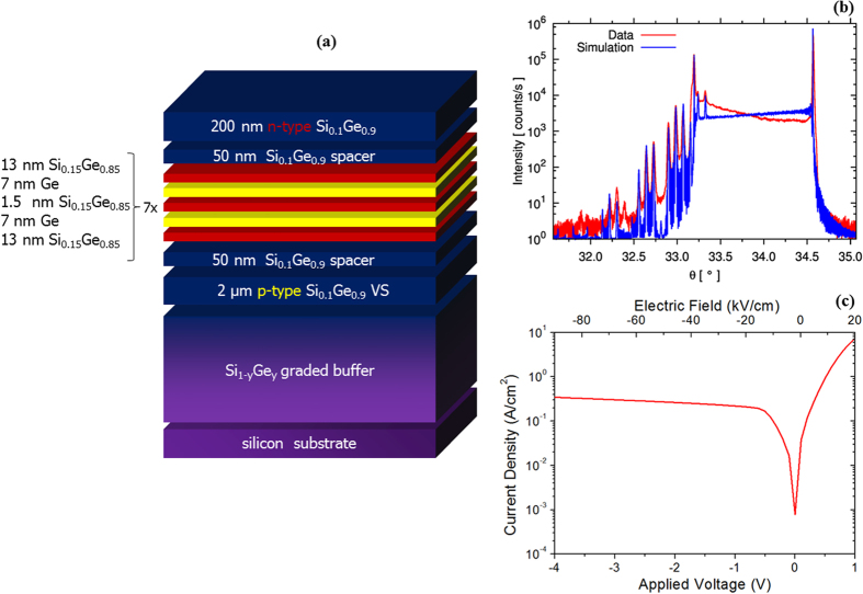
The CQW heterostructure was grown by low-energy plasma-enhanced chemical vapour deposition (LEPECVD)21. A cross section of the structure is shown in Fig. 1(a). The CQW consists of seven pairs of CQWs: 7 × [7 nm Ge QW + 1.5 nm Si0.15Ge0.85 inner barrier + 7 nm Ge QW + 26 nm Si0.15Ge0.85 outer barrier]. Individual layer thicknesses and compositions were designed to obtain a strain-symmetrized structure. The outer barrier is thick enough to avoid coupling between adjacent periods. The symmetric ω-2θ scan (taken through the Si(004) Bragg peak) is reported in Fig. 1(b). The good agreement between the experimental and the dynamically simulated X-ray diffraction spectra confirms the presence of the thin Si0.15Ge0.85 inner barrier. The CQW are embedded in a PIN diode in order to apply an electrical field perpendicular to the CQW planes. In Fig. 1(c) is reported the current density as a function of the applied voltage and of the electric field.
Figure 1.
(a) Cross section of the sample showing the Ge/SiGe CQW between n-doped SiGe and p-doped SiGe to form a PIN diode. The stack is grown on a Si substrate via a graded buffer by LEPECVD. (b) X-ray diffraction: the agreement between experimental and simulated ω-2θ scans around the(004) reflection confirms that the CQW structure has been realized. (c) Current density of the device as a function of the applied voltage.
Electro-Refraction measurement in CQW
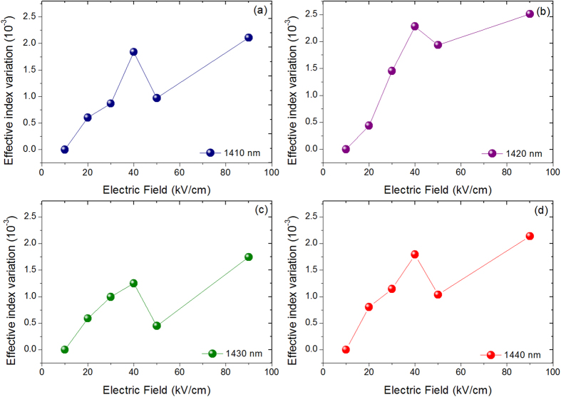
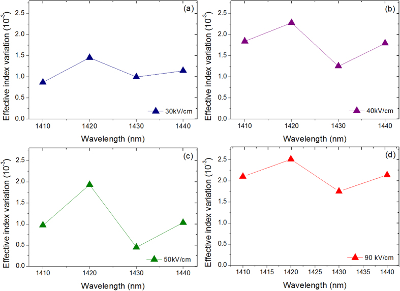
64 μm long planar waveguide has been fabricated to investigate the electrorefraction in Ge/SiGe CQW. At wavelengths larger than the absorption band-edge (located around 1400 nm), Fabry Perot fringes induced by multiple reflections at the waveguide facets have been analyzed. As an example, a Fabry Perot fringe around 1422 nm and its shift as a function of the electrical field is reported in Fig. 2. The effective index variation was experimentally deduced at different wavelengths, using the method described in ref. 14. The measured effective index variation as a function of the electric field is reported in Fig. 3 for different wavelengths above the absorption band-edge. Due to the built-in potential, an electric field of 10 kV/cm is present when the applied bias voltage is 0 V. Strikingly, the refractive index variation shows a local maximum at an electric field of 40 kV/cm for all considered wavelengths. Conversely, in a standard non-coupled quantum well the effective index increased quadratically with the electrical field14. Interestingly, the effective index variation also shows a maximum at a wavelength of 1420 nm for all the considered electric fields (see Fig. 4), while in standard QW it continuously decrease as the wavelength increases14. As a consequence, CQW structures can be specially tailored for optimized operation at low-bias for different spectral region. In the following section, the absorption spectra of Ge/SiGe CQW have been measured and theoretically analyzed to explain the anomalous behavior of the effective index variation with the applied electric field and as a function of the wavelength.
Figure 2. Electro-refraction measurement.
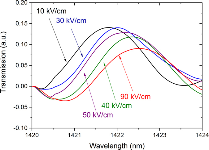
The wavelength dependence of the transmission is characteristic to the Fabry Perot effect induced by multiple reflections at the waveguide facets.The shift of the fringes with the applied electric field is related to the refractive index variation in the CQW structure.
Figure 3.
Effective index variation as a function of the electric field at 1410 nm (a), 1420 nm (b), 1430 nm (c) and 1440 nm (d).
Figure 4.
Effective index variation as a function of the wavelength at 30 kV/cm (a), 40 kV/cm (b), 50 kV/cm (c) and 90 kV/cm (d).
Absorption spectra analysis
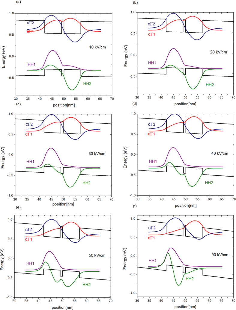
The absorption spectra of the device at different reverse bias voltages obtained from optical transmission measurements are reported in Fig. 5 for TE polarization. The data have been filtered and the baseline of each curve has been shifted by 200 cm−1 to better highlight the spectral features. From these measurements the absorption spectra in Ge/SiGe CQW show unique characteristics which differ from those previously recorded in standard non-coupled Ge/SiGe QW14. A combination of increasing/decreasing absorption peaks is obtained when the electrical field varies from 10 kV/cm to 90 kV/cm. To understand this behavior, the measurements are compared with simulations performed within the envelope function approximation using the Nextnano software package22. The simulated wavefunctions of cΓ1, cΓ2, HH1 and HH2 in the CQW as a function of the applied electric field are reported in Fig. 6. In a CQW, the cΓ1 (resp. HH1) and cΓ2 (resp. HH2) transitions represents the “bonding” (zero-node wavefunction) and “anti-bonding” (one-node wavefunction) which are formed due to the QW coupling. In such a system, the electric field breaks the symmetry, thus the optical transitions HH2-cΓ1 and HH1-cΓ2 are no longer forbidden by selection rules as in standard uncoupled quantum wells and consequently the absorption spectra, in the considered energy range, consist of a combination of four optical transition: HH1-cΓ1 (T11), HH2-cΓ2 (T22), HH2-cΓ1 (T12) and HH1-cΓ2 (T21). At 10 kV/cm the cΓ1 and cΓ2 wavefunctions are still delocalized on both wells, while the HH1 and HH2 wavefunctions show a significative localization in the left and right wells respectively (see Fig. 6a). The absorption spectrum at 10 kV/cm is dominated by two spectral features: a peak located at 0.909 eV and a shoulder at lower energy which are formed by a superposition between the T22 and T21 transitions and between the T11 and T12 transitions respectively. The simulations show that, as the field increases, the spatial overlap between the wavefunctions (and consequently the intensity of the associated optical transition) of T12 and T21 increases, while that of T11 and T22 decreases. Moreover, as the electric field increases, the T22 and T12 transitions red-shift while the T11 and T21 transitions are blue-shifting. As a consequence, a clear blue-shift of the high energy peak is observed in the absorption spectra recorded at 20 kV/cm and at 30 kV/cm. The intensity of the low energy spectral feature increases because there is an increasing spectral overlap between the T12 and T21 transitions. At 40 kV/cm the absorption spectrum is dominated by two peaks clearly recognizable at 0.912 eV and at 0.897 eV. The simulations show that the spatial overlap between the wavefunctions associated to the T11 and T22 become vanishingly small at 40 kV/cm, and consequently the two peaks have been attributed to the T21 and T12 transitions. As the electric field increases, the spectral overlap between the T21 and T12 transitions increases, and at 90 kV/cm, only a single broad peak is visible in the absorption spectrum. As a conclusion of this analysis, the unusual behavior of the QCSE in CQW is explained by the evolution of both electron and hole wavefunctions in the CQW as a function of the electric field. The number of excitonic transition and the strong evolution of the excitonic peak intensities near the absorption band-edge are quite different from the normal QCSE, which explains the large electrorefraction and its non-usual wavelength dependence measured in this structure.
Figure 5. Absorption spectra as a function of the applied electric field.
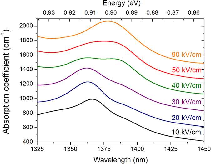
The data have been filtered and the baseline of each curve has been shifted of 200 cm−1.
Figure 6.
Simulated wavefunctions in the CQW at Γ point, of the cΓ1, cΓ2, HH1 and HH2 with an electric field of: (a) 10 kV/cm, (b) 20 kV/cm, (c) 30 kV/cm, (d) 40 kV/cm, (e) 50 kV/cm and (f) 90 kV/cm.
Discussion
The anomalous CQSE in the Ge/SiGe CQW structure leads to effective index variations of more than 2 × 10⁻³ under an electrical field of only 40 kV/cm. In comparison, in classical uncoupled Ge/SiGe QW structures an effective index variation of 1.3 × 10⁻³ was measured with an applied electric field of 88 kV/cm. Using the CQW structure, under a bias voltage as low as 1.5 V (corresponding to an electric field of 40 kV/cm) on a 300 μm-long structure is enough to obtain a π phase shift. A VπLπ figure of merit of only 0.046 V cm can then be deduced, which is one order of magnitude better than in uncoupled Ge/SiGe QWs14 and very competitive with respect to Si-based phase shifters23,24. In addition the VπLπ figure of merit can be further improved by increasing the overlap between the optical mode and the QW region (which was 17% in this work). Optimizing this overlap will also allow a reduction of the optical losses caused by the thick p-doped SiGe virtual substrate in this tested structure. To fully exploit the potentiality of Ge/SiGe CQW as compact, high speed and low power consumption optical modulators, the active region will have to be integrated into an interferometric structure such as a Mach– Zehnder interferometer. It can be noticed that the integration of QW active regions with low-loss SiGe waveguides on top of graded buffer is a promising approach, as the integration of a passive SiGe waveguide with an electro-absorption modulator and a modulator was demonstrated recently25. Remarkably, all the devices were monolithically integrated on silicon by a single epitaxial growth. Finally besides the interest for low power consumption optical modulators, the control of quantum confinement in Ge/SiGe CQW paves the way of a new route towards the exploitation of nonlinear optical effects in Ge/SiGe.
Methods
Epitaxial growth and characterization
The CQW heterostructure was grown by low-energy plasma-enhanced chemical vapor deposition (LEPECVD)21 on a 100 mm n-Si(001) substrate with a resistivity of 1–10 Ω cm. Before the heteroepitaxial growth, the substrate was dipped in an aqueous hydrofluoric acid solution for 30 seconds to remove the native oxide. The first part of the structure consists of a Si1-yGey graded buffer, with a total thickness of 13 μm, where the Ge concentration y was linearly raised from 0% to 90% with a grading rate of 7%/μm. The growth rate was 5–10 nm/s, while the substrate temperature was linearly decreased from 740 °C to 525 °C . The graded buffer was then capped with a 2 μm thick p-doped (5 × 1018 cm−3) Si0.1Ge0.9 layer to form a fully relaxed virtual substrate (VS) and the p-type contact of the p-i-n structure embedding the CQWs. The threading dislocation density was 6 × 106 cm−2 as measured by chemical defect etching26. The CQW consists of seven repetitions of the following period: 7 nm Ge well +1.5 nm Si0.15Ge0.85 inner barrier +7 nm Ge well +26 nm Si0.15Ge0.85 outer barrier. The CQW structure was grown at rate of 1 nm/s and the temperature was lowered at 475 °C to avoid the interdiffusion at the barrier/QW interfaces. Finally, a 200 nm phosphorous doped (1 × 1019 cm−3) Si0.1Ge0.9 n-type contact layer was deposited. Layer compositions and strain states were measured by high-resolution x-ray diffraction (HR-XRD) using a PANalytical X’Pert PRO MRD diffractometer. Out-of-plane and in-plane lattice parameters were measured (relative to the Si (004) reflection) for the VS peak and the superlattice satellites. Ge content and strain were then obtained using the known lattice parameters for relaxed SiGe alloys27 and interpolated elastic constants of Si and Ge28. The final composition of the VS was found to be 90% (with a residual in-plane strain of 0.12%). The in-plane lattice parameter of the CQW stack is the same as that of the VS, meaning that the CQW stack is coherently matched to the VS.
Device fabrication
The waveguides were patterned by dry etching to the p-doped Si0.1Ge0.9 layer. The sidewall roughness of the etched mesa was smoothened by hydrogen peroxide (H2O2) solution. 100 nm of silicon dioxide were deposited as passivation layer on the left and right walls of the waveguide by plasma-enhanced chemical vapor deposition (PECVD). For n and p contacts 10 nm of Ti and 300 nm of Au was evaporated and lifted off.
Optical transmission measurements
The measurements were performed at room temperature with spectral resolution of 0.1 nm. A tunable laser from 1325 to 1450 nm with an output power of 1 mW was used. Light from the laser was butt coupled into the waveguide using a lensed fiber. Light was injected into the waveguide part which was not covered by the metal to minimize optical losses. An objective was used to couple the output light into a photodetector. Light polarization was controlled at the input and the output of the waveguide. The transmission of the device is normalized by the transmission of the set-up to take into account its wavelength dependence. Calculations have been performed in order to investigate the effect of the air/waveguide reflection on the transmission spectra. A homogenized medium of Si0.1Ge0.9 is considered on top of the graded buffer, with a refractive index of 4.228 at 1.32 μm and 4.209 at 1.45 μm. Effective indexes of 4.222 and 4.202 are obtained at the wavelengths of 1.32 μm and 1.45 μm, respectively. A reflection of 38.07% is obtained at 1.32 μm and 37.89% at 1.45 μm. The corresponding losses difference is thus around 0.02 dB, thus the effect of the air/waveguide reflection on the the transmission spectra is negligible.
Additional Information
How to cite this article: Frigerio, J. et al. Giant electro-optic effect in Ge/SiGe coupled quantum wells. Sci. Rep. 5, 15398; doi: 10.1038/srep15398 (2015).
Acknowledgments
The CARIPLO foundation is acknowledged for financial support through the grant EIDOS 2011-038. The fabrication of the device was performed at the nano-center CTU-IEF-Minerve, which is partially funded by the ‘Conseil Général de l’Essonne’. This work was partly supported by the French RENATECH network. D.M-M. acknowledges support by the Institut Universitaire de France. Marie Curie International Outgoing Fellowships through grant agreement PIOF-GA-2013-629292 MIDEX is partly acknowledged. This project has received funding from the European Research Council (ERC) under the European Union’s Horizon 2020 research and innovation programme (grant agreement N°639107-INsPIRE).
Footnotes
The authors declare no competing financial interests.
Author Contributions J.F., G.I. and D.M.M. conceived the project. J.F. designated the sample structure, carried out epitaxial growth, simulations and data analysis. V.V., P.C. and M.F. designed and fabricated the devices and carried out optical measurements. D.C. performed XRD measurements and analysis. X.L.R., L.V., G.I. and D.M.M. supervised the project. All of the authors contributed to manuscript preparation.
References
- Kuo Y. H. et al. Strong quantum-confined stark effect in germanium quantum-well structures on silicon. Nature 437, 1334–1336 (2005). [DOI] [PubMed] [Google Scholar]
- Miller D. A. B. et al. Bandedge Electro-absorption in quantum well structures: the quantum confined stark effect. Phys. Rev. Lett. 53, 2173–2177 (1984). [Google Scholar]
- Chaisakul P. et al. Quantum-confined Stark effect measurements in Ge/SiGe quantum-well structures. Opt. Lett. 35, 2913–2915 (2010). [DOI] [PubMed] [Google Scholar]
- Chaisakul P. et al. Polarization dependence of quantum confined Stark effect in Ge/SiGe quantum well planar waveguide. Opt. Lett. 36, 1794–1796 (2011). [DOI] [PubMed] [Google Scholar]
- Ren S., Rong Y., Kamins T. I., Harris J. S. & Miller D. A. B. Selective epitaxial growth of Ge/Si0.15Ge0.85 quantum wells on Si substrate using reduced pressure chemical vapor deposition. Appl. Phys. Lett. 98, 151108 (2011). [Google Scholar]
- Ren S. et al. Ge/SiGe quantum well waveguide modulator monolithically integrated with SOI waveguides. IEEE Photon. Tech. Lett. 24, 461–463 (2012). [Google Scholar]
- Kuo Y. H. et al. Quantum-confined stark effect in Ge/SiGe quantum wells on Si for optical modulators. IEEE J. Sel. Top. Quantum Electron. 12, 1503–1513 (2006). [Google Scholar]
- Dumas D. C. S. et al. Ge/SiGe quantum confined Stark effect electro-absorption modulation with low voltage swing at λ = 1550 nm. Opt. Express 22, 19284- 19292 (2014). [DOI] [PubMed] [Google Scholar]
- Chaisakul P. et al. 23 GHz Ge/SiGe multiple quantum well electro-absorption modulator. Opt. Express 20, 3219–3224 (2012). [DOI] [PubMed] [Google Scholar]
- Miller D. A. B. Energy consumption in optical modulators for interconnects. Opt. Express 20, A293–A308 (2012). [DOI] [PubMed] [Google Scholar]
- Lever L. et al. Modulation of the absorption coefficient at 1.3 μm in Ge/SiGe multiple quantum well heterostructures on silicon. Opt. Lett. 36, 4158–4160 (2011). [DOI] [PubMed] [Google Scholar]
- Rouifed M.-S. et al. Quantum-confined stark effect at 1.3 μm in Ge/Si0.35 Ge0.65 quantum well structure. Opt. Lett. 37, 3960–3962 (2012). [DOI] [PubMed] [Google Scholar]
- Chaisakul P. et al. O-band quantum-confined Stark effect optical modulator from Ge/Si0.15 Ge0.85 quantum wells by well thickness tuning. J. Appl. Phys. 116, 193103 (2014). [Google Scholar]
- Frigerio J. et al. Electro-refractive effect in Ge/SiGe multiple quantum wells. Appl. Phys. Lett. 102, 061102 (2013). [Google Scholar]
- Sirtori C., Capasso F., Sivco D.-L. & Cho A.-Y. Giant, triply resonant third order non linear susceptibility in coupled quantum wells. Phys. Rev. Lett. 68, 1010 (1992). [DOI] [PubMed] [Google Scholar]
- Chiang J. C. et al. A voltage‐tunable multicolor triple‐coupled InGaAs/GaAs/AlGaAs quantum‐well infrared photodetector for 8–12 μm detection. Appl. Phys, Lett. 69, 2412 (1996) [Google Scholar]
- Planken P. C. M., Brener I., Nuss M. C., Luo M. S. C. & Chuang S. L. Coherent control of terahertz charge oscillations in a coupled quantum well using phase-locked optical pulses Phys. Rev. B 48, 4903 (1993). [DOI] [PubMed] [Google Scholar]
- Debbar N., Hong S., Singh J., Bhattacharya P. & Sahai R. Coupled GaAs/AlGaAs quantum‐well electroabsorption modulators for low‐electric‐field optical modulation. J. Appl. Phys. 65, 383 (1989). [Google Scholar]
- Iseri Y. et al. Analysis of electrorefractive index change in Ge/SiGe coupled quantum well for low-voltage silicon-based optical modulators. Physica E 43, 1433–1438 (2011). [Google Scholar]
- Chen Y. et al. A new electro-absorption modulator structure based on Ge/SiGe coupled quantum wells for on-chip optical interconnects. Proc. SPIE 9277, Nanophotonics and Micro/Nano Optics II, 92770Y (2014) [Google Scholar]
- Isella G. et al. Low-energy plasma-enhanced chemical vapor deposition for strained Si and Ge heterostructures and devices. Solid State Electron. 48, 1317–1323 (2004). [Google Scholar]
- Birner P. S. et al. Nextnano: general purpose 3-D simulations. IEEE Trans. Electron. Devices 54, 2137–2142 (2007). [Google Scholar]
- Green M. J. W., Rooks M. J., Sekaric L. & Vlasov Y. A. Ultra-compact, low RF power, 10 Gb/s silicon Mach-Zehnder modulator. Opt. Express 15, 17106–17113 (2007) [DOI] [PubMed] [Google Scholar]
- Milivojevic B. et al. 112Gb/s DP-QPSK transmission over 2427km SSMF using small-size silicon photonic IQ modulator and low-power CMOS driver. Opt. Fiber Commun. Conf. 1–3 (2013) [Google Scholar]
- Chaisakul P. et al. Integrated germanium optical interconnects on silicon substrates. Nat. Photon. 8, 482–488 (2014) [Google Scholar]
- Marchionna S., Virtuani A., Acciarri M., Isella G. & von Kaenel H. Defect imaging of SiGe strain relaxed buffers grown by LEPECVD. Mat. Sci. Semicond. Process. 9, 802–805 (2006). [Google Scholar]
- Dismukes J. P., Ekstrom L. & Paff R. J. Lattice parameter and density in germanium-silicon alloys. J. Phys. Chem. 68, 3021–3027 (1964). [Google Scholar]
- Wortman J. J. & Evans R. A. Young’s modulus, shear modulus, and poisson’s ratio in silicon and germanium. J. Appl. Phys. 36, 153–156 (1965). [Google Scholar]


