Abstract
The use of wearable biomedical sensors for the continuous monitoring of physiological signals will facilitate the involvement of the patients in the prevention and management of chronic diseases. The fabrication of small biomedical sensors transmitting physiological data wirelessly is possible as a result of the tremendous advances in ultra-low power electronics and radio communications. However, the widespread adoption of these devices depends very much on their ability to operate for long periods of time without the need to frequently change, recharge or even use batteries. In this context, energy harvesting (EH) is the disruptive technology that can pave the road towards the massive utilisation of wireless wearable sensors for patient self-monitoring and daily healthcare. Radio-frequency (RF) transmissions from commercial telecommunication networks represent reliable ambient energy that can be harvested as they are ubiquitous in urban and suburban areas. The state-of-the-art in RF EH for wearable biomedical sensors specifically targeting the global system of mobile 900/1800 cellular and 700 MHz digital terrestrial television networks as ambient RF energy sources are showcased. Furthermore, guidelines for the choice of the number of stages for the RF energy harvester are presented, depending on the requirements from the embedded system to power supply, which is useful for other researchers that work in the same area. The present authors' recent advances towards the development of an efficient RF energy harvester and storing system are presented and thoroughly discussed too.
Keywords: energy harvesting, body sensor networks, biomedical equipment, biomedical telemetry, medical signal processing, patient monitoring, diseases, health care, digital television, embedded systems
Keywords: radiofrequency energy harvesting, wearable biomedical sensors, continuous monitoring, physiological signals, chronic disease prevention, chronic disease management, wirelessly physiological data transmission, disruptive technology, wireless wearable sensors, patient self-monitoring, daily healthcare, commercial telecommunication networks, reliable ambient energy, suburban areas, mobile 900/1800 cellular, digital terrestrial television networks, ambient RF energy sources, RF energy harvester, embedded system, power supply, frequency 700 MHz
1. Introduction
According to the World Health Organization the global population suffering from chronic diseases is increasing at an alarming rate. It is forecasted that, by 2020, nearly three-quarters of deaths worldwide will be caused by conditions such as diabetes and ischemic heart disease [1]. For the prevention and better management of chronic diseases, the real-time monitoring of various physiological signals is indispensable. The use of telecommunications and microelectronics can significantly contribute to this goal through the development of wearable biomedical sensors. These devices can transmit a patient's physiological data wirelessly to portable or external units for display and analysis, thereby facilitating the monitoring of food intake for a healthy diet, timely medication and early pre-hospital care. Nevertheless, the widespread adoption of these devices in daily healthcare depends very much on their ease of use [2], which includes the ability to operate for long periods of time without the need to frequently change, recharge or even use batteries. In spite of the tremendous advances in ultra-low-power electronics that have reduced the power consumption of major sensor components to the submilliwatt level [3], the vision for uninterrupted self-powered wearable sensors has not been realised. In this context, energy harvesting (EH) is the disruptive technology that can pave the road towards the massive utilisation of wireless wearable sensors for patient self-monitoring and daily healthcare. This technology consists of taking energy from ambient sources to power autonomous wireless systems [4], which can potentially enable the perpetual remote monitoring of a patient's physiological information.
Four different energy sources have been identified for EH to power wearable biomedical sensors, namely mechanical, thermal, biochemical and electromagnetic (EM) [3]. The human body can provide some of these types of ambient energy, for example, mechanical energy from body and muscle movements, whereas other types of energy scavenging, such as EM energy, require external sources.
Radio-frequency (RF) transmissions from telecommunication networks can provide the ambient EM energy to power wearable sensors owing to their ubiquitous deployment in urban and suburban areas. For this sake, a rectifying antenna (rectenna) has to convert the received RF energy into direct current (DC) with the aid of a high-frequency filter, a rectifier, a DC filter and a resistive load [5].
In this Letter, we showcase the most recent advances towards the development of efficient RF-EH systems to power wearable biomedical nodes. We survey the RF-EH solutions that have been recently reported in the literature and provide a detailed description of the current status of our own research in this promising technology, as well as our proposal of a super-capacitor storing system.
2. RF-EH circuits
The choice of the frequency band in which enough ambient RF energy can be obtained is critical for effective EH. In fact, the main drawback of RF-EH is the low power density in the order of 0.01–0.1 μW/cm2 that can be obtained from RF ambient sources. In contrast, power densities of 10 μW/cm2 − 10 mW/cm2 and 20 μW/cm2 − 10 mW/cm2 can be obtained with the use of photovoltaic and thermal EH techniques, respectively [5]. However, the ubiquitous deployment and continuous operation of commercial telecommunication networks in urban and suburban areas make RF a relatively reliable and steady ambient energy source, even though transient drops in received power level may occur because of different radio wave propagation phenomena and traffic fluctuations. Extensive measurement campaigns within 300–3000 MHz in the urban and suburban areas of Covilhã, Portugal [6] and London, UK [7] have identified the most suitable bands for RF-EH. The conclusion is that the highest power density can be obtained from the global system for mobile (GSM) communications frequency bands in 900 MHz (GSM 900) and 1800 MHz (GSM 1800) [5–8].
RF-EH circuits are commonly characterised by two parameters, conversion efficiency and sensitivity [9]. Conversion efficiency, η0, is defined as the ratio of the useful output power that can be provided to the sensor, PDC, to the received power at the input of the RF-EH circuit, PRF. Hence, for the case of a perfectly matched antenna to the EH circuit at the input power level, η0 can be expressed as
| (1) |
where VoutDC is the output power and RL is the resistive load of the EH circuit.
The sensitivity is defined as the minimum value of PRF necessary to produce the necessary VoutDC to power an integrated circuit (IC). Obviously, this definition depends on the specific device and application as different IC technologies and protocols can cause the sensitivity to change.
3. Solutions for wearable biomedical sensors
A number of wireless power transmission solutions using dedicated RF sources have been demonstrated for wearable sensors [10–12]. However, these solutions do not obtain the RF energy from ambient sources. Therefore, in this Section, we provide a contemporary survey of the RF-EH solutions for wearable sensors that try to exploit the best RF energy ambient sources, that is, the GSM 900/1800 telecommunication systems.
In [13], the architecture for a textile-based wearable rectenna was described. This rectenna may harvest RF energy from GSM 900/1800 and wireless fidelity in 2.4 GHz on user request. The major advantage of this device is its purported ability to start autonomously from a fully discharge state, in principle rendering the system battery-free. For this purpose, an external inductor and an input capacitor are needed, which reportedly do not affect the overall dimensions. However, until now the operation of the proposed IC has been assessed via simulation only and the physical implementation is currently underway.
A wideband RF-EH rectenna operating within 900–2450 MHz for wearable sensors in outdoor environments was introduced in [5]. First, a thorough discussion on the different rectifier topologies (Fig. 1) is presented, which concludes that the single series diode structure is a good compromise between output voltage, VoutDC, and conversion efficiency, η0. Then, an RF-DC converter circuit was designed and simulated considering a two-tone signal (1.8 and 2.4 GHz) at the RF input, which demonstrated that the DC output was 20% higher in average in comparison with the case in which a single-tone input was used. Finally, a test circuit was fabricated with commercial off-the-shelf (COTS) components and measurements of the single-tone and two-tone cases were undertaken, which confirmed the conclusion derived from simulations.
Figure 1.
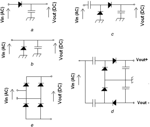
Different rectifier topologies
a Series
b Shunt
c Single-stage doubler
d Greinacher
e Bridge [5]
In [14], we presented an RF-DC converter system specifically developed to harvest energy from the GSM 900/1800 bands with the help of a textile wearable dual-band antenna. Through computer simulations, we designed and evaluated a five-stage Dickson voltage multiplier. A voltage multiplier converts alternating current power from a lower voltage to a higher DC voltage using a network of capacitors and diodes. During the fabrication of a prototype with COTS components, we noted that different printed circuit board fabrication techniques resulted in different values of conversion efficiency. Hence, we built three different prototypes referred to as Prototypes 1, 2 and 3, (Fig. 2) and measured their characteristics.
Figure 2.
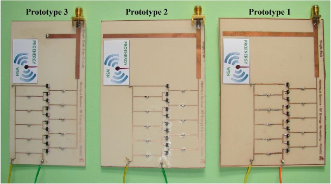
Prototypes of five-stage Dickson multipliers with impedance matching circuit
Figs. 3 and 4 show the output voltage and the conversion efficiency, respectively, of the prototypes with a load impedance of 100 kΩ in all cases. The superimposed simulation results in these figures were obtained through a harmonic balanced analysis, that is, a frequency domain method that evaluates the steady-state solution of a non-linear circuit. Two levels for VoutDC are particularly highlighted by solid lines in Fig. 3, namely the minimum and recommended voltage required to power a wearable sensor, 1.8 and 3 V, respectively, which allows for assessment of the sensitivity. Table 1 presents the measured sensitivity values for VoutDC = 1.8 V for the three prototypes. The maximum conversion efficiency, η0max, and maximum harvested power for a load impedance of 100 kΩ, that is, the power dissipated in the load, P0max, are also presented in Table 1. Note that Prototype 2 has the highest η0max and P0max, as well as the best sensitivity. For the sake of comparison, the RF harvester in [5] exhibited a measured sensitivity of more than 10 dBm for VoutDC = 1.8 V in the two-tone operation mode, with RL = 10 kΩ. Hence, our proposed prototypes represent significant improvement due to the use of a voltage multiplier.
Figure 3.
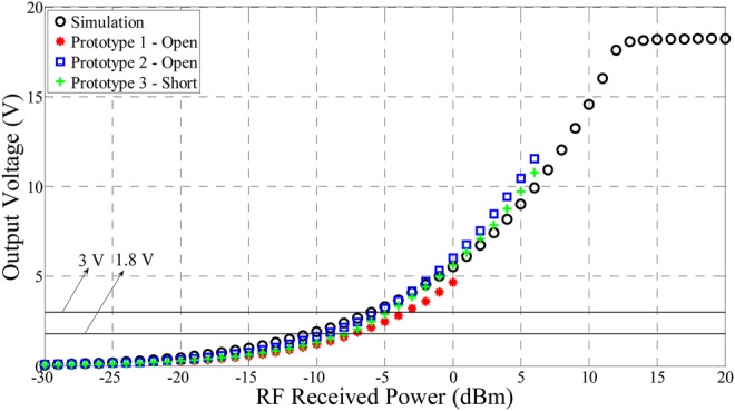
Output voltage as a function of RF received power
Figure 4.
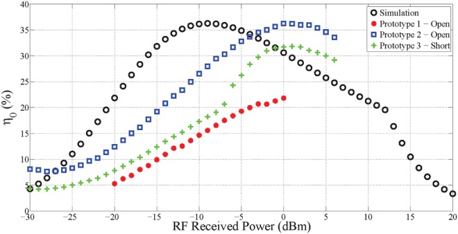
Conversion efficiency as a function of RF received power
Table 1.
Characteristics of the RF-EH prototypes developed in [14]
| RF-EH circuit | Sensitivity | Maximum η0max | Maximum P0max |
|---|---|---|---|
| Prototype 1 | −7 dBm for VoutDC = 1.8 V | 22% at PRF = 0 dBm | 0.22 mW at PRF = 0 dBm |
| Prototype 2 | −9 dBm for VoutDC = 1.8 V | 36% at PRF = 0 dBm | 1.33 mW at PRF = 6 dBm |
| Prototype 3 | −8 dBm for VoutDC = 1.8 V | 32% at PRF = 1 dBm | 1.16 mW at PRF = 6 dBm |
Since the objective is to harvest the highest amount of energy from the EM spectrum, we propose other Dickson voltage multipliers prototypes to harvest EM energy from the 700 MHz digital terrestrial television (DTT) frequency band. We have developed RF EH and antennas to operate within these frequency bands (750–758 MHz), with a centre frequency band of 754 MHz, due to the potential arising from the wide/broad deployment of DTT in Portugal.
In order to choose how many stages should be considered in the design of these prototypes regarding the centre frequency of 754 MHz, the use of two types of analysis is considered in the advanced design system (ADS) simulation software – the harmonic balanced analysis and the transient analysis. The analysis consisted of simulating the circuits with different numbers of stages, N, i.e., N = 3, 4, 5, 6, 7, 8, 9, 10, and with an impedance load of 100 kΩ, with and without the respective impedance matching stub. For each N-stage Dickson voltage multiplier circuit, the corresponding open-circuit stub impedance matching was dimensioned by means of the Smith Chart and Linecalc utilities from ADS.
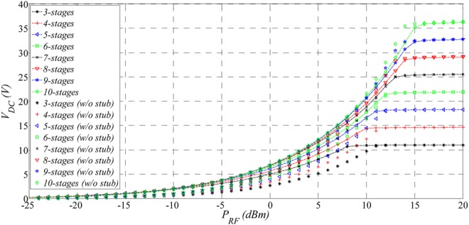
Fig. 5 depicts the simulations results regarding the impact of the RF received power (PRF) on output voltage (VDC) for an N-stage Dickson voltage multiplier with a load impedance of 100 kΩ (with and without impedance matching). For low receiving power (−50 to −25 dBm) the output voltage is negligible .
Figure 5.
Output voltage as a function of RF received power for N-stages Dickson voltage multipliers within DTT band
For RF received powers higher than −25 dBm (in the range from ) and number of stages up to 8, the output voltage is clearly lower without stub. As the number of stages increases, the difference in the output voltage between the cases with and without stub decreases.
However, the output voltage saturates beyond a certain value for the RF received power, depending on the number of stages from the Dickson voltage multiplier.
As, in Fig. 5, the output voltage is proportional to the number of stages. There are practical restrictions (i.e. diode current and prototype size) that limit the allowable number of stages from the Dickson voltage multiplier.
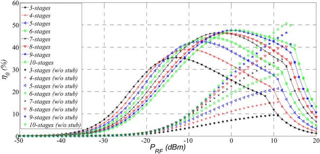
Fig. 6 presents the simulation results for the conversion efficiency (η0) as function of the received power, also for an N-stage Dickson voltage multiplier with a load impedance of 100 kΩ (with and without impedance matching). The analysis of these results allows us to decide the best number of stages for our new harvesting prototypes.
Figure 6.
Conversion efficiency as a function of RF received power for N-stages Dickson voltage multipliers within DTT band
By analysing Fig. 6, one observes the curves related to the cases that account for the impedance matching circuit and attain their maximum value for the efficiency value for lower values of the RF received power (i.e. PRF ≤ −13 dBm). Since the intention is to harvest energy at low RF received powers, the best choice should be a prototype that considers 5-stages, or even a prototype that considers 7-stages, since they present a good tradeoff between the output voltages and conversion efficiency at low RF powers.
In order to evaluate the performance from the prototypes of the 5- and 7-stages Dickson voltage multipliers with match impedance within the 700 MHz DTT band, different experimental tests have been performed. These tests have comprised the use of a Rohde & Schwarz signal generator that enables one to inject different values of RF power, in order to observe the DC voltage output.
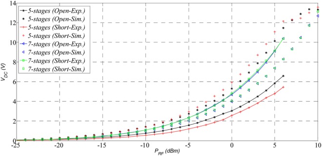
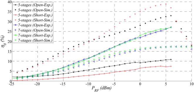
Figs. 7 and 8 show the simulation and experimental results for the output voltage and conversion efficiency, respectively, for the 5- and 7-stages Dickson voltage multipliers with match impedance (open and short circuit). From Fig. 7, one can observe that the experimental results for output voltages from the 5-stage prototypes are lower than simulation results. Additionally, the saturation of the output voltage from the prototypes is not observable since injecting higher RF received power into the prototype could damage and burn the HSMS-2850 Schottky diodes from the amplifier because of excessive current. Therefore in the experimental results the maximum RF received power is 6 dBm. In turn, for the 7-stage Dickson voltage multiplier, for the output voltage the experimental results obtained from the prototypes are higher than the values computed by means of simulation.
Figure 7.
Experimental and simulation results for output voltage as a function of received power within DTT band
Figure 8.
Experimental and simulation results for conversion efficiency as a function of received power within DTT band
In Fig. 8, one observes the maximum conversion efficiencies obtained experimentally are 10.9, 7.6, 27.1 and 27% for the 5-stages (open circuit), 5-stages (short circuit), 7-stages (open circuit) and 7-stages (short circuit), respectively. These maximum conversion efficiencies were attained at PRF = 6, 4, 6 and 6 dBm, respectively.
The difference between the simulation and experimental results from the conversion efficiency (Δη0) is at PRF = 6 dBm for the 5-stage Dickson voltage multiplier with open-circuit stub. In turn, the 5-stage Dickson voltage multiplier with short-circuit stub presents a difference at PRF = 6 dBm. Therefore experimental results of the conversion efficiency for the 5-stage Dickson voltage multiplier prototypes present a loss compared to the simulation results. For the 7-stage Dickson voltage multiplier with open- and short-circuit stubs, it is observable that the experimental conversion efficiency is clearly higher than the results obtained by means of simulation. The difference between the simulation and experimental results for the conversion efficiency is at PRF = 6 dBm for the 7-stage Dickson voltage multiplier with open-circuit stub. In turn, the 7-stage Dickson voltage multiplier with short-circuit stub presents a difference at PRF = 6 dBm. Hence compared with the simulation results, the experimental results for the 7-stage Dickson voltage multiplier prototypes present a conversion efficiency gain.
The objective is to store the energy in our RF-EH with super-capacitor storing system (presented ahead in Section 4) and then supply the wireless body area network (WBAN) node. There are two levels (i.e. 1.8 and 3 V) that are desirable to be attained by the prototypes in order to fulfil the requirements. The results are summarised as follows: the 5-stages multiplier with open-circuit stub reaches 1.8 V for PRF ≥ −4 dBm and reaches 3 V at PRF ≥ 0 dBm. The 5-stages multiplier with short-circuit stub reaches 1.8 V for PRF ≥ −2 dBm and reaches 3 V at PRF ≥ 1 dBm. The 7-stages with open-circuit stub reaches 1.8 V for PRF ≥ −7 dBm and reaches 3 V at PRF ≥ −3 dBm. In turn, the 7-stages multiplier with short-circuit stub reaches 1.8 V for PRF ≥ −4 dBm and reaches 3 V at PRF ≥ 0 dBm.
As a final remark and by observing the results obtained for the 5- and 7-stages Dickson voltage multipliers prototypes, the most suitable ones to harvest EM energy from the DTT frequency band are the 7-stages prototypes because of the higher efficiency that can be attained jointly with the output voltage that could be delivered. By comparing the results obtained for the 5-stage Dickson voltage multiplier prototypes at 945 MHz, as shown in Figs. 3 and 4, with the results from Figs. 7 and 8, it is notable that at 945 MHz, the output voltage and conversion efficiency is higher than at 754 MHz.
This is an expected result since the DTT frequency is lower than the GSM900 frequency. This leads to a decrease of the output voltage and conversion efficiency in the DTT EH prototypes.
However, since the 7-stage Dickson voltage multiplier prototypes have achieved higher experimental output voltage and conversion efficiency, compared to the simulation results, and the DTT transmitters are dedicated only to transmit the TV signal at a considerably higher power than GSM base stations, it is expected that the 7-stages multiplier prototypes will harvest more EM energy than the 5-stages prototypes, for GSM 900/1800 frequency.
4. RF-EH with super-capacitor storing system
After designing and developing the RF energy harvester, an additional goal is to use this energy to supply a WBAN node. The most common options to store energy are batteries. However, conventional rechargeable battery-based energy storage systems present some disadvantages by not allowing a precise estimation of the remaining energy while requiring a higher periodic maintenance, and having a limited number of recharge/discharge cycles, together with higher environmental impact when batteries are improperly disposed. Therefore the use of super-capacitors to store the harvested energy is one of the most suitable solutions.
In order to develop a super-capacitor storing system for the energy harvested from the EM waves, we propose a system, the different building blocks of which are presented in Fig. 9. The system is similar to that of Fahad et al. [15]. Instead of considering a solar panel as the energy source, we designed the circuit according to the RF energy harvester requirements. It consists of three main blocks: the front end, to manage, control and transfer the energy from the RF energy harvester(s) into the super-capacitor(s), a front-end control unit, which manages/controls the algorithm for the front-end, and embedded system blocks, i.e., the corresponding WBAN node to be powered-up.
Figure 9.
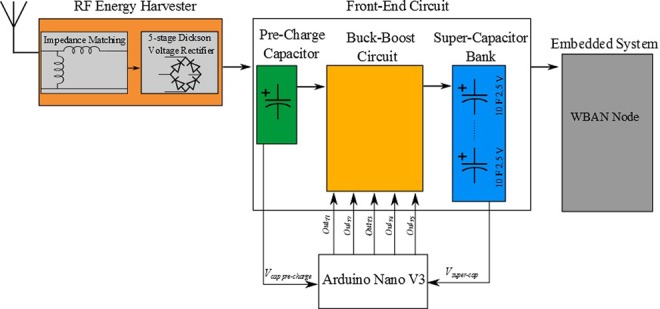
Block diagram of RF EH with super-capacitor storing system
Since the output voltage from the RF energy harvester depends on the quantity of cellular communications traffic or on the DTT power in the scavenging area, there is the need to control the voltage that is delivered to pre-charge capacitor from the front-end circuit. The minimum voltage that the pre-charge capacitor, Vcappre-charge, needs to achieve in order to initiate the procedure from the buck–boost circuit is 1.8 V, whereas the maximum voltage must be no more than the voltage the super-capacitor bank is designed for. In terms of voltage supply, the buck–boost circuit will take a maximum tolerance of , while the maximum output ripple will be at most 2%.
In Fig. 9, the front-end circuit is controlled by an ATMEL 328P microcontroller. The power source of the microcontroller is not shown here but the intention is to the use a pre-charged 1000 µF capacitor. The microcontroller makes use of the energy stored in the dedicated capacitor to power-up itself while it controls the energy flow from the RF energy harvester to the super-capacitor bank.
After it achieves a stable voltage in the super-capacitor bank and the dedicated capacitor drains all the energy, then the microcontroller starts using the energy stored in the super-capacitor bank in order to self-sustain its management activity.
Tests were performed to assess the average voltage that each RF energy harvester prototype is able to deliver when placed in different traffic GSM environments. From these field trials, we concluded that the minimal voltage to deliver to the buck–boost circuit is 1.8 V. The pre-charge capacitor voltage Vcappre-charge is controlled and supervised by the microcontroller and allows for transferring the accumulated energy into the super-capacitor(s) bank in small bursts.
This energy transfer is accomplished by the front-end circuit controlled by the microcontroller, which is set to work in buck converter mode [16] when the Vcappre-charge is higher than the voltage at the terminal of the super-capacitor(s) bank denoted as Vsuper-cap. In turn, the front-end circuit switches to boost mode when Vcappre-charge ≤ Vsuper-cap + Vloss, where Vloss is the voltage losses observed in the transistors and diodes. After each energy transfer cycle the Vcappre-charge voltage drops for an amount of voltage denoted as ΔVtransfer.
To find the most suitable values for the electronic components of the buck–boost converter, different experiments have been conducted to find the best transition times for charging the pre-charge capacitor and the duration of the energy transfer from the pre-charge capacitor to the inductor and from the inductor to the super-capacitor(s) bank. After finding the most suitable parameters for the electronic components as well as the transition times, the microcontroller firmware that is currently implemented has features that allow for employing an adaptive duty cycle management control algorithm. This algorithm is useful when the output voltage from the RF energy harvester(s) is higher than 1.8 V since it adapts the transition times between the pre-charge capacitor, inductor and super-capacitor(s) in order to increase the energy transfer.
To test the RF-EH with super-capacitor storing system, the 7-stage Dickson voltage multiplier (open stub) was considered as the EH prototype to be evaluated at different input power levels while considering a frequency of 754 MHz in the signal generator, as shown in Fig. 10. The output power from the signal generator was adjusted to three power levels, i.e., −10, −5 and −2 dBm, staying in each power level for about 22 550 s and then taking the Vsuper-cap average voltage at a frequency of 50 samples/s. Fig. 11 shows the voltage building up in the super-capacitor(s) bank as a function of time for different received powers generated by the signal generator. It is observable that the voltage in the super-capacitor(s) at the beginning of the experiment is 0 V and increases with time, as expected.
Figure 10.
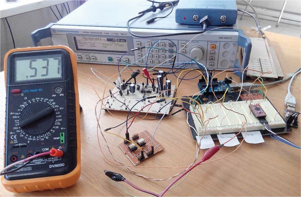
DTT RF energy harvester prototype experimental apparatus
Figure 11.
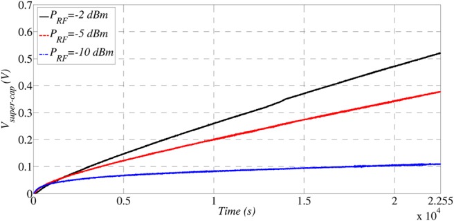
Voltage in super-capacitor(s) bank from DTT RF energy harvester for different values of received power as a function of time
It is observable that for a PRF = −10 dBm the curve presents a slight growing compared to the other curves. The curve that achieves the highest voltage after elapsing the experiment time is the one corresponding to the PRF = −2 dBm.
This result is expectable, because of the behaviour of the voltage output from the RF energy harvester for different received powers. The explanation is as follows: VDC = 3.61, 2.34 and 1.436 V for PRF = −2, −5 and −10, respectively. The maximum voltages attained in the super-capacitor(s) are Vsuper-cap = 0.5199, 0.3758 and 0.1075 V at PRF = −2, −5 and −10 dBm, respectively.
Fig. 12 presents the multi-band GSM and DTT RF energy harvester block diagrams that combine the energy harvested from an RF energy harvester for the GSM band jointly with the energy harvested from an RF energy harvester for the DTT band. For each RF energy harvester, there is an impedance matching circuit that filters the frequency band intended for the prototype. The power received within the GSM and DTT band is denoted by PRF_IN1 and PRF_IN2, respectively. After filtering the signal by means of the impedance matching circuits, the received power at the GSM and DTT RF energy harvester is attenuated by factors α1 and α2, respectively. In the literature [17], it is mentioned that this loss could be at most 3%. The received powers, α1PRF_IN1 and α2PRF_IN2, are then rectified by means of 5- and 7-stage Dickson voltage rectifiers, which results in a DC voltage in the output of RF energy harvester. In order to take advantage of all the RF energy that is scavenged from each of the frequency bands, both output voltages, VDC_IN1 and VDC_IN2, are combined into the total output voltage from the multi-band RF energy harvester, i.e., VDC_sum. The total output voltage is delivered to the front-end circuit (i.e. buck–boost circuit) which is controlled by a power management unit. This unit acquires the different voltages at different stages of the buck–boost converter and manages the transfer of the energy received from the multi-band RF energy harvester to the storage unit (composed by super-capacitors). The voltage variation associated to the energy transfer between the buck–boost converter and storage unit is denoted by VIN_Buck in Fig. 12. Finally, the energy stored is transferred to the load, which in this case is represented by a WBAN node. The voltage variation associated to the discharge from the storage unit is denoted as VOUT, as shown in Fig. 12.
Figure 12.
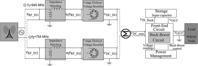
Multi-band GSM and DTT RF energy harvester block diagram
5. Conclusion
RF-EH is becoming a mature technology with the enormous potential to realise the vision for uninterrupted self-powered networks of biomedical sensors, capable of perpetual monitoring of patients’ vital signs. In the last years, there has been an effort to evolve the RF-EH devices in terms of scavenging RF energy from various commercial wireless communication systems. In this Letter, different and important observations have been reported concerning the different RF-EH devices as well as the energy storing systems that can be used to store the energy for posterior use by a WBAN node. Regarding the RF-EH device, the GSM 900/1800 bands provide the highest power density for RF-EH in urban and suburban environments. Improvement in the conversion efficiency and sensitivity of rectennas for these frequency bands is one of the biggest challenges. By comparing the obtained results with the ones for the DTT RF-EH, it is notable that the RF-EH device for the GSM band presents an output voltage and conversion efficiency higher than the DTT RF-EH device. This is an expected result since the DTT frequency is lower than the GSM 900/1800 frequency, which leads to a diminishing of the output voltage and conversion efficiency in the DTT EH prototypes. However, since the DTT RF-EH prototypes achieved better results in terms of output voltage and conversion efficiency (compared to the simulation results) and the DTT transmitters are only dedicated to transmit TV signal at higher power levels than GSM base stations, it is expected that the DTT RF-EH prototypes will be more capable to harvest EM energy than the GSM RF-EH prototypes. As a future work, the increase of test duration will be considered, in order to observe how the energy builds up in the super-capacitor(s) bank and when the super-capacitor(s) bank is pre-charged with a certain voltage. In addition, tests will be performed with the multi-band GSM and DTT RF energy harvester, scavenging together RF energy with the respective antenna to the super-capacitor storing system in a real-environment scenario to observe how the energy builds up.
6. Acknowledgments
Special thanks to Henrique Saraiva.
7. Funding and declaration of interests
This work was supported by the PEst-OE/EEI/LA0008/2013, UID/EEA/50008/2013, the European Social Fund, PROENERGY-WSN, INSYSM, CREaTION, HANDCAD, ECOOP, ORCIP, EFAtraS and COST IC1004. Conflict of interst: none declared.
8 References
- 1.World Health Organization: ‘The global burden of chronic’. Available at http://www.who.int/nutrition/topics/2_background/en/, accessed 6th October 2014
- 2.Hanson M.A., Powell H.C., Jr., Barth A.T., et al. : ‘Body area sensor networks: challenges and opportunities’, Computer, 2009, 42, (1), pp. 58–65 (doi: ) [Google Scholar]
- 3.Lo B., Thiemjarus S., Panousopoulou A., Yang G.-Z.: ‘Bioinspired design for body sensor networks [life sciences]’, IEEE Signal Process. Mag., 2013, 30, (1), pp. 165–170 (doi: ) [Google Scholar]
- 4.Gündüz D., Stamatiou K., Michelusi N., Zorzi M.: ‘Designing intelligent energy harvesting communication systems’, IEEE Commun. Mag., 2014, 52, (1), pp. 210–216 (doi: ) [Google Scholar]
- 5.Kuhn V., Seguin F., Lahuec C., Person C.: ‘A multi-tone RF energy harvester in body sensor area network context’. Loughborough Antennas and Propagation Conf., Loughborough, UK, November 2013, pp. 238–241 [Google Scholar]
- 6.Barroca N., Saraiva H.M., Gouveia P.T., et al. : ‘Antennas and circuits for ambient RF energy harvesting in wireless body area networks’. IEEE Int. Symp. Personal, Indoor and Mobile Radio Communications, London, UK, September 2013, pp. 532–537 [Google Scholar]
- 7.Piñuela M., Mitcheson P.D., Lucyszyn S.: ‘Ambient RF energy harvesting in urban and semi-urban environments’, IEEE Trans. Microw. Theory Tech., 2013, 61, (7), pp. 2715–2726 (doi: ) [Google Scholar]
- 8.Visser H.J., Reniers C., Person A.C.F., Theeuwes J.A.C.: ‘Ambient RF energy scavenging: GSM and WLAN power density measurements’. European Microwave Conf., Amsterdam, The Netherlands, October 2008, pp. 721–724 [Google Scholar]
- 9.Valenta C.R., Durgin G.D.: ‘Harvesting wireless power: survey on energy-harvester conversion efficiency in far-field, wireless power transfer systems’, IEEE Microw. Mag., 2014, 15, (4), pp. 108–120 (doi: ) [Google Scholar]
- 10.Mandal S., Turicchia L., Sarpeshkar R.: ‘A low-power, battery-free tag for body sensor networks’, IEEE Pervasive Comput., 2010, 9, (1), pp. 71–77 (doi: ) [Google Scholar]
- 11.Zhang X., Jiang H., Zhang L., Zhang C., Wang Z., Chen X.: ‘An energy-efficient ASIC for wireless body sensor networks in medical applications’, IEEE Trans. Biomed. Circuits Syst., 2010, 4, (1), pp. 11–18 (doi: ) [DOI] [PubMed] [Google Scholar]
- 12.Xia L., Cheng J., Glover N.E., Chiang P.: ‘0.56 V, − 20 dBm RF-powered, multi-node wireless body area network system-on-a-chip’, IEEE J. Solid-State Circuits, 2014, 49, (6), pp. 1345–1355 (doi: ) [Google Scholar]
- 13.Dini M., Filippi M., Costanzo A., et al. : ‘A fully-autonomous integrated RF energy harvesting system for wearable applications’. European Microwave Conf., Nuremberg, Germany, October 2013, pp. 987–990 [Google Scholar]
- 14.Borges L.M., Barroca N., Saraiva H.M., et al. : ‘Design and evaluation of multi-band RF energy harvesting circuits and antennas for WSNs’. Proc. 21st Int. Conf. Telecommunications, Lisbon, Portugal, May 2014, pp. 308–312 [Google Scholar]
- 15.Fahad A., Soyata T., Wang T., Sharma G., Heinzelman W., Shen K.: ‘Solarcap: super capacitor buffering of solar energy for self-sustainable field systems’. Proc. of the 2012 IEEE Int. SOC Conf. (SOCC), Niagara Falls, NY, USA, September 2012, pp. 236–241 [Google Scholar]
- 16.Pressman A.: ‘Switching power supply design’ (McGraw-Hill, Inc, New York, NY, USA, 1998, 2nd edn.) [Google Scholar]
- 17.Pavone D., Buonanno A., D'Urso M., Corte F.D.: ‘Design considerations for radio frequency energy harvesting devices’, Prog. Electromagn. Res. B, 2012, 45, pp. 19–35 (doi: ) [Google Scholar]


