

Abstract
Carbon nanomaterials are advantageous as electrodes for neurotransmitter detection, but the difficulty of nanomaterials deposition on electrode substrates limits the reproducibility and future applications. In this study, we used plasma enhanced chemical vapor deposition (PECVD) to directly grow a thin layer of carbon nanospikes (CNS) on cylindrical metal substrates. No catalyst is required and the CNS surface coverage is uniform over the cylindrical metal substrate. The CNS growth was characterized on several metallic substrates including tantalum, niobium, palladium, and nickel wires. Using fast-scan cyclic voltammetry (FSCV), bare metal wires could not detect 1 μM dopamine while carbon nanospike coated wires could. The highest sensitivity and optimized S/N ratio was recorded from carbon nanospike-tantalum (CNS-Ta) microwires grown for 7.5 minutes, which had a LOD of 8 ± 2 nM for dopamine with FSCV. CNS-Ta microelectrodes were more reversible and had a smaller ΔEp for dopamine than carbon-fiber microelectrodes, suggesting faster electron transfer kinetics. The kinetics of dopamine redox were adsorption controlled at CNS-Ta microelectrodes and repeated electrochemical measurements displayed stability for up to ten hours in vitro and over a ten day period as well. The oxidation potential was significantly different for ascorbic acid and uric acid compared to dopamine. Growing carbon nanospikes on metal wires is a promising method to produce uniformly-coated, carbon nanostructured cylindrical microelectrodes for sensitive dopamine detection.
Introduction
Carbon-fiber microelectrodes (CFMEs) are the standard electrodes for neurotransmitter detection using fast scan cyclic voltammetry (FSCV) because of their biocompatibility, relatively small size, and high overpotential for water oxidation.1,2,3 Recently, there has been an interest in developing carbon nanomaterial based microelectrodes as alternatives to CFMEs because they have high sensitivity, anti-fouling properties, and higher conductivity which can lead to fast-electron transfer kinetics.4–6 For electrochemistry, coating of a thin layer of nanomaterial on the surface is ideal and maximizing the number of defect sites can lead to better signals for adsorption-controlled species. For example, vertically-aligned carbon nanotubes (CNTs) are advantageous because the defect-rich nanotube ends provide sites for the adsorption of neurotransmitters such as dopamine to the surface.5 New fabrication methods for growing carbon have led to many other carbon nanomaterials, such as carbon nanohorns, carbon nanofibers, and forms of graphene that may be advantageous for neurotransmitter electrochemistry.6 However, for carbon nanomaterial based electrodes to become a standard material for microelectrodes a facile, a batch fabrication method is needed that produces a reproducible, nanostructured surface that is electroactive for dopamine.
Carbon nanomaterials are often grown with thermal chemical vapor deposition (CVD), where the high temperatures supply the energy needed for chemical reactions. Substrates typically have a catalyst that guides the growth of the carbon. Shang et al. reported multilayered graphene nanoflake film on silicon substrate for the simultaneous detection of dopamine, ascorbic acid, and uric acid.7 The uniform nanoflake film synthesized by microwave plasma enhanced CVD was catalyst-free and resulted in an abundant, highly-graphitized knife-edge structure. Claussen et al. applied multilayered graphene petal nanosheets produced by CVD as substrates for sensitive electrochemical biosensing of glucose with association of platinum particle and Poly(3,4-ethylenedioxythiophene).8 The nanoflakes and nanopetals are advantageous for sensors because they have high surface areas for electron transfer.
Plasma-enhanced chemical vapor deposition (PECVD) is useful to help orient and direct carbon growth because the high energy electrons formed provide energy for chemical reactions at lower temperatures and the electric field aligns the structures.9 The Meyyappan group used PECVD to grow vertically aligned carbon nanofibers (CNFs) using a nickel catalyst,10 and these CNFs have been used for electrophysiological11,12 and electrochemical measurements.13–16 Thin films of carbon with petal-like nanostructures have been grown on Si with microwave enhanced PECVD17 as well as hot filament CVD18 and arc discharge.19 These petal-like sheets are only 20 nm thick and have sharp edges and a high surface to volume ratio. Sheridan et al. recently grew a similar type of carbon film on Si without the use of a catalyst.20 They termed their films carbon nanospikes (CNSs) because they consist of tapered, spike-like features less than 50 nm in diameter. CNS films had good electrochemical properties for oxygen reduction, comparable to glassy carbon electrodes.20 Deposition of catalyst is one of the most difficult parts of reproducible carbon nanomaterial growth.21 CNS films could be advantageous for coating difficult substrates, such as cylindrical wires, where catalyst deposition could limit the ability to completely coat a substrate. However, the electrochemical properties of other molecules, such as neurotransmitters, have not been characterized on CNS surfaces.
In this study, we grew carbon nanospikes on small, cylindrical metal wires to create microelectrode sensors. This is the first time that carbon nanospikes have been grown on metals or on cylindrical substrates. Using PECVD, the amount of carbon growth and the morphology of the carbon was dependent on both the metal substrate and the growth time. The growth of CNSs on metal wires has many advantages including (1) no catalyst is required for growth, (2) the carbon grows uniformly over the entire metal, (3) the metal substrate is conductive and will not limit the signal transduction of electron transfer, and (4) there is no requirement of an insulating barrier for catalyst deposition so there is direct electrical contact between the carbon nanospikes and substrate. The electrochemical properties of the CNS-coated metal wire microelectrodes were characterized for dopamine detection using fast-scan cyclic voltammetry (FSCV). While all of the coated metal microelectrodes could detect dopamine redox, CNS-Tantalum (CNS-Ta) microelectrodes had faster electron transfer kinetics and a lower limit of detection than any of the other CNS-metal microelectrode or standard CFMEs. The CNS-Ta microelectrodes showed adsorption-controlled behavior for dopamine, good stability, and relatively high sensitivity compared to other microelectrodes with FSCV. Growing CNS on Ta microwires is a promising strategy for batch fabricating nanostructured electrodes for neurotransmitter measurements.
Methods and Materials
Chemicals and Materials
Dopamine was purchased from Sigma (St. Louis, MO). A 10 mM stock solution was prepared in 0.1 M perchloric acid and diluted to 1.0 μM daily with phosphate-buffered saline (PBS) (131.5 mM NaCl, 3.25 mM KCl, 1.2 mM CaCl2, 1.25 mM NaH2PO4, 1.2 mM MgCl2, and 2.0 mM Na2SO4 with the pH adjusted to 7.4). All aqueous solutions were made with deionized water (EMD Millipore, Billerica, MA). Armstrong C7 Resin and Armstrong A2 Activator were obtained from Ellsworth Adhesives (Germantown, WI). Diethylenetriamine hardener (DETA) was used as received from Fisher Scientific (Waltham, MA).
Instrumentation
Fast scan cyclic voltammetry (FSCV) was performed using a ChemClamp potentiostat (Dagan, Minneapolis, MN). Data were collected and analyzed with Tarheel CV software (gift of Mark Wightman, UNC) using custom data acquisition hardware previously described.22 A triangle waveform was applied to the electrode from a holding potential of −0.4 V to 1.3 V and back at a scan rate of 400 V/sec and a frequency of 10 Hz, unless otherwise noted. A silver-silver chloride wire was used as the reference electrode. Samples were tested in a flow injection analysis system consisting of a six-port, stainless steel HPLC loop injector mounted on a two-position air actuator (VICI Valco Instruments, Co., Houston, TX). Buffer and samples were pumped through the flow cell at two mL/min unless otherwise noted using a syringe pump (Harvard Apparatus, Holliston, MA).
Plasma Enhanced Chemical Vapor Deposition
Metal wires (ESPI Metal, Ashland, OR) approximately 25 μm in diameter were cut into pieces 3 to 5 cm in length. Metal wires were attached to a stainless steel stage which was placed into a custom built DC plasma-enhanced chemical vapor deposition chamber. During growth, the metal wires served as the cathode for the DC plasma. In the chamber (6 Torr chamber pressure), the wires were exposed to 100 sccm (standard cubic centimeters per minute flow rate) ammonia and 80 sccm acetylene for 3.5, 5, 7.5, 15, or 30 minutes. The DC plasma discharge was operated at 250 mA and 480–550 V at 650°C.
Scanning Electron Microscopy (SEM)
SEM images were taken with a ZEISS Merlin SEM microscope with a secondary electron detector using an accelerating voltage of 5 kV and a working distance of 5.6 mm.
Electrode Construction
Epoxy-insulated microelectrodes were formed as previously described.23 A 2 cm thick Teflon block (McMaster Carr, Atlanta, GA) was cut into rectangles. Channels (~70–80 μm thick, ~70–80 μm deep, and 2–6 cm long) were formed by laser etching the Teflon mold with a CO2 engraving machine (Versa Laser® 350 with High Power Density Focusing Optic lens unit, Universal Laser Systems, Scottsdale, AZ, USA). Under a stereoscope, epoxy (Armstrong Resin C7 and 0.8% Activator A2) was placed in each channel using a syringe with a 30 gauge needle. Metal wires were laid manually into each channel, and the wires were pulled from the back to allow approximately 100 μm of the tip to protrude. The epoxy was cured for three hours at 165°C and then electrodes removed from the channels. The non-electrode end of the metal wire was connected to a gold pin (0.035″ × 0.249″, Digikey, Thief River Falls, MN) by silver epoxy (H20E, equal portions of Parts A and B, Epoxy Technology, Billerica, MA) to facilitate connection to the potentiostat. The silver epoxy was cured for one hour at 150°C.
Results
Surface Characterization
PECVD was used to synthesize thin films of carbon nanospikes.17 The carbon nanostructures on different types of metals were characterized with SEM (Fig. 1). Distinct ridges and grooves are observed on the bare metal tantalum wire, which is 25 μm in diameter (Fig. 1A). After carbon nanospike growth for 7.5 min with PECVD, the surface is nanostructured but the diameter of the wire is not significantly increased (Fig. 1B). At high resolution, the surface has distinct, high-aspect ratio spike-like or petal-like features less than 10 nm in length (Fig. 1C). These features are aligned and stick up from the surface of the electrode. The nanospikes have a high aspect ratio, which is advantageous for detection of adsorbed species. The cylindrical wire is completely covered with the CNS film. The growth looks similar to previous studies on Si which saw petal-like carbon flakes approximately 5–10 nm in length.17
Figure 1.
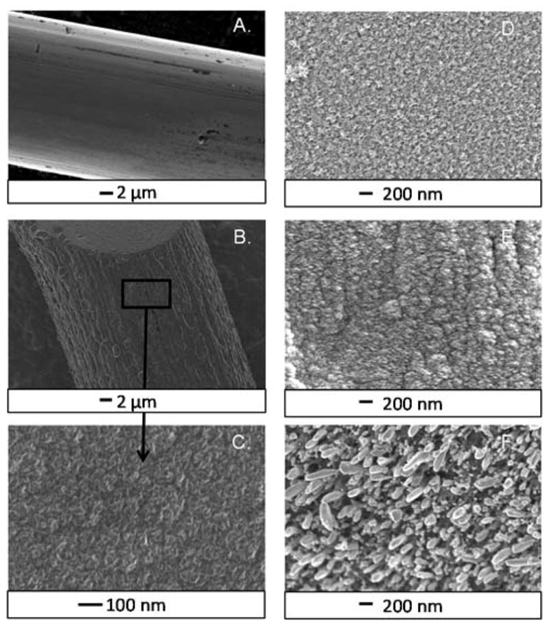
Carbon nanospike (CNS) surfaces (7.5 min growth time). A. SEM of a bare tantalum wire shows distinct grooves and ridges of rough metal surface. B. CNS-coated Ta wire (CNS-Ta) shows no noticeable increase in diameter. C. High magnification of carbon nanospikes grown on Ta wire. There is uniform coverage of aligned carbon spikes over the entire metal wire. D. High magnification of CNSs on Pd wire shows similar features. E. Nb wire also has aligned growth of small carbon spikes. F. Carbon grown on Ni wire has much larger surface features than the other metals. The ends of these features are rounded.
CNS growth was compared on tantalum (Ta), palladium (Pd), niobium (Nb), and nickel (Ni) wires. The CNSs on the surface of Pd (Fig. 1D) and Nb (Fig. 1E) metal wires have similar structures and feature sizes to the Ta wires grown with CNSs. However, the features on the Ni wires were much larger and had a different, more rounded structure (Fig. 1F). The feature size on the Ni surface is similar to carbon nanofibers.24 No catalyst was used for any of the metal wires, but Ni is a popular catalyst for growing CNTs and carbon nanofibers,13 so it may have catalytic effects that affected the feature size of the growth. Thus, the type of growth is dependent on the metal substrate.
Raman spectra were collected for each of the CNS-metal wire samples (Fig. 2). The G band (1580 cm−1) is due to the coplanar vibration of sp2 bonded carbon atoms and the D band (1340 cm−1) is due to graphene defects and disorders.2 The area under the peak is calculated and the ratio between the D and G band area is widely used to evaluate the quality of carbon nanomaterials.3 As shown in Fig. 2, the D/G ratio was smallest for CNS-Ta at 2.3 and largest for CNS-Pd at 4.4. The D/G ratio for Ni or Nb was in between Ta and Pd; it was 3.1 for CNS-Ni and 3.2 for CNS-Nb. Thus, the CNS-Ta electrode was less defect rich than the other CNS samples. However, the CNS growth on metal substrates is relatively edge-plane rich compared to the multilayer graphene sheets reported previously.25
Figure 2.

Raman spectrum of carbon nanospikes grown on A. tantalum, B. palladium, C. niobium, and D. nickel wires.
Background Charging Currents
Background charging currents are a function of capacitance, scan rate, surface functional groups, and electrode area. Charging currents were compared for bare metal wires (Fig. 3A) and the carbon nanopsike grown wires (Fig. 3B). All the metal wire electrodes are geometrically about the same area, with 25 micron diameter wire and 100 micron exposed length. The background charging currents of bare Ta, Pd, and Nb wires are nearly square, which indicates that they are mainly capacitive with little surface functionalization (Fig. 3A).3 Pd has higher background currents than any of the other metals. The background charging current of Ni is smaller and the non-square shape indicates that it is not a simple capacitive current, although it does not resemble typical carbon-based electrode charging currents. The higher current around the switching potential for Ni may indicate water oxidation.22
Figure 3.

Background charging currents. A. Background charging currents of bare metal wire electrodes. The rectangular shape of most of the metal wires is indicative of an ideal capacitor with the exception of the irregular shape of Ni. B. Background currents of CNS coated metal wire electrodes with a 7.5 minute growth time. After CNS coating, the background currents change in shape and increase in magnitude.
Charging currents are proportional to the amount of carbon on the surface and can be used to monitor the extent of carbon nanospike growth on a particular metal. After 7.5 min of PECVD coating, the carbon nanospike-modified wires have background currents which are 5 to 25 fold larger than bare wires (Fig. 3B). The large increase in capacitive charging current indicates an increase in surface area due to increased surface roughness, as well as electron transfer associated with the solution-surface functional group interface.4 The shape of the background current also changes after carbon coating; for example, tantalum has more of a curve around 0.6 V that is indicative of surface oxide groups on a carbon surface.26 After the voltage waveform has been applied to a CNS coated metal electrode for thirty minutes for equilibration, the background current is similar in shape to that of carbon-fiber electrodes.4
Detection of Dopamine
The FSCV response to 1 μM dopamine was compared between bare metal wire electrodes (Fig. 4A) and CNS-coated metal wire electrodes (Fig. 4B). The background-subtracted cyclic voltammograms for bare tantalum and palladium wire electrodes have small, square responses with no faradaic peaks (Fig. 4A). These currents are likely just small errors due to imperfect background subtraction. Bare nickel and niobium wire electrodes have small peaks close to the switching potential, but these are at higher potentials than typically observed for dopamine oxidation at carbon electrodes.26 The shapes of the peaks are not particularly symmetrical, and these small peaks are likely to be due to background drift or background subtraction errors.
Figure 4.

Detection of dopamine. A. Detection of 1 μM dopamine with bare metal electrodes. No characteristic dopamine peaks are seen in the background-subtracted cyclic voltammograms and the currents are very low. B. Detection of 1 μM dopamine with carbon nanospike-grown metal wire electrodes. Carbon nanospikes were grown for 7.5 min with PECVD for all wires, and the exposed tip for the microelectrode was 100 μm.
The background-subtracted cyclic voltammograms for 1 μM dopamine at CNS-coated metal wire electrodes are characteristic of dopamine detection (Fig. 4B).27 Ta and Pd have markedly higher currents for dopamine than Nb or Ni, even though all wires have the same exposed area and growth conditions. The CNS-Nb wire has some additional capacitance in the signal as well as the dopamine redox peaks. The CNS-Ni wire has an extra peak at the switching potential, similar to the extra peak observed in the background current. The kinetics of dopamine detection differed among the wires, as the ΔEp (peak separation) for CNS-Ta was less than other CNS grown wires, making them attractive as electrode materials.
Table 1 compares average electrochemical data for dopamine detection at carbon-fiber microelectrodes and carbon nanospike-modified wire microelectrodes. CNS-metal wire electrodes in general have lower limits of detection, faster electron transfer kinetics, and smaller reduction to oxidation ratios than CFMEs. The ΔEp values for all CNS-metal wires are smaller than CFMEs (one-way ANOVA with Bonferroni’s post-test, p<0.0001) with the exception of Pd (p =0.62). The peaks are about 100 mV closer together for CNS-Ta electrodes than for carbon fibers. Higher conductivity may lead to better electron transfer kinetics and metal wires have higher conductivities than carbon fibers.1,28 However, the ΔEp did not follow the same trend as metal conductivity. Ni has the lowest conductivity of the metals tested and, yet, CNS-coated Ni has a similar ΔEp to the higher conductivity Nb and Ta wires. Thus, the underlying conductivity of the wire did not seem to be a big factor in electron transfer kinetics, and electron transfer is likely limited by the CNS coating.
Table 1.
Electrochemical Data. A chart of the limit of detection for dopamine, ΔEP, and ratios of peak oxidative to peak reductive currents comparing CFMEs to Ta, Pd, Ni, and Nb CNS coated metal wires (7.5 minutes growth).
| Material | LOD (nM) (n = 6) | ΔEP (V) (n =6) | I p,c/I p,a(n = 6) |
|---|---|---|---|
| Carbon Fiber23 | 24 ± 2 | 0.67 ± .02 | 0.56 ± 0.04 |
| Ta-CNS | 8 ± 2* | 0.55 ± .03* | 0.83 ± 0.06* |
| Pd-CNS | 27 ± 2 | 0.70 ± .03 | 0.83 ± 0.10* |
| Nb-CNS | 12 ± 2* | 0.59 ± .05* | 0.91 ± 0.10* |
| Ni-CNS | 16 ± 3* | 0.58 ± .02* | 0.97 ± 0.06* |
CNS-wire electrode is significantly different than CFMEs (p<0.05)
CNS metal wire electrodes, with the exception of Pd, had lower limits of detection than CFMEs (Table 1, one-way ANOVA with Bonferroni post-test, p < .0001). The protruding length of all wires was 100 μm; however, the CNS coated wires were 25 μm diameter while CFMEs are 7 μm diameter. Thus, the geometric area of the CFMEs is about 9 times smaller and the sensitivity for CFMEs (0.003 nA/μM·μm2) and CNS-Ta electrodes (average of 0.002 nA/μM·μm2) are similar. CNS-coated Pd wires had larger magnitude background charging currents, which correlates with higher noise.29 Although the oxidative currents for dopamine were large at CNS-Pd electrodes, the limits of detection were not as low. The larger backgrounds and noise may be due to the higher capacitance of the Pd metal.
Another interesting property of CNS coated metal electrodes is that the detection of dopamine is more reversible than at CFMEs, as demonstrated by the lower cathodic/anodic (Ip,c/Ip,a) peak ratios (Table 1, one-way ANOVA with Bonferroni post-test, p < 0.0001) for all CNS-coated wires compared to CFMEs. Dopamine oxidation is quasi-reversible at CFMEs; not all of the dopamine-o-quinone (DOQ) produced from dopamine oxidation is reduced back to dopamine. However, all four CNS-metal electrodes are more reversible than carbon fibers, and this property has also been observed at CNT-fiber and yarn based electrodes.6,30
Effect of Growth Time
We chose CNS-Ta electrodes to characterize further because of their high sensitivity, fast electron transfer kinetics, and good reversibility. The effect of growth time was tested on electrochemical current for dopamine. Stable sensors were obtained when the growth time was between 3.5 and 7.5 minutes. Figure 5 shows that the dopamine oxidation current is greater for 7.5 minute growth on Ta than for the other growth times (one-way ANOVA, p < .0001, n = 6). The current for CNS-Ta electrodes grown for 7.5 min was about 2.5-times larger than the current for electrodes grown for 5 minutes, and 18-times larger than for CNS-Ta electrodes grown for 3.5 minutes (Bonferonni post-tests, p > 0.05, n = 6). The background charging currents can be used to estimate surface area differences of CNS-Ta wire electrode with different growth times. The background charging current of the 7.5 minute growth time is about 3-times greater than the 5 minute growth time and 15-times greater the 3.5 minute growth. Thus, the increases in current are similar to the increases in background current. The differences in S/N ratio are more modest than the differences in background current because increased background current leads to more noise.29 The best S/N ratio for 1 μM dopamine was 123 ± 15 for the 7.5 minute samples, compared to 33 ± 2.5 for the 5 min sample and 19.3 ± 0.8 for the 3 min sample. The 7.5 minute growth time for CNS-Ta microelectrodes was considered optimal because it maximized the S/N ratio.
Figure 5.

Effect of Growth Time. The peak oxidative current for 1 μM dopamine was recorded for CNS-Ta electrodes grown for different times. Longer growth times lead to increased currents for dopamine (one-way ANOVA, Bonferonni post-test, p < .0001, n=6 each).
Longer growth times of 15 or 30 min were also investigated, but these times resulted in electrodes that were too noisy to use. The 30 minute samples had S/N ratios of 3.9 ± 1.0, significantly lower than the S/N for the 7.5 min growth time (t-test, p = 0.0001, n=6). SEM images of CNS-Ta with 15 min growth time reveal a different morphology of carbon, with more heterogeneous carbon and significantly more growth (Supp. Fig. 1). The diameter of the electrodes was twice as big as the diameter of the wire, indicating a thick film. The longer growth resulted in low S/N readings because there was more material to be charged with the applied voltage, but this material was not exposed to the analyte and thus did not increase the Faradaic signal. Previous studies with dip coating CNTs found that agglomerations on the surface caused high Faradaic currents, but low S/N ratios because the material was not accessible to dopamine to be detected.31
Adsorption Studies
The scan rate was varied from 100 to 1000 V/s, and Figure 6A shows the current for 1 μM dopamine increases linearly with respect to scan rate. This indicates that dopamine oxidation at CNS-Ta microelectrodes is an adsorption controlled process, similar to dopamine oxidation at CFMEs. Thus, it is likely to be dependent on the surface properties, including the surface oxide groups.32
Figure 6.
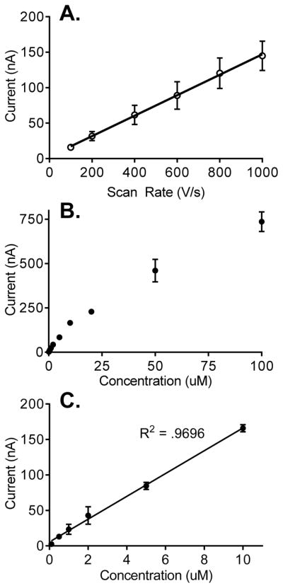
A. Effect of Scan Rate. A linear relationship was observed between scan rate and peak oxidative current for 1 μM dopamine at CNS-Ta electrodes, denoting adsorption control (n = 4, R2 = 0.90). B. Concentration study at CNS-Ta electrodes. Dopamine concentrations were varied from 100 nM to 100 μM. With concentrations higher than 10 μM dopamine saturates the surface of the electrode and detection becomes diffusion controlled. Error bars are standard error of mean (n = 4). C. Dopamine current is linear with concentrations up to 10 μM.
The concentration range for dopamine was tested for CNS-Ta electrodes using 100 nM to 100 μM dopamine (Fig. 6B). The dopamine oxidative current for CNS-Ta microelectrodes was linear up to 10 μM, similar to carbon-fiber microelectrodes (Fig. 6B).32 At concentrations higher than 10 μM, the adsorption sites on the surface of the CNS-Ta microelectrode become saturated, and the behavior is more diffusion controlled, which explains the deviation from linearity.32 Adsorption to the electrode surface is key for the sensitive detection of dopamine, particularly at carbon-fiber microelectrodes. 32 Bare metal wires do not have the carbon-oxygen functional groups and thus show little sensitivity for low concentrations of dopamine.3 The behavior for CNS coated electrodes is similar to CFMEs, indicating that the properties of carbon that are advantageous for dopamine adsorption and detection are present for this new type of carbon.
Selectivity and Stability
Ascorbic acid is an anion at physiological pH that can undergo a two-electron transfer oxidation.33 Uric acid is the final product of purine metabolism and acts as an antioxidant in cerebrospinal fluid and is also an anion at physiological pH.34 Dopamine, uric acid, and ascorbic acid usually coexist in the extracellular fluid of the central nervous system,35 so the ability to determine dopamine in the presence of uric acid and ascorbic acid is important. As indicated in Figure 7, the electrochemical responses of dopamine, uric acid, and ascorbic acid at the CNS-Ta microelectrodes occurred at different potential windows. The oxidation potential of dopamine is significantly different with uric acid (paired t-test, p<0.05, n=4) and ascorbic acid (paired t-test, p<0.01, n=4). In comparison, there is no significant difference obtained between the oxidation potential of dopamine, uric acid, and ascorbic acid at carbon fiber microelectrodes (n=4). The resolved oxidation potentials of these three compounds at the CNS-Ta microelectrode may be attributed to the abundant edge plane carbon on CNS.20
Figure 7.
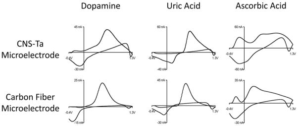
Detection of 1 μM dopamine, 20 μM uric acid, and 200 μM ascorbic acid at both CNS-Ta microelectrode (top) and cylindrical carbon fiber microelectrode (bottom).
Microelectrodes are typically used in biological experiments for hours at a time to measure neurotransmission.36–39 The stability of CNS-Ta wire microelectrodes was investigated by continuously applying the potential waveform to the microelectrode for an extended period of time and injecting a bolus of dopamine every 2 hours. Over a 10 hour period, the relative standard deviation (RSD) at the same electrode was 3.7% ± 0.8% (n=4), as shown in figure 8A. The stability of these CNS-Ta microelectrodes over ten days was tested every two days, as shown in Figure 8B. The RSD at the same electrode over ten days was 6.3% ± 0.3% (n=5). The small value of RSD at the same electrode over time and low SEM among different electrodes indicates high stability and high reproducibility of CNS-Ta microelectrodes. The promising selectivity and the stability of CNS-Ta microelectrodes demonstrate that these microelectrodes could be suitable for future in vivo studies.
Figure 8.

Stability Study. The response of a CNS-Ta electrode to 1 μM dopamine was tested (A) every 2 hours for 10 hours at four electrodes and (B) every 2 day over a 10 day duration (n=5 each). The electrodes were scanned from −0.4 V to 1.0 V at 400 V/sec at 10 Hz. Error bars represents standard error of mean.
Discussion
Enhanced current for dopamine at the carbon nanospike-modified microelectrodes is likely due to the increased edge plane carbon and carbon-oxygen functional groups on the surface.22 The optimized CNS structure is a thin layer, aligned carbon with many defects, which is good for detection of adsorption-controlled species. Growing carbon nanospikes with PECVD causes an edge plane carbon rich surface as all the D/G ratios are greater than one.9 However, as shown by the Raman spectra in Figure 2, the sensitivity did not directly follow D/G ratios. The CNS-Ta electrodes had a slightly lower D/G ratio and the highest dopamine current, similar to that of CNS-Pd electrodes which had the highest D/G ratios. Dangling bonds at edge-plane carbon and surface oxide groups provide sites for adsorption of dopamine; thus, the surface oxide groups may play an important role in adsorption than just the number of dangling bonds.27 The carbon is functionalized when the waveform is applied to the electrode during the experiment.22 The optimal waveform used for dopamine detection at CNS-metal microelectrodes was scanning to 1.3 V, which has been shown to oxidize the surface of CFMEs and break carbon-carbon bonds, improving the sensitivity for dopamine detection.22 The waveform was applied to electrodes for 30 min before use to allow electrodes to equilibrate and have stable background currents, as changes in background current were observed initially due to surface changes. Etching the carbon nanomaterial would increase the sites for dopamine adsorption and create a more sensitive electrode material.26
The growth of carbon nanospikes on metal wires is advantageous because it provides uniform surface coverage over the entire metal and does not require the deposition of a catalyst, a necessary but challenging step in most carbon nanomaterial growth. Uniform catalyst coating of a cylindrical microelectrode is especially difficult since many of the methods are directional, such as e-beam deposition of catalysts.40 Moreover, a buffer layer is usually applied between the catalyst and the substrate to enhance growth efficiency by limiting the diffusion of the catalyst into the substrate upon heating. This insulating buffer layer might cause heterogeneous electron transfer and narrow the potential window.41 The catalyst-free method of CNS growth provides an aligned carbon nanomaterial that covers an entire cylinder and has good electrical contact between CNS and metallic substrate. Dozens of electrodes can be made at once with high reproducibility. In comparison to CFMEs, CNS-Ta microelectrodes with optimized growth conditions have comparable sensitivity per unit area, enhanced selectivity, faster electron transfer kinetics (ΔEP), more reversible oxidation for dopamine, and promising stability. These properties, particularly the lower ΔEp and increased reversibility, are similar to microelectrodes made from CNT yarns and fibers.6,30,42
Comparisons of carbon nanospike-coated metal electrodes to other carbon nanomaterial electrodes are shown in Table 2. This table presents data from studies using FSCV for the detection of dopamine, since that is the easiest data to compare. CNS coated Ta microelectrodes exhibit relatively high sensitivity to dopamine, in the same range as the most sensitive methods of oPPY-CNT coated CFMEs, Nafion-CNT coated CFMEs and PEI-CNT fiber microelectrodes. All three of those sensitive methods required a polymer in addition to CNTs, which can affect the time response, and the CNS method has similar sensitivity without requiring a polymer. The ΔEp for CNS-Ta microelectrodes is similar to other carbon nanomaterial electrodes where a substrate was coated with carbon nanomaterial. Only CNT yarn electrodes, made of pure CNTs, have a substantially better ΔEp. Comparisons to other nanomaterial studies where traditional electrochemistry methods have been used are more difficult. CNS-Ta microelectrodes have a significantly better LOD (8 ± 2nM with FSCV compared to 0.17 μM with differential pulse voltammetry) than multilayered graphene nanoflake electrodes, which were also catalyst free. However, since the scan rate applied in this work is several magnitude faster than conventional slow-scan cyclic voltammetry which has significant effect on ΔEP and charging current, the electron transfer kinetics and capacitance are not comparable.
Table 2.
Comparison of LOD and ΔEp for FSCV measurements at carbon nanomaterial electrodes.
| Microelectrode | LOD/nM | ΔEP/V | Reference |
|---|---|---|---|
| CONH2-CNT/CFME | 130 | 0.52 ± 0.05 | 31 |
| COOH-CNT/CFME | 180 | 0.55 ± 0.08 | 31 |
| Carbon nanofiber electrode | 500* | N/A | 13 |
| oPPY-CNT/CFME | 3.7 ± 0.5 | N/A | 43 |
| Nafion-CNT/CFME | 4 ± 1 | N/A | 43 |
| SWCNT forest/CFME | 17 ± 3 | 0.67 ± 0.01 | 44 |
| CNT Yarn disk electrode | 13 ± 2 | 0.40 ± 0.01 | 6 |
| CNT Yarn Microelectrode | 10 ± 0.08 | 0.58 ± 0.03 | 30 |
| PEI-CNT fiber microelectrode | 4.7 ± 0.2 | 0.67 ± 0.03 | 42 |
| PVA-CNT fiber microelectrode | 53 ± 5 | 0.97 ± 0.03 | 42 |
| Carbon nanopipette electrode | 25 ± 5 | 0.52 ± 0.01 | 45 |
| CNS-Ta microelectrode** | 8 ± 2 | 0.55 ± 0.03 | This work |
LOD not available so concentration shown is the lowest dopamine concentration detected.
LOD and ΔEP obtained at CNS coated tantalum with 7.5 minutes growth duration.
N/A Not available.
Although this study has primarily focused on dopamine detection, these CNS-wire microelectrodes could be used to detect other electroactive neurochemicals or biomolecules. Electrophysiology studies often use arrays of metal wires and future experiments could investigate making arrays of the CNS-coated metal wires for multiplexed electrochemical experiments. Future experiments could also investigate the anti-fouling properties of these novel sensors and their applicability in vivo.
Conclusions
Carbon nanospikes grown on metal wires can be used as microelectrode sensors for dopamine detection. The method is advantageous for two main reasons: it provides complete surface coverage of carbon growth over the entire metal material and it does not require the deposition of a catalyst. Background charging currents change in shape and increase in magnitude upon CNS coating, indicating the surface is carbonaceous. Bare metal wires show no Faradaic peaks for low concentrations of dopamine, while CNS-coated wires can monitor low concentrations of dopamine. Limits of detection and ΔEp are lower for CNS coated wires compared with CFMEs and the signal for dopamine is more reversible. Dopamine is adsorption controlled at CNS-Ta electrodes and the currents for dopamine are stable for ten hours with continuous scanning as well as for long term test up to ten days. Moreover, CNS-Ta microelectrodes exhibited promising selectivity to dopamine, uric acid, and ascorbic acid. Thus, CNS-Ta electrodes have all the beneficial properties of carbon microelectrodes and may be a useful sensor for future applications because they are easy to batch fabricate.
Supplementary Material
Acknowledgments
This work was funded by NIH (R01 MH085159, R21DA037584). AGZ is currently supported by a NIH-NIDA T32 Training Grant DA07268. Synthesis and physical characterization of the carbon nanospikes-metal wires were conducted at the Center for Nanophase Materials Sciences, Oak Ridge National Lab, which is a DOE Office of Science User Facility (User grant CNMS2014-083).
References
- 1.Huffman ML, Venton BJ. Electroanalysis. 2008;20:2422–2428. [Google Scholar]
- 2.Heien ML, Johnson MA, Wightman RM. Anal Chem. 2004;76:5697–5704. doi: 10.1021/ac0491509. [DOI] [PubMed] [Google Scholar]
- 3.Hermans A, Wightman RM. Langmuir. 2006;22:10348–10353. doi: 10.1021/la061209e. [DOI] [PMC free article] [PubMed] [Google Scholar]
- 4.Swamy BEK, Venton BJ. Analyst. 2007;132:876–884. doi: 10.1039/b705552h. [DOI] [PubMed] [Google Scholar]
- 5.Banks CE, Compton RG. Analyst. 2006;131:15–21. doi: 10.1039/b512688f. [DOI] [PubMed] [Google Scholar]
- 6.Schmidt AC, Wang X, Zhu Y, Sombers LA. ACS Nano. 2013;7:7864–7873. doi: 10.1021/nn402857u. [DOI] [PubMed] [Google Scholar]
- 7.Shang NG, Papakonstantinou P, McMullan M, Chu M, Stamboulis A, Potenza A, Dhesi SS, Marchetto H. Adv Funct Mater. 2008;18:3506–3514. [Google Scholar]
- 8.Claussen JC, Kumar A, Jaroch DB, Khawaja MH, Hibbard AB, Porterfield DM, Fisher TS. Adv Funct Mater. 2012;22:3399–3405. [Google Scholar]
- 9.Meyyappan M. Journal of Physics D-Applied Physics. 2009;42:213001–2130016. [Google Scholar]
- 10.Matthews K, Cruden BA, Chen B, Meyyappan M, Delzeit L. J Nanosci Nanotechnol. 2002;2:475–480. doi: 10.1166/153348802760394025. [DOI] [PubMed] [Google Scholar]
- 11.Yu Z, McKnight TE, Ericson MN, Melechko AV, Simpson ML, Morrison B., III Nano Lett. 2007;7:2188–2195. doi: 10.1021/nl070291a. [DOI] [PubMed] [Google Scholar]
- 12.Yu Z, McKnight TE, Ericson MN, Melechko AV, Simpson ML, Morrison B., III Nanomedicine. 2012;8:419–423. doi: 10.1016/j.nano.2012.02.011. [DOI] [PMC free article] [PubMed] [Google Scholar]
- 13.Koehne JE, Marsh M, Boakye A, Douglas B, Kim IY, Chang SY, Jang DP, Bennet KE, Kimble C, Andrews R, Meyyappan M, Lee KH. Analyst. 2011;136:1802–1805. doi: 10.1039/c1an15025a. [DOI] [PMC free article] [PubMed] [Google Scholar]
- 14.Koehne JE, Chen H, Cassell A, Liu GY, Li J, Meyyappan M. Biomed Mater Eng. 2009;19:35–43. doi: 10.3233/BME-2009-0561. [DOI] [PubMed] [Google Scholar]
- 15.Rand E, Periyakaruppan A, Tanaka Z, Zhang DA, Marsh MP, Andrews RJ, Lee KH, Chen B, Meyyappan M, Koehne JE. Biosens Bioelectron. 2013;42:434–438. doi: 10.1016/j.bios.2012.10.080. [DOI] [PMC free article] [PubMed] [Google Scholar]
- 16.Zhang DA, Rand E, Marsh M, Andrews RJ, Lee KH, Meyyappan M, Koehne JE. Mol Neurobiol. 2013;48:380–385. doi: 10.1007/s12035-013-8531-6. [DOI] [PMC free article] [PubMed] [Google Scholar]
- 17.Srivastava SK, Shukla AK, Vankar V, Kumar V. Thin Solid Films. 2005;492:124–130. [Google Scholar]
- 18.Shang NG, Au FCK, Meng XM, Lee CS, Bello I, Lee ST. Chemical Physics Letters. 2002;358:187–191. [Google Scholar]
- 19.Ando Y, Zhao X, Ohkohchi M. Carbon. 1997;35:153–158. [Google Scholar]
- 20.Sheridan LB, Hensley DK, Lavrik NV, Smith SC, Schwartz V, Liang C, Wu Z, Meyer HM, Rondinone AJ. J Electrochem Soc. 2014;161:H558–H563. [Google Scholar]
- 21.Talapatra S, Kar S, Pal SK, Vajtai R, Ci L, Victor P, Shaijumon MM, Kaur S, Nalamasu O, Ajayan PM. Nature Nanotech. 2006;1:112–116. doi: 10.1038/nnano.2006.56. [DOI] [PubMed] [Google Scholar]
- 22.Heien MLAV, Phillips PEM, Stuber GD, Seipel AT, Wightman RM. Analyst. 2003;128:1413–1419. doi: 10.1039/b307024g. [DOI] [PubMed] [Google Scholar]
- 23.Zestos AG, Nguyen MD, Poe BL, Jacobs CB, Venton BJ. Sensors and Actuators B-Chemical. 2013;182:652–658. doi: 10.1016/j.snb.2013.03.066. [DOI] [PMC free article] [PubMed] [Google Scholar]
- 24.Rand E, Periyakaruppan A, Tanaka Z, Zhang DA, Marsh MP, Andrews RJ, Lee KH, Chen B, Meyyappan M, Koehne JE. Biosens bioelectron. 2013;42:434–438. doi: 10.1016/j.bios.2012.10.080. [DOI] [PMC free article] [PubMed] [Google Scholar]
- 25.Bhuvana T, Kumar A, Sood A, Gerzeski RH, Hu J, Bhadram VS, Narayana C, Fisher TS. ACS Appl Mater Interfaces. 2010;2:644–648. doi: 10.1021/am9009154. [DOI] [PubMed] [Google Scholar]
- 26.Takmakov P, Zachek MK, Keithley RB, Walsh PL, Donley C, McCarty GS, Wightman RM. Anal Chem. 2010;82:2020–2028. doi: 10.1021/ac902753x. [DOI] [PMC free article] [PubMed] [Google Scholar]
- 27.Roberts JG, Moody BP, McCarty GS, Sombers LA. Langmuir. 2010;26:9116–9122. doi: 10.1021/la9048924. [DOI] [PubMed] [Google Scholar]
- 28.Electrical Conductivities of Materials. Vol. 2. Virginia Beach, VA: Eddy Current Technology Incorporated; 2002. [Google Scholar]
- 29.Long JT, Weber SG. Anal Chem. 1988;60:2309–2311. doi: 10.1021/ac00166a002. [DOI] [PubMed] [Google Scholar]
- 30.Jacobs CB, Ivanov IN, Nguyen MD, Zestos AG, Venton BJ. Anal Chem. 2014;86:5721–5727. doi: 10.1021/ac404050t. [DOI] [PMC free article] [PubMed] [Google Scholar]
- 31.Jacobs CB, Vickrey TL, Venton BJ. Analyst. 2011;136:3557–3565. doi: 10.1039/c0an00854k. [DOI] [PMC free article] [PubMed] [Google Scholar]
- 32.Bath BD, Michael DJ, Trafton BJ, Joseph JD, Runnels PL, Wightman RM. Anal Chem. 2000;72:5994–6002. doi: 10.1021/ac000849y. [DOI] [PubMed] [Google Scholar]
- 33.Pisoschi AM, Pop A, Serban AI, Fafaneata C. Electrochim Acta. 2014;121:443–460. [Google Scholar]
- 34.Brajter-Toth A, El-Nour KA, Cavalheiro ET, Bravo R. Anal Chem. 2000;72:1576–1584. doi: 10.1021/ac9906680. [DOI] [PubMed] [Google Scholar]
- 35.Yang C, Denno ME, Pyakurel P, Venton BJ. Anal Chim Acta. 2015;887:17–37. doi: 10.1016/j.aca.2015.05.049. [DOI] [PMC free article] [PubMed] [Google Scholar]
- 36.Zachek MK, Takmakov P, Park J, Wightman RM, McCarty GS. Biosensors & Bioelectronics. 2010;25:1179–1185. doi: 10.1016/j.bios.2009.10.008. [DOI] [PMC free article] [PubMed] [Google Scholar]
- 37.Phillips PEM, Wightman RM. Trac-Trends in Analytical Chemistry. 2003;22:509–514. [Google Scholar]
- 38.Williams JE, Wieczorek W, Willner P, Kruk ZL. Brain Res. 1995;678:225–232. doi: 10.1016/0006-8993(95)00188-v. [DOI] [PubMed] [Google Scholar]
- 39.Nguyen MD, Lee ST, Ross AE, Ryals M, Choudhry VI, Venton BJ. Plos One. 2014;9:e87165. doi: 10.1371/journal.pone.0087165. [DOI] [PMC free article] [PubMed] [Google Scholar]
- 40.Hart AJ, Slocum AH, Royer L. Carbon. 2006;44:348–359. [Google Scholar]
- 41.Magrez A, Seo JW, Smajda R, Mionic M, Forro L. Materials. 2010;3:4871–4891. doi: 10.3390/ma3114871. [DOI] [PMC free article] [PubMed] [Google Scholar]
- 42.Zestos AG, Jacobs CB, Trikantzopoulos E, Ross AE, Venton BJ. Anal Chem. 2014;86:8568–8575. doi: 10.1021/ac5003273. [DOI] [PMC free article] [PubMed] [Google Scholar]
- 43.Peairs MJ, Ross AE, Venton BJ. Anal Methods. 2011;3:2379–2386. [Google Scholar]
- 44.Xiao N, Venton BJ. Anal Chem. 2012;84:7816–7822. doi: 10.1021/ac301445w. [DOI] [PMC free article] [PubMed] [Google Scholar]
- 45.Rees HR, Anderson SE, Privman E, Bau HH, Venton BJ. Anal Chem. 2015;87:3849–3855. doi: 10.1021/ac504596y. [DOI] [PMC free article] [PubMed] [Google Scholar]
Associated Data
This section collects any data citations, data availability statements, or supplementary materials included in this article.