Abstract
In this letter, we propose a new method for selective imaging of surface bound probes or simultaneous imaging of surface bound plus fluorescence from dye molecules in bulk water solution. The principle of this method relies on use of two optical modes with different mode distributions, filed decay lengths and polarization states that are sustaining in a plasmon waveguide. The two modes with different decay lengths couple with dye molecules of different regions, at different distances from the PCW-water interface. The emission from two different regions occur as two coupled emission rings with different polarizations and emitting angles in the back focal plane (BFP) images. By using an electric-driven liquid crystal in BFP imaging, we selectively imaged surface or surface plus bulk fluorescence. Accordingly two coupled emissions can be switched ON or OFF independently, that are for either surface or bulk fluorescence imaging. Our work provides a new method for fluorescence imaging or sensing just by using a planar multilayer film, which may be a useful for fluorescence-based techniques in chemistry, materials science, molecular biology, and medicine.
Introduction
Fluorescence detection is an important tool in biosciences. Clinical diagnostics and DNA analysis, a few to note, frequently use fluorescence assays of surface-bound capture molecule, such as antibodies or DNA oligomers and target molecules. 1-4 Fluorescence detection and imaging depends on the location of the excitation optical field. For example, the evanescent electromagnetic field of total internal reflection (TIR) is used for surface imaging. 5, 6 In TIR measurements, the slide is illuminated with light incident at an angle above the critical angle, resulting in excitation by the evanescent field which penetrates about 100 nm into the sample that is above the glass-sample interface. This localization allows selective observation of biomolecules at surfaces, an area that is of fundamental importance to a wide spectrum of disciplines in cell and molecular biology. In other words, TIR illumination is used to selective surface imaging with minimized background signal from the bulk sample.
For surface-based assays mentioned above, the samples are typically washed to remove unbound fluorophores. However, for many types of experiments, where the experimental requirement is to measure weak-binding between a surface bound capture molecule and a target molecule in the bulk phase, the emission signal from the bulk phase of the sample may provide useful information. Also, if the affinity constants are weak the surface cannot be washed because the target will be washed away. In these cases it would be useful to selectively observe both the surface-bound and bulk phase target molecules. For surface-bound assays there have been attempts to minimize the bulk signal using methods to enhance the intensity of the surface-localized fluorophores and thereby eliminate the need for washing unbound fluorophores. 7, 8 For TIR it is difficult to obtain a wide range of evanescent wave penetration depths.9-11 which limits its ability to detect fluorophores in the bulk phase. The epi-fluorescence illumination is typically used for the wide-field or imaging the bulk phase away from the glass surface. Accordingly, either surface or bulk imaging can be achieved using TIR or epi-fluorescence imaging methods, respectively, and it is not easy to realize the two imaging methods simultaneously. Also, switching between these two imaging techniques requires precise mechanical alignment and often is beyond feasibility.
Herein, we describe a simple approach to obtain evanescent fields with different penetration depths into the sample using a plasmon-coupled waveguide (PCW). This structure consists of a metal film coated with silica with a thickness comparable to the wavelength. Specifically, our PCW consist of a glass slide coated with 45 nm of Ag, which is then coated with 280 nm of silica layer. To mimic the use of this PCW in assays and cell imaging we used Rhodamine 6G (Rh6G) localized in a PMMA layer (80 nm thickness), which is on top of the silica. The PCW is then covered with aqueous solution of Rh6G providing signal from the bulk phase. We show that amounts of surface-bound and bulk phase fluorophores can be resolved using emission coupled to the PCW. The interaction of the surface and bulk phase fluorophores with the Transverse Magnetic (TM) and Transverse Electric (TE) modes, respectively, of the PCW can be imaged using back focal plane imaging. The TM and TE modes sustained in the PCW structure have different penetration depths into the sample, have different polarizations and emission angles, and can be used to resolve the relative amounts of emission from the surface or bulk phase of the samples. Taking advantages of the polarization filtering function of an electrical-driven liquid crystal (LC) plate, the two kinds of coupled emissions can be detected independently, which allows for observing the surface and bulk phase sensing or imaging.
Experimental Methods
The schematic diagram of the experimental setup for leakage radiation microscopy (LRM) is shown in Figure 1(a).12-14 A laser beam with a wavelength of 532 nm is expanded to fill the rear aperture of an oil immersed objective (60 X, N.A. 1.42) and then excited the Rh6G doped in the PMMA layer or in water solution. The samples were placed on the front focal plane of the objective. A collection lens is used to collect the reflected laser beam and fluorescence which are then imaged onto a CCD detector. By adjusting the position of the CCD detector and the collection lens, both the direct space image and back focal plane (BFP) images are obtained. A 550 nm long-pass filter and a series of band pass filters with center wavelengths ranging from 550 to 640 (10 nm step) are used to block the excitation beam and allow the narrow band of wavelengths of fluorescence to reach the CCD detector. The bandwidths (full width at half-maximum) of the band pass filters are 10 nm. A linear polarizer is placed before the collection lens to check the polarization state of the emitting fluorescence. For selecting the polarization state of the observed fluorescence an electric-driven liquid crystal plate (RPC, ARCoptix, Switzerland) is installed before the polarizer. The LC plate and the polarizer form a group of polarization converter (shown in a dashed-line box in Figure 1 (a)) which can be removed or installed together as required. A fiber-optics probe combined with the spectrometer (ihR 550, JY) is used to replace the CCD detector and measured the fluorescence spectra. The band pass filter was removed for spectral measurements.
Figure 1.
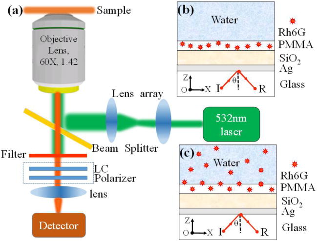
(a) Schematic diagram of LRM microscopy, LC, liquid crystal. The LC and Polarizer work as the polarization converter. Structural diagram of the sample (PCW) with no Rh6G (Sample 1, (b)) and with Rh6G (Sample 2, (c)) in the water solution.
The structural diagram of the PCW is shown in Figure 1(b) and (c). The PCW consists of a layer of SiO2 on Ag layer on glass coverslip. The SiO2 film was deposited on the Ag film by using a sputtering deposition apparatus in a vacuum. The Ag film was evaporated on a glass substrate by thermal evaporation. Dye Rh6G (10-2 M) is dissolved in the polymethylmethacrylate solution (PMMA, 950K, A2, Micro. Chem, German), which is then spin-coated onto the SiO2 film. The thicknesses of the Ag, SiO2 and PMMA films are about 45 nm, 280 nm, and 80 nm, respectively. Then a drop of water solution (with or without Rh6G molecules) is placed on the PMMA layer to mimic the liquid environment. For comparisons, two control samples are adopted. The Sample 1 (Figure 2(b)) does not have Rh6G molecules in the water solution and the Sample 2 (Figure 2 (c)) has Rh6G molecules in the water. The dye molecules doped in the PMMA layer are considered to be the surface-bound fluorophores, and the Rh6G molecules in the water solution are as the bulk phase fluorophores.
Figure 2.
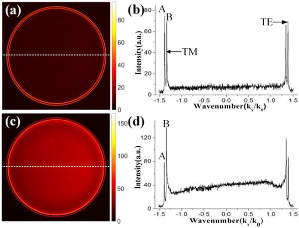
Fourier plane fluorescence image of the Sample 1 (a) and Sample 2 (c) captured by the LRM. Profiles (b) and (d) are fluorescence intensity distributions along the white dash lines indicated in FP images (a) and (c), respectively.
Results and Discussion
Figure 2 (a) shows the fluorescence intensity distribution on BFP of the objective.15,16 The center wavelength of the band pass filter is 600 nm. Here the fluorescence is emitted from the Rh6G molecules doped in the PMMA layer because the water layer does not contain Rh6G (Sample 1). Two thin bright rings appears with different diameters. As we know, the FP image represents the emitting angle of the fluorescence (or X-component wavenumber of the fluorescence), so the two rings indicate the directional emission of the fluorescence at two particular polar angles. To determine the polarization state of the coupled emission rings, a polarizer is placed before the CCD and rotated (experimental results not shown here). From the intensity distribution changes on the bright rings, we can find that fluorescence on the inner ring is polarized along the radially direction (corresponding to the TM polarization), and that on the outer ring is along the azimuthally direction (corresponding to the TE polarization). When viewed with polarization-sensitive detection the inner ring is like a donut shaped radially polarized beam and the outer ring is similar as a donut shaped azimuthally polarized beam.17
To have quantitative investigation of this coupled emission, the intensity profiles along the white dashed line on Figure 2 (a) is plotted in Figure 2 (b). The horizontal axis is the X-component wavenumber of the fluorescence which can be derived from the known N.A of the objective. The vertical axis is the fluorescence intensity. Because of symmetry around the surface normal axis there are two peaks on both sides of the intensity traces. We use the left peaks (labeled as A and B) for the following analysis. From the X-axis value of peaks A and B, we can derive the corresponding polar angle θ as about 64.42° and 61.03°, respectively (Kx/K0=n*sin (θ), n is the refractive index of the glass substrate). The normalized wavenumber (Kx/K0) is also the effective reflective index of the corresponding mode. Here we define another parameter RBA as the intensity ratio between peak B and A. From Figures 2 (a) and (b), the RBA is 0.97 which means that the directional fluorescence emission at large polar angle (at peak A) is stronger than that at smaller angle (at B). The value of RBA will be changed when the dye molecules are also present in the water solutions (Sample 2). Figures 2 (c) and (d) show the corresponding FP fluorescence image and the intensity profile. In this case, the emission angles have not been changed but the intensity ratio (RBA) changed to 1.658, which means the fluorescence at smaller polar angle become stronger as compared to that from the larger polar angle. From the color map of Figures 2 (a) and (c) we can find that the intensity of the two rings become brighter but the intensity change of the inner ring is larger than that of the outer ring. This means that more Rh6G molecules in the water solution are coupled to the inner ring than the outer ring or the coupling efficiency is higher for Rh6G molecules with the inner ring than the outer ring.
To understand the origin of the two rings shown in Figure 2, we used the transfer matrix method (TMM)18 to simulate the angle-dependent reflectivity. The used incident wavelength was 600 nm which corresponds to the emission wavelength in Figure 2. The refractive indices of the glass, Ag, SiO2, PMMA, and water are 1.52, 0.124+i3.7316, 1.46, 1.49, and 1.33 respectively. The thickness of Ag, SiO2, and PMMA are 45, 280, and 80 nm, respectively. For the TM or TE polarized incident light, there is a reflection dip at 61.02° or 64.43°, respectively (Figure 3). The polarization and resonant angle of these dips are consistent with the corresponding rings in Figure 2. So we can conclude that the inner ring is induced by the coupling with the TM mode and the outer ring is due to the TE mode.
Figure 3.
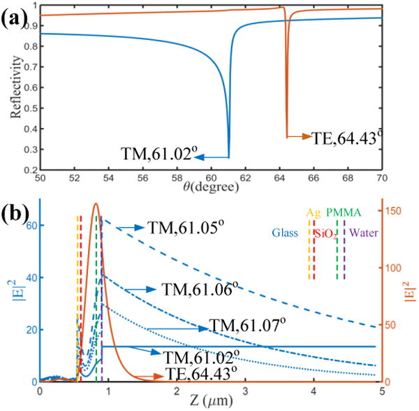
(a) Calculated angle-dependent reflectivity curves from the PCW structure shown in figure 1 (b). The incident light is TM-polarized (blue line) or TE-polarized (red line). The incident wavelength is 600 nm. (b) The electric-field intensity distributions across the PCW and sample with the incident angles fixed at the indicated angles.
Figure 3 (b) presents the electric-field intensity (E2) distribution of these two modes along the normal axis of the multilayer (Z-axis, Figure 1 (b)). For the TE mode, electric field for θ = 64.43° decays with the distance from the PMMA layer. The decay length is about 188 nm. The local electric field intensity is highly enhanced inside the PMMA and SiO2 layer. For the TM mode, when the incident angle is fixed at the reflectivity dip (θ = 61.02°), the electric field intensity inside the water solution is constant, meaning a propagating optical field. In this case, the incident angle is smaller than the total internal reflection angle (TIRA) between the water and following layers. When the incident angle is slightly increased, such as to 61.05°, 61.06°, and 61.07°, the corresponding electric field intensity distributions are confined inside the SiO2 and PMMA layer, and the filed inside the water solution is evanescent and decays with the distance from the PMMA layer. The decay lengths at the three incident angles are 3643 nm, 2108 nm, and 1632 nm, which are much longer than that of the TE mode. The long decay length of the TM mode can be analyzed from the effective index of this mode. The effective index at these incident angle is 1.52*sin (61.05°) =1.3306, which is close to the refractive index of the water solution (1.33). Then, the optical filed inside the PMMA and SiO2 layer will penetrate deeply into the water solution. On the other hand, the effective index of the TE mode is about 1.37 which is much larger than 1.33, so the decay length is much shorter. The effective indices of the two modes are smaller than the refractive index of the glass substrate, so they can be considered as leaky modes.19 For the present structure also contains a lower mode, such as zero-order TM mode (TM0). But its effective index is larger than that of the glass substrate, so it cannot be excited through the Kretschmann configuration. 20
It should be noted, the evanescent field with a long decay length is different from the field generated by the total internal reflection (TIR). As we know, the TIRA is not sensitive to the polarization of the incident light, and only when the incident angle is larger than the TIRA, the evanescent field will be generated. In our experiments, the long decay length of evanescent mode only appears in the case of TM polarized incident light. Figure 3 (b) demonstrates that the penetration depth of TM mode into the water solution is much longer than that of TE mode. Then the dye molecules in the water solution couple more with the TM mode than that with the TE mode. As a result, the intensity of the TM-polarized (inner ring) becomes stronger than that of the TE-polarized (outer ring).
Based on the above experimental and simulation results, we can judge that the fluorescence on the outer ring (TE mode) is mainly from the dye molecules doped in the PMMA layer, from the surface of the PCW. This mode can be used to collect fluorescence signal from surface bound fluorophores. On the other hand, the fluorescence on the inner ring is the emission from the dye molecules in both the PMMA film and the water solution, which can be adopted for the bulk phase measurement. Then, the selective collection of these two kinds of coupled fluorescence signals can be used to resolve the emission intensities from the surface and bulk regions of the sample. The angles of these two coupled emissions are very close, so it is not easy to select one from the two rings with a mechanical aperture or iris. However, the polarization difference between these two rings provides another means to select each ring. As described above, the inner ring is like a radially polarized beam and the outer one has azimuthally polarization. The electric driven liquid crystal plate (Figure 1 a) was used to convert a linearly polarized beam into radially or azimuthally polarized beam. Here, we use its reverse function which is to convert the radially and azimuthally polarized beams into linearly polarized beams with orthogonal polarization directions.21 The polarization direction of the converted linearly polarized beam can be tuned through the voltage (0 or 8 v) loaded on the LC plate. After the LC, a linear polarizer with fixed orientation is used as shown in Figure 1 (a) to filter the two rings and allow only one ring of emission to reach the CCD. When the voltage is 0 v, only the inner ring is observed in the BFP image. The intensity profile along the dash line on (a) also displays only one peak on each side (peak B). At this voltage, the polarization direction of the converted linearly polarized beam (from radially polarized beam) of inner ring is parallel with the orientation of the polarizer, so it can pass through this polarizer. In contrast, the outer ring (azimuthally polarization) is also converted into the linearly polarized beam but its direction is perpendicular to the orientation of the polarizer, so it is blocked. As a result, only the fluorescence signal on the inner ring reaches the CCD. When the applied voltage is 8 v, the opposite phenomenon occurs where only the outer ring appears as shown in Figures 4 (c) and (d). These experimental results demonstrate that the surface and bulk fluorescence information of the samples can be selectively measured by the voltage applied to the LC and without any mechanical adjustments.
Figure 4.
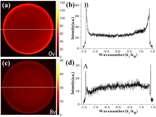
Fourier plane fluorescence images from Sample 2 with the voltage loaded on LC is 0 v (a) or 8 v (c). Profiles (b) and (d) are fluorescence intensity distribution along the white dash lines indicated in (a) and (c), respectively.
The emission spectrum of Rh6G spans a wide range of wavelengths from below 550 to 650 nm (Figure 5a). A 550 nm long pass filter is placed before the spectrometer to reject the excitation laser beam (with 532 nm wavelength). The emission spectra from Sample 2 have contributions from dye molecules in both the PMMA film and water solution. When there is no LC and polarizer before the detector, we observed a broad spectrum with peak at about 560 nm. In this case, both the TM / TE, and randomly polarized emission will reach the detector. When the LC and polarizer are used, by adjusting the voltage on the LC, we can observe the TM and TE coupled emission independently. When the voltage is 8 v, the spectrum is mainly from the TE mode and when the voltage is 0 v, the spectrum is mainly from the TM mode. Except for the intensity, the spectra taken in these three cases are similar. The emission intensity from the TM is stronger than that from the TE mode, which is consistent with the FP images shown in Figure 4. Due to the broad emission spectrum of the dye, we use a series of band-pass filters with center wavelengths ranging from 550 to 640 nm. The wavelength step is 10 nm. For Sample 1 and Sample 2, the intensity ratio between peak B and peak A (parameter RBA) at these selected wavelengths are measured and shown in Figure 5 (b). The ratios of Sample 2 are larger than the corresponding ones of Sample 1, meaning that the dye molecules in water solution are coupling more stronger to the TM modes at all these wavelengths.
Figure 5.
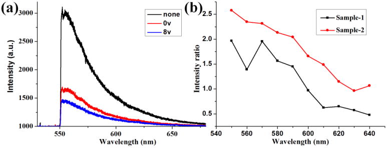
(a) Fluorescence spectra from the Sample-2 with and without the polarization converter. The voltage loaded on the LC is 0 or 8 v. (b) The intensity ratio between peak B and A on Figure 2 from Sample-1 and Sample 2. The fluorescence wavelength ranges from 550 to 640 nm selected by the band-pass filters.
Conclusion
PCWs have been used previously for fluorescence detection, but these methods were different from the present report. Surface plasmon-enhanced fluorescence (SPEF) uses the enhanced field for increased excitation intensities near the metal surface, but only the free-space emission is detected.22, 23 Surface plasmon-coupled emission (SPCE) uses both the enhanced surface-plasmon field and near-field coupling of fluorescence to the metal film. 24, 25 In SPCE the observed signal is selective for the surface-coupled emission, but does not provide a separate measurement of the bulk emission. SPCE has been reported with thick dielectric layers which support waveguide modes, but in this case the fluorophores were located throughout the dielectric and not in a region accessible to reagents and target molecules. 26, 27 The problem of separating surface and bulk phase signal also occurs in surface plasmon resonance (SPR). 28 Resolution of these two populations has been proposed using structures similar to our PCWs. 29, 30 This concept is used in the present paper but applied to fluorescence rather than changes in dielectric constants.
Taking advantages of the dual optical modes in the PCW, we determined experimentally that emission coupled into each of these modes is practically selective for surface bound or bulk phase fluorescence. The principle of this method relies on the different electric-filed (E-field) distribution and polarization state of two modes. For the TE polarized mode, its E-field localizes in the near-field of the multilayer film and so mostly the dye molecules locating near the surface of the film interact with this mode and induce the directional TE coupled emission. Additionally, by precisely selecting the thickness of the dielectric layer, decay length of the TM-polarized mode can be adjusted to be very long, even larger than the wavelength. Then, the dye molecules in this thicker region all can interact with the TM mode and result in the TM coupled emission which includes contributions from the both phases. By using an electric driven liquid crystal, the two types of coupled emissions can be switched ON or OFF independently which provides a new means for selectable surface and bulk fluorescence imaging or sensing without any mechanical alignment.
Our approach of PCW has many practical advantages. The structures do not contain any surface nanoparticle features and are readily prepared with large surface areas, without the use of costly top-down nanofabrication. The top surface is silica for which the surface chemistry is highly evolved for conjugation to biomolecules. The PCW dimensions can be adjusted for any selected wavelength, and UV and NIR wavelengths are accessible using Al and Au, respectively. In summary, PCW and its coupled emission can be readily introduced to surface-based assays and cell imaging.
Acknowledgments
This work was supported by the National Key Basic Research Program of China under grant nos. 2013CBA01703, 2012CB921900, 2015CB352003, the National Natural Science Foundation of China under grant nos. 61427818 and 11374286, 11204251. This work was also supported by NIH Grants RO1HG002655 and RO1EB006521.
Footnotes
Notes: The authors declare no competing financial interest
References
- 1.Gonzalez-Gonzalez M, Jara-Acevedo R, Matarraz S, Jara-Acevedo M, Paradinas S, Sayagues JM, Orfao A, Fuentes M. Nanotechniques in proteomics: Protein microarrays and novel detection platforms. Eur J Pharm Sciences. 2012;45:499–506. doi: 10.1016/j.ejps.2011.07.009. [DOI] [PubMed] [Google Scholar]
- 2.Hieb AR, D'Arcy S, Kramer MA, White AE, Luger K. luorescence strategies for high-throughput quantification of protein interactions. Nucleic Acids Res. 2012;40(5):1–13. doi: 10.1093/nar/gkr1045. [DOI] [PMC free article] [PubMed] [Google Scholar]
- 3.Seidel M, Niessner R. Automated analytical microarrays: a critical review. Anal Bioanal Chem. 2008;391:1521–1544. doi: 10.1007/s00216-008-2039-3. [DOI] [PMC free article] [PubMed] [Google Scholar]
- 4.Gupta PK. Single-molecule DNA sequencing technologies for future genomics research. Cell. 2008;26(11):602–61. doi: 10.1016/j.tibtech.2008.07.003. [DOI] [PubMed] [Google Scholar]
- 5.Burghardt TP, Ajtai K, Borejdo J. In situ single-molecule imaging with attoliter detection using objective total internal reflection confocal microscopy. Biochem. 2006;45:4058–4068. doi: 10.1021/bi052097d. [DOI] [PubMed] [Google Scholar]
- 6.Fiolka R, Belyaev Y, Ewers H, Stemmer A. Even illumination in total internal reflection fluorescence microscopy using laser light. Micro Res Tech. 2008;71:45–50. doi: 10.1002/jemt.20527. [DOI] [PubMed] [Google Scholar]
- 7.Szmacinski H, Badugu R, Lakowicz JR. Fabrication and characterization of planar plasmonic substrates with high fluorescence enhancement. J Phys Chem C. 2010;114:21142–21149. doi: 10.1021/jp107543v. [DOI] [PMC free article] [PubMed] [Google Scholar]
- 8.Szmacinski H, Badugu R, Mahdavi F, Blair S, Lakowicz JR. Large fluorescence enhancements of fluorophore ensembles with multilayer plasmonic substrates: Comparison of theory and experimental results. J Phys Chem C. 2012;116:21563–21571. doi: 10.1021/jp3072876. [DOI] [PMC free article] [PubMed] [Google Scholar]
- 9.Martin-Fernandez ML, Tynan CJ, Webb SED. A ‘pocket guide’ to total internal reflection fluorescence. J Microscopy. 2013;252(1):16–22. doi: 10.1111/jmi.12070. [DOI] [PMC free article] [PubMed] [Google Scholar]
- 10.Olveczky BP, Periasamy N, Verkman AS. Mapping fluorophore distributions in three dimensions by quantitative multiple angle-total internal reflection fluorescence microscopy. Biophys J. 1997;73:2836–2847. doi: 10.1016/S0006-3495(97)78312-7. [DOI] [PMC free article] [PubMed] [Google Scholar]
- 11.Zhu S, Yu AW, Hawley D, Roy R. Frustrated total internal reflection: A demonstration and review. Am J Phys. 1986;54(7):601–607. [Google Scholar]
- 12.Massenot S, Grandidier J, Bouhelier A, Colas des Francs G, Markey L, Weeber JC, Dereux A. Polymer-metal waveguides characterization by Fourier plane leakage radiation microscopy. Appl Phys Lett. 2007;91:243102. [Google Scholar]
- 13.Drezet A, Hohenau A, Koller D, Stepanov A, Ditlbacher H, Steinberger B, Aussenegg FR, Leitner A, Krenn JR. Leakage radiation microscopy of surface plasmon polaritons. Materials Science and Engineering B. 2008;149:220–229. [Google Scholar]
- 14.Zhang DG, Yuan XC, Bouhelier A. Direct image of surface-plasmon-coupled emission by leakage radiation microscopy. Appl Opt. 2010;49:875–879. doi: 10.1364/AO.49.000875. [DOI] [PubMed] [Google Scholar]
- 15.Zhang D, Badugu R, Chen Y, Yu S, Yao P, Wang P, Ming H, Lakowicz JR. Back focal plane imaging of directional emission from dye molecules coupled to one-dimensional photonic crystals. Nanotechnology. 2014;5:1–10. doi: 10.1088/0957-4484/25/14/145202. [DOI] [PMC free article] [PubMed] [Google Scholar]
- 16.Grandidier J, Colas des Francs G, Massenot S, Bouhelier A, Markey L, Weeber JC, Finot C, Dereux A. Gain-Assisted Propagation in a Plasmonic Waveguide at Telecom Wavelength. Nano Lett. 2009;9:2935–2939. doi: 10.1021/nl901314u. [DOI] [PubMed] [Google Scholar]
- 17.Zhan QW. Cylindrical vector beams: from mathematical concepts to applications. Advances in Optics and Photonics. 2008;1:1–57. [Google Scholar]
- 18.Pochi Yeh. Optical waves in layered media. Wiley Interscience. 2005 [Google Scholar]
- 19.Zia R, Selker MD, Brongersmam ML. Leaky and bound modes of surface plasmon waveguides. Phys Rev B. 2005;71:165431. [Google Scholar]
- 20.Berini P. Long-range surface plasmon polaritons. Advances in Optics and Photonics. 2009;1:484–588. [Google Scholar]
- 21.Chen YK, Zhang DG, Han L, Rui GH, Wang XX, Wang P, Ming H. Surface-plasmon-coupled emission microscopy with a polarization converter. Opt Lett. 2013;38:736–738. doi: 10.1364/OL.38.000736. [DOI] [PubMed] [Google Scholar]
- 22.Dostalek J, Knoll W. Biosensors based on surface plasmon-enhanced fluorescence spectroscopy. Biointerphases. 2008;3(3):FD12–FD22. doi: 10.1116/1.2994688. [DOI] [PubMed] [Google Scholar]
- 23.Touahir L, Tobias A, Jenkins A, Boukherroub R, Gouget-Laemmel AC, Chazalviel JN, Peretti J, Ozanam F, Szunerits S. Surface plasmon-enhanced fluorescence spectroscopy on silver based SPR substrates. J Phys Chem C. 2010;114:22582–22589. [Google Scholar]
- 24.Lakowicz JR. Radiative decay engineering 3. Surface plasmon-coupled directional emission. Anal Biochem. 2004;324:153–169. doi: 10.1016/j.ab.2003.09.039. [DOI] [PMC free article] [PubMed] [Google Scholar]
- 25.Gryczynski I, Malicka J, Gryczynski Z, Lakowicz JR. Radiative decay engineering 4. Experimental studies of surface plasmon-coupled directional emission. Anal Biochem. 2004;324:170–182. doi: 10.1016/j.ab.2003.09.036. [DOI] [PMC free article] [PubMed] [Google Scholar]
- 26.Gryczynski I, Malicka J, Nowaczyk K, Gryczynski Z, Lakowicz JR. Effects of sample thickness on the optical properties of surface plasmon-coupled emission. J Phys Chem B. 2004;108:12073–12083. doi: 10.1021/jp0312619. [DOI] [PMC free article] [PubMed] [Google Scholar]
- 27.Gryczynski I, Malicka J, Nowaczyk K, Grycyznski Z, Lakowicz JR. Waveguide-modulated surface plasmon-coupled emission of Nile blue in poly(vinyl alcohol) thin films. Thin Solid Films. 2006;510:15–20. doi: 10.1016/j.tsf.2005.07.312. [DOI] [PMC free article] [PubMed] [Google Scholar]
- 28.Homola J, editor. Surface Plasmon Resonance Based Sensors. Springer; New York: 2006. p. 251. [Google Scholar]
- 29.Bahrami F, Maisonneuve M, Meunier M, Aitchison JS, Mojahedi M. An improved refractive index sensor based on genetic optimization of plasmon waveguide resonance. Opt Exp. 2013;21(18):20863–20872. doi: 10.1364/OE.21.020863. [DOI] [PubMed] [Google Scholar]
- 30.Bahrami F, Alam MZ, Aitchison JS, Mojahedi M. Dual polarization measurements in the hybrid plasmonic biosensors. Plasmonics. 2012;8(27):423–465. [Google Scholar]


