Introduction
Fluorescence detection is a widely used technique with applications in many areas like sensing, imaging, DNA sequencing, medical diagnostics and material sciences. Although present day fluorescence technology is highly evolved, there are some natural limitations of traditional fluorescence. Fluorophores in bulk solutions emit isotropically in all directions (Figure 1A). As a result, typical detection systems collect less than 1% of the total emission.1 When fluorophores are placed on a planar surface, for example a glass slide, most of the emission occurs above the critical angle (θc) into the higher refractive index medium (Figure 1B).2 A complete collection of the emitted light requires bulky external optics that limits spatial resolution. To meet the demands of modern fluorescence formats and device miniaturization, it is important to control emission directionality and develop efficient techniques for routing and collecting the emitted light.
Figure 1.
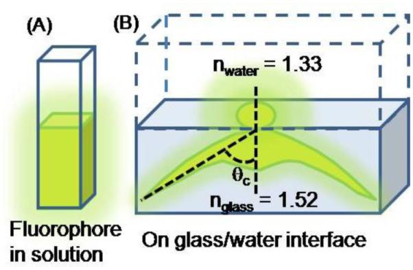
Emission patterns in solution and glass/water interface.
Apart from improving collection efficiency, controlled emission directionality has other practical implications. By converting to directional emission, fluorescence can be endowed with direction-specific information useful for multiplexing. Moreover, directional emission is valuable for effectively communicating light in optical sensors, displays and light emitting devices (LEDs).
For transforming naturally occurring isotropic emission into directional emission, it is necessary to look beyond the realm of traditional fluorescence. This opportunity is provided by the recent spectacular advances in plasmonic nanostructures and dielectric photonic crystals that enable molding of optical energy in nanoscale dimensions.3-5 Over the past couple of years, many laboratories, including ours have demonstrated numerous benefits of coupling fluorescence with metal nanostructures, thin metal films, photonic crystals and hybrid plasmonic–photonic structures.1,6-12 Instead of considering only freely propagating radiation, it is possible to utilize near–field interactions for bringing about extraordinary changes in emission properties that cannot be envisaged with classical fluorescence. The control over emission directionality essentially revolves around the targeted coupling of emission to select optical modes in the plasmonic/photonic substrate, with specific out-coupling characteristics.6,12 While plasmonic substrates modify fluorescence properties due to strong local field enhancements and surface–plasmon oscillations, photonic crystals influence fluorescence properties due to photonic band structure effects.6,12
Our efforts in tailoring fluorescence directionality have mainly been focused on the use of planar metallic and/or dielectric structures that can be prepared easily using existing thin film technologies. This Account summarizes our studies with metal–dielectric layered substrates,1,7,13-15 1–dimensional photonic crystals (1DPC),6,16 and hybrid plasmonic–photonic structures.17-19 Reflectivity simulations and dispersion diagrams are provided for understanding the different optical modes that determine the spatial distribution of coupled emission. Representative studies by other groups, based on an alternative approach using specially fabricated optical nanoantennas, is also discussed.9,10,20,21
Metal–Dielectric Layered Structures
Metal–Dielectric (MD) Substrates with Thin Dielectric Layer
When a thin metal film is illuminated with light through a high refractive index medium, like glass prism, a wavelength–dependent dip in reflectivity can be observed at a speci?c angle, θSP,λ, due to creation of surface–plasmons (Figure 2 and Supporting Information).6 The surface–plasmon waves propagate along the metal/dielectric interface due to resonant interaction between surface–charge oscillations in the metal and electromagnetic field of light. In contrast to the propagating nature of surface–plasmons along the surface, the field perpendicular to the surface is evanescent. These unique optical properties make surface–plasmons attractive for many applications; one of the most exciting prospects being their ability to concentrate and guide the flow of light.
Figure 2.
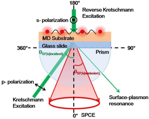
Schematic of illumination geometries, polarizations and angle notations.
Just as an incident beam couples with surface–plasmons at θSP,λ(incident), light emitted from excited fluorophores present adjacent to a metal film (within 20–250 nm), can also create surface–plasmons due to near–field interactions. The surface–plasmons induced by excited fluorophores subsequently radiate into the substrate at an angle, θSP,λ(emission), determined by the resonance condition for the emission wavelength. This remarkable phenomenon, called surface–plasmon–coupled emission (SPCE), effectively transforms omnidirectional fluorescence to sharply directional emission, distributed at two angles around the surface normal.1 Our studies have shown that SPCE is independent of the mode of excitation. Similar directional emission is observed from fluorophores excited either via the evanescent surface–plasmon field by light incident through a prism (Kretschmann configuration) or directly excited from air (Reverse Kretschmann configuration).1,6,7 Moreover, different metals (Ag, Au, Al etc) can be used to access the entire spectral range from UV to IR.7,22,23 The experimental configuration, illumination geometries and angle notations for SPCE are illustrated in Figure 2.
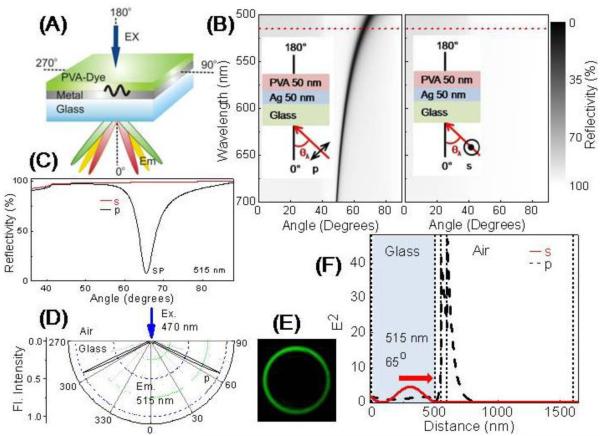
The wavelength–specific directional SPCE obtained from fluorophores contained in a dielectric medium above a thin metal film (deposited on glass slide) is depicted schematically in Figure 3A. The thickness of the dielectric layer in the metal–dielectric (MD) substrate is much lower than the emission wavelength. Excitation is in the Reverse Kretschmann configuration.
Figure 3.
(A) General schematic of SPCE. (B) Calculated R(λ,θ) plots, (C) calculated angle–dependent reflectivity at 515 nm, (D) experimental emission patterns from fluorescein, (E) projected image of SPCE from fluorescein and (F) calculated electric field intensitiy; for substrate shown in inset of (B).
The calculated reflectivity dispersion plots, R(λ,θ), for a representative metal-dielectric substrate: Ag (50 nm) and poly(vinyl alcohol) (PVA, 50 nm), is shown in Figure 3B. The dark shades signify a decrease in reflectivity and indicate creation of surface–plasmons at the corresponding wavelength and angle (see Supporting Information). The blue–shift in the resonance wavelength at increasing angles from the surface normal originates from wavelength–dependent optical properties of Ag. Reflectivity dips are present exclusively for p–polarized light; no surface–plasmon mode exists for s–polarization. The wavelength of interest, 515 nm, which is the emission maximum of the commonly used fluorophore, fluorescein, is indicated by a horizontal line.
Since SPCE is the reverse process of surface–plasmon excitation, the R(λ,θ) plots essentially provide a complete picture of the wavelength–dependent directional emission expected from fluorophores coupled to the metal-dielectric substrate. The occurrence of surface–plasmon resonance exclusively for p–polarized light implies that SPCE will be p–polarized irrespective of the nature of fluorophores or their orientation. It can be seen from the R(λ,θ) plots that for 515 nm, surface–plasmon resonance occurs at an incidence angle of 65°. This is also apparent from the angle–dependent reflectivity plot for 515 nm, Figure 3C. Accordingly, when fluorescein molecules (emission maximum 515 nm) are coupled to this substrate, sharp directional p–polarized emission is observed at 65° (and 295° due to symmetry) (Figure 3D). The real color photograph of the image formed by projecting the cone of emission from fluorescein, on a screen, shows a sharp circular image of fluorescence (Figure 3E).
Figure 3F shows simulated electric field intensity distribution (E2) for p–polarized, 515 nm light incident on the Ag-PVA substrate at 65°. The evanescent nature of the field at the metal/dielectric interface is characteristic of the surface–plasmon mode. It is easy to comprehend that emission from excited fluorescein molecules present in the same region as the evanescent field, can readily couple with surface–plasmons and radiate with plasmon–like properties. Although emission arises from fluorophores, the directionality and polarization are those of plasmons.
A variety of studies based on directional SPCE have been carried out by many groups including ours, and a number of applications have been suggested.24 SPCE offers several advantages for immunoassays,6 DNA sensing,25 conformational–switching aptamers26 and design of optical array biochips.27 SPCE has been used to image muscle fibrils and SPCE rings have been observed using leakage radiation microscopy.28,29 Another approach to using SPCE has been to take advantage of the intrinsic angular shifts for different wavelengths, to selectively identify a particular emitting species by collecting light propagating in the appropriate direction.30
Metal-Dielectric (MD) Substrates with Thick Dielectric Layer
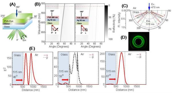
SPCE with metal-dielectric substrates having dielectric thickness much lower than the emission wavelength represents the simplest example of coupling fluorophores to metal surfaces. When the dielectric thickness becomes comparable to emission wavelength other optical modes in addition to surface–plasmons can be excited in the substrate.31 Therefore, a single emission wavelength can radiate at several angles with different polarizations, according to the resonance condition for each optical mode (Figure 4A).
Figure 4.
(A) Schematic of coupled emission in MD substrates with thick dielectric film. (B) Calculated R(λ,θ) plots, (C) experimental emission pattern from fluorescein, (D) projected image of coupled emission from fluorescein and (E) calculated electric field intensities; for substrate shown in inset of (B).
The R(λ,θ) plots for an Ag–PVA metal-dielectric substrate with Ag and PVA thickness of 50 and 380 nm, respectively, (Ag50-PVA380) are shown in Figure 4B. In this case, reflectivity dips are observed for s–polarized incident light as well. For 515 nm light, the reflectivity dip for p–polarization appears at 58°, while for s–polarization, dips are observed at 46° and 67°. Accordingly, the experimentally observed emission pattern of fluorescein coupled to this substrate shows directional emission at three angles, 46°, 58° and 67° (also 314°, 302° and 293°) with alternate polarizations (Figure 4C). The image formed by projecting this coupled fluorescence shows three circles of emission (Figure 4D).
The simulated electric field intensities of the optical modes for 515 nm light in Ag50-PVA380 substrate at the respective resonance positions (46°, 58°, 67°), are presented in Figure 4E. The intensity profile for p–polarized light (58°) shows some resemblance to the surface–plasmon mode while for the others (46°, 67°) it resembles waveguide modes. The emission observed from fluorophores coupled to metal-dielectric substrates with thick dielectric layers is thus referred as waveguide–coupled emission. Theoretical models have been developed to account for the existence of various optical modes and to predict the occurrence of directional emission at multiple angles.32 We have observed that the nature and number of optical modes supported by the MD substrate depends on thickness of the dielectric layer. Consequently, directionality of waveguide–coupled emission can be readily controlled by changing dielectric thickness.31
Although coupling of emission with multiple optical modes implies that fluorescence is not channelized into one direction, the appearance of directional emission at multiple angles and with different polarizations provides interesting options for smart solid–state lighting and optical signage. In a recent study, we have shown that metal-dielectric substrates can transform unpolarized emission from luminescent Eu(III) ions to polarized emission, with the three emission bands of Eu(III) selectively radiating in different directions.33
Metal–Dielectric–Metal (MDM) Substrates
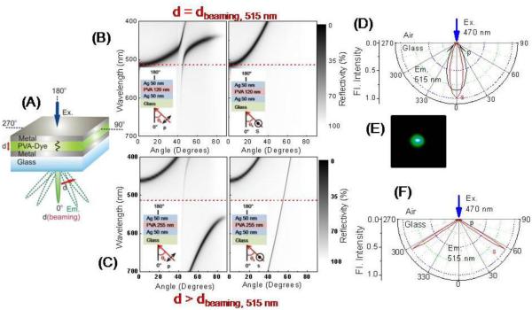
Directional emission in metal-dielectric substrates typically occurs at angles away from the surface normal, which is unsuitable for high throughput, array–based applications. It would be more advantageous to obtain the emission as a single beam close to the surface normal. With this perspective, we studied effects of an additional metal layer above the dielectric surface of the metal-dielectric substrates discussed in the previous section, leading to a metal–dielectric–metal (MDM) structure. We observed that depending on the emission wavelength, at certain thicknesses of the dielectric medium, coupling of fluorescence to Fabry–Pérot–like modes leads to beaming emission perpendicular to the substrate (see Supporting Information).13-15 The emission direction can be altered by changing the thickness of the dielectric layer containing the fluorophores (Figure 5A).
Figure 5.
(A) Schematic of coupled emission in MDM substrates. (B and C) Calculated R(λ,θ) plots. (D) Experimental emission pattern from fluorescein and (E) projected image of coupled emission from fluorescein; for substrate shown in inset of (B). (F) Experimental emission pattern from fluorescein for substrate shown in inset of (C).
The R(λ,θ) plots for two metal–dielectric–metal substrates, Ag–PVA–Ag, having different dielectric thicknesses are shown in Figures 5B and 5C; the emission maximum of fluorescein, 515 nm, is indicated by horizontal line.
For PVA thickness of 120 nm (Figure 5B), the dispersion plots show hyperbolic dark curves intersecting the Y-axis at 515 nm for both s– and p–polarized light.15 Intersection with the Y–axis at 515 nm indicates that reflectivity dip for this wavelength occurs at 0°. This is the thickness where resonance condition of Fabry–Pérot–like mode is satisfied (dbeaming, 515nm). Concurrent with the R(λ,θ) plots (Figure 5B), the angular emission pattern observed for fluorescein in Ag–PVA(120 nm)-Ag substrate, shows most of the emission in a direction normal to the substrate surface (Figure 5D) and the projected image shows a single fluorescence spot (Figure 5E).
When the dielectric thickness is different from dbeaming, 515nm, for example, at PVA thickness of 255 nm, the observed emission pattern from fluorescein shows directional emission at angles away from the surface normal (Figure 5F). It may be noted, however, that at this PVA thickness, the hyperbolic reflectivity curves in the R(λ,θ) plot intersect the Y-axis at 460 nm (Figure 5C). So it is expected that Ag–PVA(255 nm)–Ag substrates would provide beaming emission from fluorophores emitting at 460 nm.
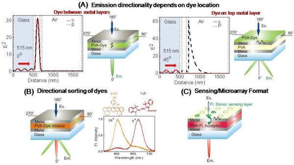
Figure 6 shows some interesting features and suggested applications of MDM–assisted fluorescence. Emission directionality from fluorophores can be tailored, based on their location in different regions of the metal–dielectric–metal substrate. As seen in Figure 6A, the electric field intensity for 515 nm light at normal incidence is localized in the dielectric layer between metal films. So fluorophores emitting at 515 nm and located in this region couple efficiently with this optical cavity mode and give rise to beaming emission at 0° (cavity mode–coupled emission). On the other hand, electric field intensity for light incident at 45° is localized at the metal-air interface (surface–plasmon mode). So fluorophores located above the top metal, couple preferentially with the surface–plasmon mode giving rise to SPCE at 45°.15
Figure 6.
(A) Schematic of dye location–dependent directional emission in MDM substrates and corresponding electric field intensity simulations for different optical modes. (B) Wavelength–dependent directional emission and directional sorting of a mixture of dyes, S101 and Cy5 in MDM substrates.13 (C) Proposed format for biosensing based on surface–plasmon energy transfer.
The dispersive features of the cavity mode can be useful for directional fluorescence sensing of multiple probes (Figure 6B). Using Ag–PVA–Ag substrate having appropriate PVA thickness, the fluorescence from two different dyes (Cy5 and S101) can be resolved by recording the emission at different angles.13 We have also shown that the nature of the metallic layer (Au, Ag, Al) and the composition of the metal–dielectric–metal substrate (mixed metal layers) can be chosen to tune the color, polarization and angular divergence of the emitted light at select observation angles.14,15
Another prospect for metal–dielectric–metal substrates is their adaptability for bioassays and microarrays. A proposed design concept is shown in Figure 6C. The top metal layer contains biomarkers capable of attaching specific fluorescence–donor labeled biomolecules. The dielectric layer between the metals contains the fluorescence–acceptor. Under suitable binding conditions, surface–plasmon–mediated energy transfer from donors on the top layer to the embedded acceptors will lead to creation of beaming emission and will allow molecule–specific biosensing with a high degree of spatial control. As proof-of-concept we have demonstrated that excitation of the donor, tris-(8-hydroxyquinoline) aluminum, coated on the top Ag layer, leads to beaming emission from the acceptor, rhodamine6G, embedded inside an Ag–PVA–Ag substrate.13
Plasmonic Optical Antennas
Other than large–area planar metal–dielectric substrates discussed above, another promising approach for generating directional emission is through plasmonic optical antennas. Optical antennas are counterparts of conventional radio and microwave antennas, operating in the visible regime that can reversibly convert propagating optical energy into localized energy in nanoscale volumes. The characteristic dimensions of nanometallic optical antennas are of the order of radiation wavelength, which makes them amenable for on–chip integration in miniature photonic applications. Although challenging to fabricate, modern nanofabrication tools like, focused ion beam milling or electron beam lithography, make this length scale increasingly accessible. A variety of antenna configurations, such as, Yagi–Uda,10 bull’s–eye,9 gratings,21 patch antennas34 and lattice antennas20 have been investigated, some of which are described below.
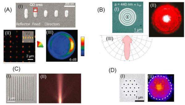
A Yagi–Uda antenna consists of an actively driven feed element surrounded by reflectors and directors. Curto et al. have demonstrated that non-directional luminescence from a single quantum dot that is precisely placed at the resonant feed element of a Yagi–Uda antenna, can be transformed into highly directional emission by near–field interactions.10 The emission directionality can be controlled by tuning the antenna dimensions (Figure 7A).
Figure 7.
(A) SEM image of Yagi-Uda antenna (I), scanning confocal image of quantum dot emission (II), and corresponding intensity distribution at the back focal plane of an objective (III). Adapted from ref. 10 with permission from AAAS. (B) SEM image of BE antenna (I), back focal plane image of coupled emission from Alexa647 (II), and corresponding angular radiation pattern (III). Adapted with permission from ref. 9. Copyright {2011} American Chemical Society. (C) SEM image of slit antenna with side grooves (I), and scanning confocal image of quantum dot emission. Adapted from ref. 20 by permission from Macmillan Publishers, Copyright (2011). (D) SEM image of plasmonic lattice antenna (I), and back focal plane image of emission from Alexa647. Adapted with permission from ref. 21. Copyright {2013} American Chemical Society.
Contrary to Yagi–Uda antennas that work for individual emitters fixed on the substrate, bull’s–eye structures consisting of concentric grooves engraved on the surface of a metallic film around a subwavelength aperture can provide unidirectional emission from fluorophores in solution (Figure 7B). The strong directionality arises due to constructive or destructive interferences between the fluorescence emitted from the aperture and the re–radiated surface–plasmon–coupled emission.9 In another variation of the bull’s–eye structure, Jun et al. have reported beaming emission from quantum dots placed in a plasmonic nanoslit coupled to a linear grating (Figure 7C). The emission wavelength and intensity could be tuned by applying an electric field across the slit.21 Recently Li et al. have also demonstrated active steering of fluorescence beams via a voltage signal in plasmonic nanoantennas coated with a luminescent layer and a liquid crystal cell as modulator.35 Off–axis beams have been generated with anisotropic grating structures and spiral plasmonic antennas.36,37 In another study, Langguth et al. have reported directional emission from hexagonal arrays of nanoapertures milled in gold film, due to plasmonic band structure effects (Figure 7D).20 The aperture arrays are technically simpler to fabricate and lend themselves to large scale replication via template stripping or imprint techniques.
Dielectric Substrates: 1-Dimensional Photonic Crystals (1DPCs)
Photonic crystals are periodic dielectric structures in one, two or three dimensions, and display photonic band gaps (PBGs), which are optical frequencies that cannot propagate in the photonic crystal structure.5 Since the pioneering work by Yablonovitch, control of light emission has been indicated as one of the most promising applications of photonic crystals.
1-Dimensional photonic crystals (1DPCs or Bragg gratings), consisting of multiple layers of dielectrics with alternating low and high dielectric constants, display a partial PBG.38 1DPCs can support surface states called Bloch surface waves (BSWs), which may be considered as dielectric analogues of surface–plasmons that propagate on a metal-dielectric surface.5,39
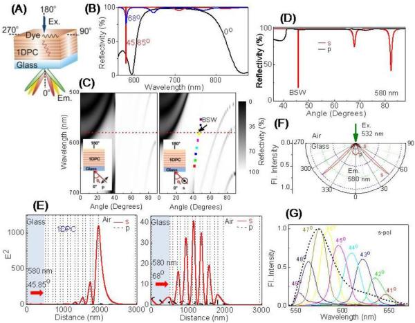
Akin to metal-dielectric structures, fluorophores can undergo near–field interactions with BSWs or other internal optical modes present in the 1DPCs, to generate directional emission (Figure 8A).12,16 In contrast to metals that are lossy, dielectrics dissipate less energy and allow sharper resonances. The 1DPC described here is composed of alternating layers of Si3N4 (H) and SiO2 (L) in the form: H(78 nm)7L(126 nm)6L(152 nm)PVA(45 nm). The fluorophores, rhodamineB, are incorporated in the PVA layer.
Figure 8.
(A) Schematic of coupled emission in 1DPC. (B) Wavelength–dependent reflectivity showing photonic band gap at normal incidence (0°) and reflectivity dips at 45.85° and 68°. (C) Calculated R(λ,θ) plots, arrow indicates sharp BSW mode. (D) Angle–dependent reflectivity at 580 nm. (E) Electric field intensity simulations for BSW and internal modes. (F) Experimental angular emission patterns from rhodamineB in 1DPC. (G) Angle–dependent spectral shifts of rhodamineB coupled to 1DPC, free–space rhodamineB emission is shown with dotted lines.12
The simulated angle–dependent reflectivity spectra for the above 1DPC structure (Figure 8B) shows a PBG from 600-850 nm, for light incident normal to the substrate. However, sharp reflectivity dips at 580 nm (emission maximum of rhodamineB) are seen for incidence angles, 45.85° and 68° due to excitation of optical modes in the 1DPC. The R(λ,θ) plot for this substrate is shown in Figure 8C. For emphasis, the reflectivity plot for 580 nm is shown separately (Figure 8D). The very sharp s–polarized resonance at 45.85° is due to the creation of BSW, as confirmed by its location on the surface of the 1DPC in the corresponding E2 profile (Figure 8E). The emission that arises due to coupling with this optical mode is called BSW–coupled emission and corresponds to the directional s–polarized intensities around 45° (and 315°) in the experimental angular emission pattern of rhodamineB (Figure 8F). The weaker emission intensities at other angles arise due to coupling with internal modes; a representative E2 profile for light incident at 68° is presented in Figure 8E.
An interesting outcome of the very sharp BSW resonance and its characteristic dispersion, is a remarkable angle–dependent change in the rhodamineB spectra (Figure 8G). The free–space emission spectrum of rhodamineB is broad (550-670 nm). The BSW–coupled emission of rhodamineB, however, is quite narrow and shifts toward shorter wavelengths with increasing angles from the surface normal.12 For better understanding, the experimentally observed emission maxima of the BSW–coupled emission of rhodamineB, at different angles, are superimposed on the BSW mode profile in the R(λ,θ) plot (Figure 8C). Further research is needed to determine if the total emission spectrum of rhodamineB is modified or if the narrowing is only due to dispersion of the 1DPC.
Although, there have been relatively few studies, so far, on modification of fluorescence with photonic crystals, these structures are an interesting alternative to the all–plasmonic approach.40-42 Recently, Angelini et al. have fabricated grating structures on 1DPCs, in analogy to plasmonic bull’s–eye structures, to obtain more control over emission directionality.43 It is expected that future methodologies will take advantage of 1DPC–assisted directional and wavelength–resolved emission for developing novel near–field fluorescence techniques.
Hybrid Plasmonic–Photonic Structures
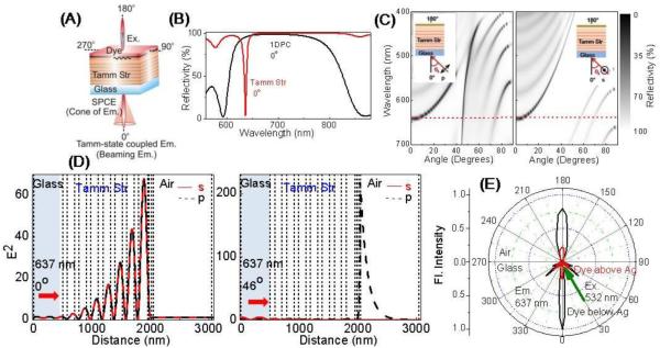
Very recently, interest has emerged in the interplay between plasmonic and photonic approaches to control flow of optical energy. We have investigated interaction of fluorescence with hybrid plasmonic–photonic structures composed of a thin Ag film on top of a 1DPC.17 Interestingly, fluorophores placed on this simple multilayer structure provide emission normal to the substrate surface, on both the glass and air side, with narrow angular distribution (Figure 9A). This effect arises due to coupling of emission with Tamm–states.
Figure 9.
(A) Schematic of coupled emission in Tamm structure. (B) Wavelength–dependent reflectivity dip in the Tamm structure vis-a-vis a 1DPC structure. (C) Calculated R(λ,θ) plots. (D) Electric field intensity simulations for Tamm–plasmon and surface–plasmon modes. (E) Experimental emission patterns in Tamm structure from nile blue located above (red line) and below (black line) the Ag layer.18
Tamm–states were first reported by Igor Tamm in 1933 for electrons at crystal boundaries.44 These states can exist between two adjacent 1DPCs with overlapping PBG.45 Knowledge of Tamm-states between a 1DPC and a metal film, known as Tamm–plasmons, is relatively new and was reported in 2007.46 The electric fields for the Tamm–plasmons are localized in the dielectric below the metal film. Unlike surface–plasmons, Tamm–plasmons can be created with s– or p–polarized light and the in plane wavevector can be zero. Moreover, the wavevector of Tamm–plasmons is smaller than that of light in vacuum, so it can be directly excited from air without the aid of prisms or gratings.17,18
The composition of the Tamm structure in this study is similar to the 1DPC discussed above but with an additional Ag layer, that is, H(78 nm)7L(126 nm)6L(152 nm)PVA(27 nm)Ag(42 nm)PVA(27 nm). The PVA layers are included to incorporate fluorophores. Addition of an Ag layer to the 1DPC structure leads to a dip in reflectivity in the PBG region, due to excitation of Tamm–plasmons (Figure 9B). The R(λ,θ) for the Tamm structure shows existence of several optical modes (Figure 9C). The Tamm resonances are seen at 0° (and 180°, figure not shown), where the hyperbolic dark curves intersect the Y–axis. The wavelength of interest, 637 nm, (emission maximum of nile blue) is marked by a horizontal line.
In accordance with reflectivity simulations, the experimental angular emission pattern from nile blue shows Tamm–state–coupled emission at 0° and 180°.18 The emission at other angles is due to coupling with additional optical modes present in the substrate. Representative electric field intensity profiles for two selected modes are shown in Figure 9D. For 637 nm light incident at 0° the electric field is localized just below the metal film as expected for the Tamm state. On the other hand, for 637 nm light incident at 46° the electric field is localized at the metal/air interface (surface–plasmon mode). Thus, the p–polarized intensity around 46° in the angular emission patterns can be assigned to SPCE. Due to the different positions of the electric field, the Tamm structure also allows tailoring of emission directionality based on dye location (Figure 9E). The beaming emission perpendicular to the substrate is most pronounced for fluorophores placed below the metal film. In recent studies we have shown that intensity of Tamm–state–coupled emission can be enhanced with proper thickness of the top metal film.19 These features can be quite useful for designing LEDs, where active mediums are present inside the emissive structures.
Concluding Remarks
The near–field coupling of fluorescence with spectrally overlapping optical modes in plasmonic and photonic structures provides a rational approach to collect, manipulate and direct emission from fluorophores without bulky optical components. While plasmonic nanoantennas have the advantage of a small footprint suitable for on–chip integration, planar metallic, dielectric or hybrid substrates, have the capability of directing emission from fluorophores with random position and orientation over a wide sample area. Moreover, the cost–effective and simple fabrication of the planar substrates makes them suitable for applications in several areas of technological significance. The possibility of excitation and emission perpendicular to the substrate surface, in MDM and Tamm structures, is particularly convenient for adaptation in multiwell plates, protein or DNA array applications and development of portable diagnostic devices. These structures can be useful for highly multiplexed fluorescence sensing, where directionality of the emitted light is used to discriminate between different sample regions.
Today we live in a visual age where efficient optical communications and imaging plays a major role. Controlling emission directionality with plasmonic/photonic structures provides the opportunity for designing new optical display technologies and advanced emissive devices. Highly integrated multipixel color-converting LEDs can be conceptualized where each pixel emits light along a different direction. These concepts are useful for solid–state lighting and can provide additional functionalities besides illumination. We anticipate that with further developments in nanotechnology and its integration into the science of near-field interactions, plasmonic and/or photonic structure-assisted fluorescence will pave the way for simple and robust next generation devices for biosensing, sequencing, clinical testing and optical signage.
Supplementary Material
Acknowledgements
We thank our collaborators and all co-authors of our published papers cited in the references. S.D.C acknowledges financial support from SERB Women Excellence Award Grant, SB/WEA-010/2013, and the support and encouragement from the host institute. This work was also supported by NIH Grants GM107986 and EB006521.
Biographies
Sharmistha Dutta Choudhury is a Scientific Officer at Bhabha Atomic Research Centre, Mumbai. She received her Ph. D. from Jadavpur University, Kolkata (2006) and was a visiting Fellow in Professor Lakowicz’s group (2011-2013). Her research interests include photophysics in supramolecular systems, fluorophore–plasmon interactions and control of emission directionality with metal–dielectric substrates.
Ramachandram Badugu is an Assistant Professor at the Centre for Fluorescence Spectroscopy, Department of Biochemistry and Molecular Biology, University of Maryland, Baltimore. His research interests are development of methodologies for fluorescence sensing, fluorescence signal amplification and/or directional emission using plasmonic, photonic or hybrid plasmonic–photonic structures.
Joseph R. Lakowicz is a Professor in the Department of Biochemistry and Molecular Biology, University of Maryland, Baltimore and the Director of the Centre for Fluorescence Spectroscopy. His research is focused on advancing the field of fluorescence spectroscopy, which includes development of plasmon-controlled and photonic crystal-controlled fluorescence. He is the sole author of the widely used book, Principles of Fluorescence Spectroscopy, 3rd edition.
Footnotes
Supporting Information. Description of surface-plasmon resonance, reflectivity calculations, Figures S1 and S2. This material is available free of charge via the Internet at http://pubs.acs.org.
References
- (1).Lakowicz JR. Radiative Decay Engineering 3. Surface Plasmon-Coupled Directional Emission. Anal. Biochem. 2004;324:153–169. doi: 10.1016/j.ab.2003.09.039. [DOI] [PMC free article] [PubMed] [Google Scholar]
- (2).Enderlein J, Ruckstuhl T, Seeger S. Highly Efficient Optical Detection of Surface-Generated Fluorescence. Appl. Optics. 1999;38:724–738. doi: 10.1364/ao.38.000724. [DOI] [PubMed] [Google Scholar]
- (3).Maier SA, Brongersma ML, Kik PG, Meltzer S, Requicha AAG, Atwater HA. Plasmonics-A Route to Nanoscale Optical Devices. Adv. Mater. 2001;13:1501–1505. [Google Scholar]
- (4).Schuller JA, Barnard ES, Cai W, Jun YC, White JS, Brongersma ML. Plasmonics for Extreme Light Concentration and Manipulation. Nature Materials. 2010;9:193–204. doi: 10.1038/nmat2630. [DOI] [PubMed] [Google Scholar]
- (5).Joannopoulos JD, Johnson SG, Winn JN, Meade RD. Photonic Crystals: Molding the Flow of Light. Second Princeton University Press; Princeton, NJ: 2008. [Google Scholar]
- (6).Lakowicz JR, Ray K, Chowdhury M, Szmacinski H, Fu Y, Zhang J, Nowaczyk K. Plasmon-Controlled Fluorescence: A New Paradigm in Fluorescence Spectroscopy. Analyst. 2008;133:1308–1346. doi: 10.1039/b802918k. [DOI] [PMC free article] [PubMed] [Google Scholar]
- (7).Gryczynski I, Malicka J, Gryczynski Z, Lakowicz JR. Radiative Decay Engineering 4. Experimental Studies of Surface Plasmon-Coupled Directional Emission. Anal. Biochem. 2004;324:170–182. doi: 10.1016/j.ab.2003.09.036. [DOI] [PMC free article] [PubMed] [Google Scholar]
- (8).Tam F, Goodrich GP, Johnson BR, Halas NJ. Plasmonic Enhancement of Molecular Fluorescence. Nano Lett. 2007;7:496–501. doi: 10.1021/nl062901x. [DOI] [PubMed] [Google Scholar]
- (9).Aouani H, Mahboub O, Devaux E, Rigneault H, Ebbesen TW, Wenger J. Plasmonic Antennas for Directional Sorting of Fluorescence Emission. Nano Lett. 2011;11:2400–2406. doi: 10.1021/nl200772d. [DOI] [PubMed] [Google Scholar]
- (10).Curto AG, Volpe G, Taminiau TH, Kreuzer MP, Quidant R, vanHulst NF. Unidirectional Emission of a Quantum Dot Coupled to a Nanoantenna. Science. 2010;329:930–932. doi: 10.1126/science.1191922. [DOI] [PubMed] [Google Scholar]
- (11).Ding B, Hrelescu C, Arnold N, Isic G, Klar TA. Spectral and Directional Reshaping of Fluorescence in Large Area Self-Assembled Plasmonic–Photonic Crystals. Nano Lett. 2013;13:378–386. doi: 10.1021/nl3035114. [DOI] [PubMed] [Google Scholar]
- (12).Badugu R, Nowaczyk K, Descrovi E, Lakowicz JR. Radiative Decay Engineering 6: Fluorescence on One-Dimensional Photonic Crystals. Anal. Biochem. 2013;442:83–96. doi: 10.1016/j.ab.2013.07.021. [DOI] [PMC free article] [PubMed] [Google Scholar]
- (13).Dutta Choudhury S, Badugu R, Nowaczyk K, Ray K, Lakowicz JR. Tuning Fluorescence Direction with Plasmonic Metal–Dielectric–Metal Substrates. J. Phys. Chem. Lett. 2013;4:227–232. doi: 10.1021/jz301867b. [DOI] [PMC free article] [PubMed] [Google Scholar]
- (14).Dutta Choudhury S, Badugu R, Ray K, Lakowicz JR. Steering Fluorescence Emission with Metal–Dielectric–Metal Structures of Au, Ag, and Al. J. Phys. Chem. C. 2013;117:15798–15807. doi: 10.1021/jp4051066. [DOI] [PMC free article] [PubMed] [Google Scholar]
- (15).Dutta Choudhury S, Badugu R, Ray K, Lakowicz JR. Directional Emission from Metal–Dielectric–Metal Structures: Effect of Mixed Metal Layers, Dye Location, and Dielectric Thickness. J. Phys. Chem. C. 2015 doi: 10.1021/jp512174w. 10.1021/jp512174w. [DOI] [PMC free article] [PubMed] [Google Scholar]
- (16).Zhang D, Badugu R, Chen Y, Yu S, Yao P, Wang P, Ming H, Lakowicz JR. Back Focal Plane Imaging of Directional Emission from Dye Molecules Coupled to One-Dimensional Photonic Crystals. Nanotechnology. 2014;25:145202(1-10). doi: 10.1088/0957-4484/25/14/145202. [DOI] [PMC free article] [PubMed] [Google Scholar]
- (17).Badugu R, Descrovi E, Lakowicz JR. Radiative Decay Engineering 7: Tamm State-Coupled Emission Using a Hybrid Plasmonic–Photonic Structure. Anal. Biochem. 2014;445:1–13. doi: 10.1016/j.ab.2013.10.009. [DOI] [PMC free article] [PubMed] [Google Scholar]
- (18).Badugu R, Lakowicz JR. Tamm State-Coupled Emission: Effect of Probe Location and Emission Wavelength. J. Phys. Chem. C. 2014;118:21558–21571. doi: 10.1021/jp506190h. [DOI] [PMC free article] [PubMed] [Google Scholar]
- (19).Chen Y, Zhang D, Zhu L, Fu Q, Wang R, Wang P, Ming H, Badugu R, Lakowicz JR. Effect of Metal Film Thickness on Tamm Plasmon-Coupled Emission. Phys. Chem. Chem. Phys. 2014;16:25523–25530. doi: 10.1039/c4cp04031g. [DOI] [PMC free article] [PubMed] [Google Scholar]
- (20).Langguth L, Punj D, Wenger J, Koenderink AF. Plasmonic Band Structure Controls Single-Molecule Fluorescence. ACSNano. 2013;7:8840–8848. doi: 10.1021/nn4033008. [DOI] [PubMed] [Google Scholar]
- (21).Jun YC, Huang KCY, Brongersma ML. Plasmonic Beaming and Active Control over Fluorescent Emission. Nature Communications. 2011;283:1–6. doi: 10.1038/ncomms1286. [DOI] [PubMed] [Google Scholar]
- (22).Gryczynski I, Malicka J, Gryczynski Z, Nowaczyk K, Lakowicz JR. Ultraviolet Surface Plasmon-Coupled Emission Using Thin Aluminum Films. Anal. Chem. 2004;76:4076–4081. doi: 10.1021/ac040004c. [DOI] [PMC free article] [PubMed] [Google Scholar]
- (23).Aslan K, Geddes CD. Directional Surface Plasmon Coupled Luminescence for Analytical Sensing Applications: Which Metal, What Wavelength, What Observation Angle? Anal. Chem. 2009;81:6913–6922. doi: 10.1021/ac900973r. [DOI] [PMC free article] [PubMed] [Google Scholar]
- (24).Cao S-H, Cai W-P, Liu Q, Li Y-Q. Surface Plasmon–Coupled Emission:What Can Directional Fluorescence Bring to the Analytical Sciences? Annu. Rev. Anal. Chem. 2012;5:317–336. doi: 10.1146/annurev-anchem-062011-143208. [DOI] [PubMed] [Google Scholar]
- (25).Cao S-H, Xie T-T, Cai W-P, Liu Q, Li Y-Q. Electric Field Assisted Surface Plasmon-Coupled Directional Emission: An Active Strategy on Enhancing Sensitivity for DNA Sensing and Efficient Discrimination of Single Base Mutation. J. Am. Chem. Soc. 2011;133:1787–1789. doi: 10.1021/ja107964s. [DOI] [PubMed] [Google Scholar]
- (26).Xie T-T, Liu Q, Cai W-P, Chen Z, Li Y-Q. Surface Plasmon-Coupled Directional Emission Based on a Conformational-Switching Signaling Aptamer. Chem. Commun. 2009:3190–3192. doi: 10.1039/b823352g. [DOI] [PubMed] [Google Scholar]
- (27).Yuk JS, Trnavsky M, McDonagh C, MacCraith BD. Surface Plasmon-Coupled Emission (Spce)-Based Immunoassay Using a Novel Paraboloid Array Biochip. Biosensors and Bioelectronics. 2010;25:1344–1349. doi: 10.1016/j.bios.2009.10.026. [DOI] [PubMed] [Google Scholar]
- (28).Borejdo J, Gryczynski Z, Calander N, Muthu P, Gryczynski I. Application of Surface Plasmon Coupled Emission to Study of Muscle. Biophys. J. 2006;91:2626–2635. doi: 10.1529/biophysj.106.088369. [DOI] [PMC free article] [PubMed] [Google Scholar]
- (29).Zhang DG, Yuan XC, Bouhelier A. Direct Image of Surface-Plasmon-Coupled Emission by Leakage Radiation Microscopy. Appl. Opt. 2010;49:875–879. doi: 10.1364/AO.49.000875. [DOI] [PubMed] [Google Scholar]
- (30).Sathish S, Kostov Y, Rao G. High-Resolution Surface Plasmon Coupled Resonant Filter for Monitoring of Fluorescence Emission from Molecular Multiplexes. Appl. Phys. Lett. 2009;94:223113. [Google Scholar]
- (31).Gryczynski I, Malicka J, Nowaczyk K, Gryczynski Z, Lakowicz JR. Effects of Sample Thickness on the Optical Properties of Surface Plasmon-Coupled Emission. J. Phys. Chem. B. 2004;108:12073–12083. doi: 10.1021/jp0312619. [DOI] [PMC free article] [PubMed] [Google Scholar]
- (32).Calander N. Surface Plasmon-Coupled Emission and Fabry-Pérot Resonance in the Sample Layer: A Theoretical Approach. J. Phys. Chem. B. 2005;109:13957–13963. doi: 10.1021/jp0510544. [DOI] [PubMed] [Google Scholar]
- (33).Dutta Choudhury S, Badugu R, Ray K, Lakowicz JR. Surface-Plasmon Induced Polarized Emission from Eu(III)-A Class of Luminescent Lanthanide Ions. Chem. Commun. 2014;50:9010–9013. doi: 10.1039/c4cc03633f. [DOI] [PMC free article] [PubMed] [Google Scholar]
- (34).Mohtashami A, Coenen T, Antoncecchi A, Polman A, Koenderink AF. Nanoscale Excitation Mapping of Plasmonic Patch Antennas. ACS Photonics. 2014;1:1134–1143. [Google Scholar]
- (35).Li H, Xu S, Gu Y, Wang H, Ma R, Lombardi JR, Xu W. Active Plasmonic Nanoantennas for Controlling Fluorescence Beams. J. Phys. Chem. C. 2013;117:19154–19159. [Google Scholar]
- (36).DiMaria J, Dimakis E, Moustakas TD, Paiella R. Plasmonic Off-Axis Unidirectional Beaming of Quantum-Well Luminescence. Appl. Phys. Lett. 2013;103:251108 (1-5). [Google Scholar]
- (37).Rui G, Zhan Q. Highly Sensitive Beam Steering with Plasmonic Antenna. Sci. Rep. 2014;4:5962, 1–5. doi: 10.1038/srep05962. [DOI] [PMC free article] [PubMed] [Google Scholar]
- (38).Yablonovitch E. Inhibited Spontaneous Emission in Solid-State Physics and Electronics. Phys. Rev. Lett. 1987;58:2059–2062. doi: 10.1103/PhysRevLett.58.2059. [DOI] [PubMed] [Google Scholar]
- (39).Meade RD, Brommer KD, Rappe AM, Joannopoulos JD. Electromagnetc Bloch Waves at the Surface of a Photonic Crystal. Phys. Rev. B. 1999;44:44–49. doi: 10.1103/physrevb.44.10961. [DOI] [PubMed] [Google Scholar]
- (40).Ballarini M, Frascella F, Enrico E, Mandracci P, De-Leo N, Michelotti F, Giorgis F, Descrovi E. Bloch Surface Waves-Controlled Fluorescence Emission: Coupling into Nanometer-Sized Polymeric Waveguides. 2012;100:063305 (1-4). [Google Scholar]
- (41).Block ID, Mathias PC, Ganesh N, Jones SL, Dorvel DR, Chaudhery V, Vodkin R, Bashir R, Cunningham BT. A Detection Instrument for Enhanced Fluorescence and Label-Free Imaging on Photonic Crystal Surfaces. Opt. Express. 2009;17:13222–13235. doi: 10.1364/oe.17.013222. [DOI] [PMC free article] [PubMed] [Google Scholar]
- (42).Nikolaev IS, Lodahl P, Vos WL. Fluorescence Lifetime of Emitters with Broad Homogeneous Line-Widths Modified in Optical Photonic Crystals. J. Phys. Chem. C. 2008;112:7250–7254. [Google Scholar]
- (43).Angelini A, Munzert P, Enrico E, De Leo N, Scaltrito L, Boarino L, Giorgis F, Descrovi E. Surface-Wave-Assisted Beaming of Light Radiation from Localized Sources. ACS Photonics. 2014;1:612–617. [Google Scholar]
- (44).Tamm I. A Possible Binding of the Electrons on a Crystal Surface. Zh. Eksp. Teor. Fiz. 1933;3:34–35. [Google Scholar]
- (45).Kavokin AV, Shelykh A, Malpuech G. Lossless Interface Modes at the Boundary between Two Periodic Dielectric Structures. Phys. Rev. B. 2005;72:233102(1-4). [Google Scholar]
- (46).Kaliteevski M, Iorsh I, Brand S, Abram RA, Chamberlain JM, Kavokin AV, Shelykh IA. Tamm Plasmon-Polaritons: Possible Electromagnetic States at the Interface of a Metal and a Dielectric Bragg Mirror. Phys. Rev. B. 2007;76:165415(1-5). [Google Scholar]
Associated Data
This section collects any data citations, data availability statements, or supplementary materials included in this article.


