Abstract
We have investigated the effects of metal decoration on the gas-sensing properties of a device with two-dimensional (2D) molybdenum disulfide (MoS2) flake channels and graphene electrodes. The 2D hybrid-structure device sensitively detected NO2 gas molecules (>1.2 ppm) as well as NH3 (>10 ppm). Metal nanoparticles (NPs) could tune the electronic properties of the 2D graphene/MoS2 device, increasing sensitivity to a specific gas molecule. For instance, palladium NPs accumulate hole carriers of graphene/MoS2, electronically sensitizing NH3 gas molecules. Contrarily, aluminum NPs deplete hole carriers, enhancing NO2 sensitivity. The synergistic combination of metal NPs and 2D hybrid layers could be also applied to a flexible gas sensor. There was no serious degradation in the sensing performance of metal-decorated MoS2 flexible devices before/after 5000 bending cycles. Thus, highly sensitive and endurable gas sensor could be achieved through the metal-decorated 2D hybrid-structure, offering a useful route to wearable electronic sensing platforms.
Keywords: MoS2, graphene, 2D hybrid-structure, metal decoration, flexible gas sensor
1. Introduction
Two-dimensional (2D) graphene has evoked considerable interest in diverse potential applications [1,2,3,4,5]. 2D graphene has been developed for a long time and primarily employed as a transparent conductor for electronic applications [6] and indeed, it is in the middle of vital advances toward practical applications [7]. In recent years, 2D layered transition metal dichalcogenides (TMDs) have been also attracting much attention since they possess extremely large surface-to-volume ratios, low power consumption, high process compatibility, and inherent flexibility [8,9,10,11,12,13,14,15,16]. The successful demonstration of 2D MoS2 for based field-effect transistors [17,18,19], photodetectors [20,21], and gas sensors [22,23,24,25,26] have proved its outstanding physical properties.
The ultimate goal of the 2D nanomaterial research field is to atomically build 2D architectures with various van der Waals (vdW) interactions, which is referred to as the vdW heterostructure [27,28,29]. Strong covalent bonds in-plane and relatively weak vdW interactions out-of-plane provide the structural stability for these atomic-scale heterostructures [27]. Thus, various types of the heterostructures have been intensively investigated recently [28,29]. In particular, intense studies have been concentrated on 2D TMD-graphene hybrid-system for field-effect transistor [30] and photonic applications [31]. There are few studies about sensing platforms consisting of all 2D materials, which must be one of breakthrough pathways toward next-generation electronic sensors. Also, functionalization on the 2D materials is essentially required for tuning and optimizing gas-sensing performance. Furthermore, reliable gas-sensing capability of the 2D materials for a futuristic wearable sensing component should be established on a flexible substrate. In this context, gas-sensing tunability and mechanical flexibility can be achieved concurrently utilizing metal-decoration method and all 2D material platforms
In this work, we report on the effect of metal-decoration on the gas-sensing properties of 2D hybrid-structures consisting of molybdenum disulfide (MoS2) flakes and graphene electrodes. The device showed an obviously higher response to NO2 gas molecules (>1.2 ppm) as well as NH3 (>10 ppm). It was found that metal nanoparticles (NPs) increase the selectivity for a certain gas molecule. Palladium NPs enhanced the response to NH3 gas molecule with respect to NO2. However, aluminum NPs improved NO2 sensitivity. The synergistic combination of metal NPs and the 2D hybrid layers could be also employed to form Pd:MoS2 flexible devices, showing no serious change in sensing performance even after 5000 bending cycles. Thus, metal-decorated 2D hybrid-structures could enable highly sensitive and endurable gas sensors for wearable electronic sensing platforms.
2. Experimental Section
2.1. CVD Synthesis of Graphene
A Ni/Ti film with thickness of 300/30 nm was deposited on a SiO2/Si wafer using an e-beam evaporator. In order to remove the oxide layer formed on the Ni film, the wafer was annealed at 300 °C under gas condition with Ar (2000 sccm)/H2 (80 sccm). Finally, the graphene film was synthesized at 900 °C under Ar (2000 sccm)/H2(80 sccm)/CH4 (20 sccm) for 5 min, and then the quartz tube was cooled.
2.2. Fabrication of Gas-Sensing Devices Consisting of MoS2 Channels and Graphene Electrodes
We exfoliated multilayer MoS2 flakes for the active channel using a conventional Scotch tape method [32] and then transferred them onto a SiO2/Si substrate. A multilayer graphene film for electrodes, synthesized on another Si substrate with Ni film using CVD, was patterned using conventional photolithography and reactive ion etching (RIE; O2, 20 sccm; pressure, 200 mTorr; and power, 50 W). After spin-coating a poly(methyl methacrylate) (PMMA, 495k, A2, MicroChem, Westborough, MA, USA) supporting layer and then etching Ni film, the patterned graphene electrode was then delivered onto the SiO2/Si substrate with MoS2 flakes. The flexible device needed an additional transfer process as follows: After spin-coating PMMA again onto the SiO2/Si substrate, the entire device region including MoS2 and graphene was transferred onto a polyimide flexible substrate by etching the SiO2 sacrificial layer using buffered oxide etchant. Finally, the PMMA layer was removed with acetone.
2.3. Metal-Decoration on MoS2-Based Devices
Metal NPs were deposited on transferred MoS2 flakes using a thermal evaporator. Specifically, Pd or Al metal with very thin thickness of 1 nm, monitored by a quartz crystal thickness monitor, was deposited on the MoS2 at deposition rate of ~0.3 Å/s under pressure of ~10−6 torr. Metal (Pd or Al) atoms nucleate on the atomically flat surface of MoS2 and then coalescence happens via a movement of the atoms, forming NPs. No post treatment was required for the formation of such NPs.
2.4. Gas-Sensing Measurement
Gas-sensing measurements were carried out under analyte gas (NO2 or NH3) diluted with dry air in a closed chamber. Concentrations of analyte gases were modulated by changing the flow ratio of analyte to air gas. Recovery of sensing test was done by supplying dry air and heating the device. Using a 2401 source meter (Keithley, Cleveland, OH, USA) a resistance signal of the gas-sensing devices kept monitored. An operation temperature of 150 °C was selected for optimizing the gas-sensing characteristics [24].
3. Results and Discussion
3.1. Gas-Sensing Characteristics of MoS2 with Graphene Electrode
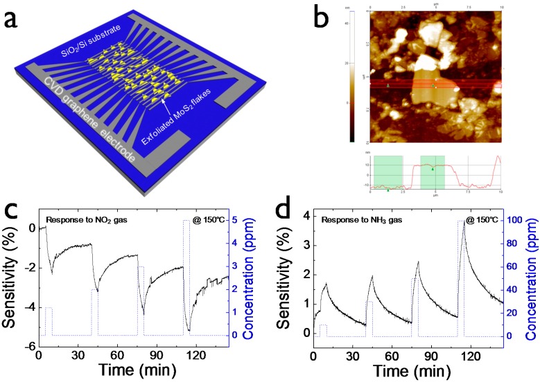
Figure 1a shows a schematic drawing of the gas-sensing device (referred to as graphene/MoS2 device) comprised of mechanically exfoliated MoS2 flakes and CVD-synthesized graphene which function as an active channel for gas molecule detection and electrode for charge collection, respectively. Interdigitated electrode array structure was selected for higher device yield by increasing a probability that MoS2 flakes bridge two graphene electrode lines. The height of the MoS2 flakes connecting two graphene electrode lines was measured to be approximately 20 nm (Figure 1b). Flakes randomly distributed on the substrate have some thickness variation in the range of a few tens of nanometer scale.
Figure 1.
(a) Schematic image of the gas-sensing device consisting of mechanically exfoliated MoS2 flake channels and CVD-synthesized graphene electrodes; (b) AFM morphology of MoS2 flake connecting patterned graphene lines; Bottom indicates a height profile of MoS2. Transient response to (c) NO2 concentration of 1.2 to 5 ppm and (d) NH3 concentration of 10 to 100 ppm, respectively. All gas-sensing tests were carried out at an operating temperature of 150 °C.
We monitored the resistance change of the graphene/MoS2 device when exposed to analyte gas (NO2 or NH3). Sensitivity was defined as ∆R/Ra = (Rg − Ra)/Ra, where Ra and Rg indicates the resistance of the sensor under air and analyte gas, respectively. Figure 1c shows the sensitivity of the graphene/MoS2 sensing device under exposure to NO2 gas concentrations of 1.2, 2, 3, and 5 ppm. All gas-sensing tests were carried out at 150 °C operating temperature since its gas-sensing performance was optimized under this condition. Gas molecules can be strongly adsorbed onto the surface of 2D materials [33]. For desorption of the adsorbed molecules, a thermal or light energy source is necessary, enabling reversible sensing characteristics. Specifically, NO2 gas molecules resulted in negative sensitivity (i.e., resistance decrease). With the increase of NO2 concentration, the absolute sensitivity value also increased. On the contrary, NH3 gas molecules caused positive sensitivity (i.e., resistance increase), as seen in Figure 1d. As the NH3 concentration increased from 10 to 100 ppm, the sensitivity also increased. At the same concentration, the response to NO2 was much more sensitive responded than to NH3. It is responsible for relatively high adsorption energy of NO2 molecules [34,35]. The resistance change of the gas-sensing device is based on charge-transfer phenomena between gas molecules and 2D materials [26]. It is well-known that NO2 and NH3 analyte gas molecules commonly behave as electron acceptors and electron donors, respectively [5]. Interestingly, the graphene/MoS2 gas sensor worked as if it is a p-type device. We propose that the high work function of graphene (4.7 eV) makes it easily hole transport toward the valence band edge of MoS2 [36]. It is unlike the n-type behavior commonly found in low work function metal-MoS2 junction devices where electrons are a major carriers governing the charge transport. Thus, hole carriers involved in charge transfer of graphene/MoS2 device are modulated by gas molecules.
3.2. Metal Decoration Effect on Graphene/MoS2 Gas-Sensing Properties
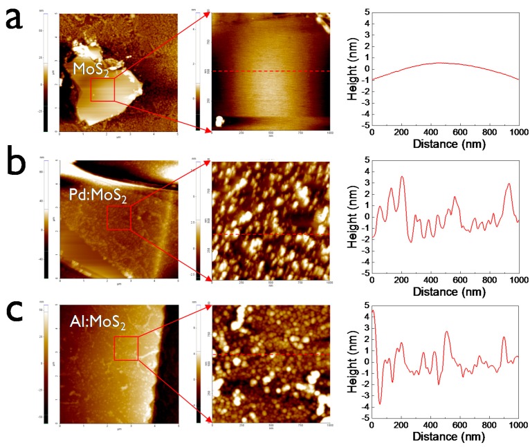
In order to investigate the influence of metal NPs on the gas-sensing properties of MoS2, various metal NPs were deposited on the MoS2. We made three kinds of sensing devices with bare MoS2 and MoS2 decorated with Pd or Al NPs (denoted as MoS2, Pd:MoS2, and Al:MoS2 device, respectively). Before the electrical tests, we examined the surface morphology and height profiles of the metal-decorated MoS2. Basically, the morphology of MoS2 without metal NPs was ultra-smooth and flat (Figure 2a), indicating the layered structure of van der Waals materials.
Figure 2.
AFM morphology images and height profiles of (a) MoS2, (b) Pd:MoS2, and (c) Al:MoS2 on Si/SiO2 substrate.
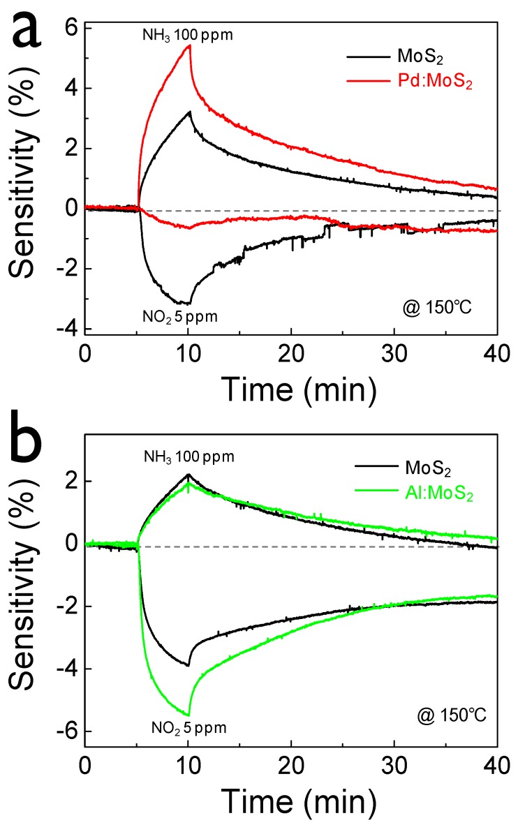
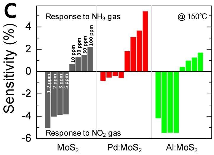
As shown in Figure 2b, Pd NPs were randomly distributed on the MoS2 surface and they aggregated in part. On the other hand, in the case of Al:MoS2, Al formed relatively dense and more fine particles. The morphology properties might strongly depend on physical interaction between MoS2 and metals. The relatively weak interaction between Al metal and MoS2 forms fine NPs. To investigate the effect of metal NPs on the gas-sensing properties, we checked the gas-sensing characteristics before/after the formation of metal NPs. After the deposition of Pd NPs on MoS2, NH3 sensitivity (@ 100 ppm) increased by 70% while NO2 sensitivity (@ 5 ppm) decreased significantly (Figure 3a). However, the opposite trend was observed for the case of Al:MoS2 (Figure 3b). Specifically, the NO2 sensitivity of the Al:MoS2 device was enhanced by around 40%. On the contrary, Al NPs decreased the response to NH3 slightly. Also, we tested the gas response characteristics under different concentrations. From the gas-sensing test results under various gas concentrations (Figure 3c), it was found that Al NPs on MoS2 film is most effective to detect NO2 gas. Pd NPs was more helpful for detecting NH3 gas on MoS2. Consequently, Pd NPs improved NH3 selectivity to NO2 while Al NPs increased the selectivity of NO2 to NH3. In particular, the sensor with a continuous metal network film shows negligible gas responses since the charge transport of the device is dominated by the metal conductive path rather than the MoS2 semiconducting channel.
Figure 3.
Transient gas responses under NH3 100 ppm and NO2 5 ppm before/after (a) Pd decoration on MoS2 and (b) Al decoration on MoS2; (c) Sensitivity summary of MoS2, Pd:MoS2, and Al:MoS2.
The effects of metal decoration on sensing properties have been explained by chemical sensitization or electronic sensitization [37]. A chemical sensitization effect indicates that metal NPs on a sensing film increase the overall active sensing surface area and thereby the adsorption sites of gas molecules. Electronic sensitization can be also considered as a potential mechanism of the sensitivity tuning for each different metal [37]. Thus, it would be potentially agreeable that changes in the sensitivity in our devices are dominated by the latter model rather than the former. For more clarity, the band-bending attributed to the charge transfer between metal (Pd or Al) and semiconductor MoS2 was proposed (Figure S1 of Supplementary Information). Pd metal with high work function increases the hole concentration of the graphene/MoS2 device [38]. Such a p-doping effect of Pd on MoS2 enhances the gas response to NH3 (an electron donor molecule). This is similar to the previous study in which SnO2 nanocrystals act as strong p-type dopants for MoS2 nanosheets [39]. However, low work function Al metal depletes the hole carriers of the device and thereby increases the sensitivity of NO2 (an electron withdrawing molecule). Metal decoration on graphene/MoS2 hybrid structures modifies the electronic properties, which in turn modulates the gas-sensing characteristics. Thus, it would be a useful and simple strategy for achieving a highly selective sensor to a certain analyte gas molecule.
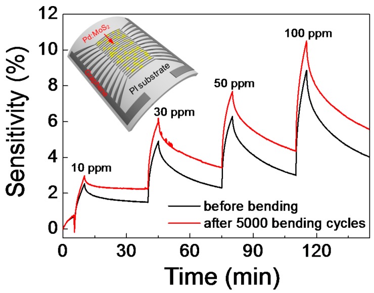
Next, we turned our focus to potential uses of the flexible gas sensor. The whole device region of Pd:MoS2 including graphene electrodes was transferred from a SiO2/Si wafer to a polyimide (PI) substrate (see Experimental Section for the detailed method). The NH3 gas-sensing characteristics of the device were obtained at 150 °C, which is necessary for reversible sensing tests (Figure 4). The glass transition temperature of the PI film is high over 250 °C so that the device can endure the heating conditions. Bent condition with a bending radius of 1.9 mm was applied to the flexibility test. The inset of Figure 4 shows a schematic image of Pd:MoS2 with graphene electrodes on PI substrate. Even if there is an upward shift in sensitivity with increasing gas concentration, the device did not experience any serious change in terms of sensing performance of the Pd:MoS2 flexible device before/after 5000 bending cycles. The cyclic gas-sensing performance was also tested for feasibility, showing a highly reproducible sensing behavior over repetitive sensing cycles (Figure S2 of Supplementary Information). Thus, highly sensitive and reliable gas-sensing performance was achieved in the flexible 2D hybrid structure with metal NPs, indicating a promising route toward the development of wearable electronic sensors.
Figure 4.
NH3 gas response characteristics of flexible Pd:MoS2 gas-sensing device before/after the bending cycle test. The inset shows a 3D schematic image of the bent device.
4. Conclusions
Herein, we demonstrated metal-decorated gas-sensing devices based on a 2D graphene/MoS2 hybrid structure. Metal NPs could modulate the electronic properties of the 2D device, thereby modulating the selectivity towards a certain gas molecule. Specifically, Pd NPs electronically sensitized NH3 gas molecules while Al NPs enhanced NO2 sensitivity. The hybridization process of metal NPs and 2D materials could enable highly sensitive flexible gas sensors along with high bending endurance and stability. Ultimately, the strategy could open an avenue toward wearable sensing platforms.
Acknowledgments
This study was supported by the Fundamental Research Program (PNK4210) of the Korean Institute of Materials Science (KIMS). Also, this work is supported by the Basic Science Research Program of the National Research Foundation of Korea (NRF) funded by the Ministry of Science, ICT & Future Planning (NRF-2014R1A1A1036139 and NRF-2014R1A1A1006214).
Supplementary Files
Author Contributions
B.C. and M.G.H. designed and supervised the experiments; B.C., J.Y., S.K.L., A.R.K., and S.-Y.C. did the experiments; B.C., J.Y., D.-H.K., K.-H.L., B.H.L., and H.C.K. analyzed the data; B.C., J.Y., and M.G.H. wrote the paper.
Conflicts of Interest
The authors declare no conflict of interest.
References
- 1.Schwierz F. Graphene transistors. Nat. Nanotechnol. 2010;5:487–496. doi: 10.1038/nnano.2010.89. [DOI] [PubMed] [Google Scholar]
- 2.Sun Y., Wu Q., Shi G. Graphene based new energy materials. Energy Environ. Sci. 2011;4:1113–1132. doi: 10.1039/c0ee00683a. [DOI] [Google Scholar]
- 3.Gan X., Shiue R.-J., Gao Y., Meric I., Heinz T.F., Shepard K., Hone J., Assefa S., Englund D. Chip-integrated ultrafast graphene photodetector with high responsivity. Nat. Photonics. 2013;7:883–887. doi: 10.1038/nphoton.2013.253. [DOI] [Google Scholar]
- 4.Wu Z.-S., Pei S., Ren W., Tang D., Gao L., Liu B., Li F., Liu C., Cheng H.-M. Field Emission of Single-Layer Graphene Films Prepared by Electrophoretic Deposition. Adv. Mater. 2009;21:1756–1760. doi: 10.1002/adma.200802560. [DOI] [Google Scholar]
- 5.Schedin F., Geim A.K., Morozov S.V., Hill E.W., Blake P., Katsnelson M.I., Novoselov K.S. Detection of individual gas molecules adsorbed on graphene. Nat. Mater. 2007;6:652–655. doi: 10.1038/nmat1967. [DOI] [PubMed] [Google Scholar]
- 6.Kim K.S., Zhao Y., Jang H., Lee S.Y., Kim J.M., Kim K.S., Ahn J.-H., Kim P., Choi J.-Y., Hong B.H. Large-scale pattern growth of graphene films for stretchable transparent electrodes. Nature. 2009;457:706–710. doi: 10.1038/nature07719. [DOI] [PubMed] [Google Scholar]
- 7.Novoselov K.S., Fal’ko V.I., Colombo L., Gellert P.R., Schwab M.G., Kim K. A roadmap for graphene. Nature. 2012;490:192–200. doi: 10.1038/nature11458. [DOI] [PubMed] [Google Scholar]
- 8.Zhang X., Qiao X.-F., Shi W., Wu J.-B., Jiang D.-S., Tan P.-H. Phonon and Raman scattering of two-dimensional transition metal dichalcogenides from monolayer, multilayer to bulk material. Chem. Soc. Rev. 2015;44:2757–2785. doi: 10.1039/C4CS00282B. [DOI] [PubMed] [Google Scholar]
- 9.Wang H., Yuan H., Sae Hong S., Li Y., Cui Y. Physical and chemical tuning of two-dimensional transition metal dichalcogenides. Chem. Soc. Rev. 2015;44:2664–2680. doi: 10.1039/C4CS00287C. [DOI] [PubMed] [Google Scholar]
- 10.Wang Q.H., Kalantar-Zadeh K., Kis A., Coleman J.N., Strano M.S. Electronics and optoelectronics of two-dimensional transition metal dichalcogenides. Nat. Nanotechnol. 2012;7:699–712. doi: 10.1038/nnano.2012.193. [DOI] [PubMed] [Google Scholar]
- 11.Fiori G., Bonaccorso F., Iannaccone G., Palacios T., Neumaier D., Seabaugh A., Banerjee S.K., Colombo L. Electronics based on two-dimensional materials. Nat. Nanotechnol. 2014;9:768–779. doi: 10.1038/nnano.2014.207. [DOI] [PubMed] [Google Scholar]
- 12.Tan C., Liu Z., Huang W., Zhang H. Non-volatile resistive memory devices based on solution-processed ultrathin two-dimensional nanomaterials. Chem. Soc. Rev. 2015;44:2615–2628. doi: 10.1039/C4CS00399C. [DOI] [PubMed] [Google Scholar]
- 13.Tan C., Zhang H. Two-dimensional transition metal dichalcogenide nanosheet-based composites. Chem. Soc. Rev. 2015;44:2713–2731. doi: 10.1039/C4CS00182F. [DOI] [PubMed] [Google Scholar]
- 14.Li H., Wu J., Yin Z., Zhang H. Preparation and Applications of Mechanically Exfoliated Single-Layer and Multilayer MoS2 and WSe2 Nanosheets. Acc. Chem. Res. 2014;47:1067–1075. doi: 10.1021/ar4002312. [DOI] [PubMed] [Google Scholar]
- 15.Huang X., Tan C., Yin Z., Zhang H. 25th Anniversary Article: Hybrid Nanostructures Based on Two-Dimensional Nanomaterials. Adv. Mater. 2014;26:2185–2204. doi: 10.1002/adma.201304964. [DOI] [PubMed] [Google Scholar]
- 16.Huang X., Zeng Z., Zhang H. Metal dichalcogenide nanosheets: preparation, properties and applications. Chem. Soc. Rev. 2013;42:1934–1946. doi: 10.1039/c2cs35387c. [DOI] [PubMed] [Google Scholar]
- 17.Radisavljevic B., Radenovic A., Brivio J., Giacometti V., Kis A. Single-layer MoS2 transistors. Nat. Nanotechnol. 2011;6:147–150. doi: 10.1038/nnano.2010.279. [DOI] [PubMed] [Google Scholar]
- 18.Lee G., Yu Y., Cui X., Petrone N., Lee C., Choi S., Lee D., Lee C., Yoo W.J., Watanabe K., et al. Flexible and Transparent MoS2 Field-Effect Transistors on Hexagonal Boron Nitride-Graphene Heterostructures. ACS Nano. 2013;7:7931–7936. doi: 10.1021/nn402954e. [DOI] [PubMed] [Google Scholar]
- 19.Wang H., Yu L., Lee Y.-H., Shi Y., Hsu A., Chin M.L., Li L.-J., Dubey M., Kong J., Palacios T. Integrated circuits based on bilayer MoS2 transistors. Nano Lett. 2012;12:4674–4680. doi: 10.1021/nl302015v. [DOI] [PubMed] [Google Scholar]
- 20.Lopez-Sanchez O., Lembke D., Kayci M., Radenovic A., Kis A. Ultrasensitive photodetectors based on monolayer MoS2. Nat. Nanotechnol. 2013;8:497–501. doi: 10.1038/nnano.2013.100. [DOI] [PubMed] [Google Scholar]
- 21.Yin Z., Li H., Li H., Jiang L., Shi Y., Sun Y., Lu G., Zhang Q., Chen X., Zhang H. Single-Layer MoS2 Phototransistors. ACS Nano. 2012;6:74–80. doi: 10.1021/nn2024557. [DOI] [PubMed] [Google Scholar]
- 22.Late D.J., Huang Y., Liu B., Acharya J., Shirodkar S.N., Luo J. Sensing Behavior of Atomically Thin-Layered MoS2 Transistors. ACS Nano. 2013;7:4879–4891. doi: 10.1021/nn400026u. [DOI] [PubMed] [Google Scholar]
- 23.Perkins F.K., Friedman A.L., Cobas E., Campbell P.M., Jernigan G.G., Jonker B.T. Chemical vapor sensing with monolayer MoS2. Nano Lett. 2013;13:668–673. doi: 10.1021/nl3043079. [DOI] [PubMed] [Google Scholar]
- 24.Cho B., Yoon J., Lim S.K., Kim A.R., Kim D.-H., Park S.-G., Kwon J.-D., Lee Y.-J., Lee K.-H., Lee B.H., et al. Chemical Sensing of 2D Graphene/MoS2 Heterostructure device. ACS Appl. Mater. Interfaces. 2015;7:16775–16780. doi: 10.1021/acsami.5b04541. [DOI] [PubMed] [Google Scholar]
- 25.Cho B., Kim A.R., Park Y., Yoon J., Lee Y.-J., Lee S., Yoo T.J., Kang C.G., Lee B.H., Ko H.C., et al. Bifunctional Sensing Characteristics of Chemical Vapor Deposition Synthesized Atomic-Layered MoS2. ACS Appl. Mater. Interfaces. 2015;7:2952–2959. doi: 10.1021/am508535x. [DOI] [PubMed] [Google Scholar]
- 26.Cho B., Hahm M.G., Choi M., Yoon J., Kim A.R., Lee Y.-J., Park S.-G., Kwon J.-D., Kim C.S., Song M., et al. Charge-transfer-based Gas Sensing Using Atomic-layer MoS2. Sci. Rep. 2015;5 doi: 10.1038/srep08052. [DOI] [PMC free article] [PubMed] [Google Scholar]
- 27.Geim A.K., Grigorieva I.V. Van der Waals heterostructures. Nature. 2013;499:419–425. doi: 10.1038/nature12385. [DOI] [PubMed] [Google Scholar]
- 28.Lee C.-H., Lee G.-H., van der Zande A.M., Chen W., Li Y., Han M., Cui X., Arefe G., Nuckolls C., Heinz T.F., et al. Atomically thin p–n junctions with van der Waals heterointerfaces. Nat. Nanotechnol. 2014;9:676–681. doi: 10.1038/nnano.2014.150. [DOI] [PubMed] [Google Scholar]
- 29.Hong X., Kim J., Shi S.-F., Zhang Y., Jin C., Sun Y., Tongay S., Wu J., Zhang Y., Wang F. Ultrafast charge transfer in atomically thin MoS2/WS2 heterostructures. Nat. Nanotechnol. 2014;9:682–686. doi: 10.1038/nnano.2014.167. [DOI] [PubMed] [Google Scholar]
- 30.Yu L., Lee Y.H., Ling X., Santos E.J.G., Shin Y.C., Lin Y., Dubey M., Kaxiras E., Kong J., Wang H., et al. Graphene/MoS2 Hybrid technology for large-scale two-dimensional electronics. Nano Lett. 2014;14:3055–3063. doi: 10.1021/nl404795z. [DOI] [PubMed] [Google Scholar]
- 31.Zhang W., Chuu C.-P., Huang J.-K., Chen C.-H., Tsai M.-L., Chang Y.-H., Liang C.-T., Chen Y.-Z., Chueh Y.-L., He J.-H., et al. Ultrahigh-gain photodetectors based on atomically thin graphene-MoS2 heterostructures. Sci. Rep. 2014;4 doi: 10.1038/srep03826. [DOI] [PMC free article] [PubMed] [Google Scholar]
- 32.Geim A.K. Graphene: Status and Prospects. 2009;324:1530–1535. doi: 10.1126/science.1158877. [DOI] [PubMed] [Google Scholar]
- 33.Randeniya L.K., Shi H., Barnard A.S., Fang J., Martin P.J., Ostrikov K.K. Harnessing the Influence of Reactive Edges and Defects of Graphene Substrates for Achieving Complete Cycle of Room-Temperature Molecular Sensing. Small. 2013;9:3993–3999. doi: 10.1002/smll.201300689. [DOI] [PubMed] [Google Scholar]
- 34.Zhang Y.-H., Chen Y.-B., Zhou K.-G., Liu C.-H., Zeng J., Zhang H.-L., Peng Y. Improving gas sensing properties of graphene by introducing dopants and defects: A first-principles study. Nanotechnology. 2009;20 doi: 10.1088/0957-4484/20/18/185504. [DOI] [PubMed] [Google Scholar]
- 35.Zhou M., Lu Y.-H., Cai Y.-Q., Zhang C., Feng Y.-P. Adsorption of gas molecules on transition metal embedded graphene: A search for high-performance graphene-based catalysts and gas sensors. Nanotechnology. 2011;22 doi: 10.1088/0957-4484/22/38/385502. [DOI] [PubMed] [Google Scholar]
- 36.Kwak J.Y., Hwang J., Calderon B., Alsalman H., Munoz N., Schutter B., Spencer M.G. Electrical Characteristics of Multilayer MoS2 FET’s with MoS2/Graphene Heterojunction Contacts. Nano Lett. 2014;14:4511–4516. doi: 10.1021/nl5015316. [DOI] [PubMed] [Google Scholar]
- 37.Franke M.E., Koplin T.J., Simon U. Metal and metal oxide nanoparticles in chemiresistors: Does the nanoscale matter? Small. 2006;2:36–50. doi: 10.1002/smll.200500261. [DOI] [PubMed] [Google Scholar]
- 38.Kim B.-K., Park N., Na P.S., So H.-M., Kim J.-J., Kim H., Kong K.-J., Chang H., Ryu B.-H., Choi Y., et al. The effect of metal cluster coatings on carbon nanotubes. Nanotechnology. 2006;17:496–500. [Google Scholar]
- 39.Cui S., Wen Z., Huang X., Chang J., Chen J. Stabilizing MoS2 Nanosheets through SnO2 Nanocrystal Decoration for High-Performance Gas Sensing in Air. Small. 2015;11:2305–2313. doi: 10.1002/smll.201402923. [DOI] [PubMed] [Google Scholar]
Associated Data
This section collects any data citations, data availability statements, or supplementary materials included in this article.


