Abstract
The structural, electronic, transport and optical properties of black phosphorus/MoS2 (BP/MoS2) van der Waals (vdw) heterostructure are investigated by using first principles calculations. The band gap of BP/MoS2 bilayer decreases with the applied normal compressive strain and a semiconductor-to-metal transition is observed when the applied strain is more than 0.85 Å. BP/MoS2 bilayer also exhibits modulation of its carrier effective mass and carrier concentration by the applied compressive strain, suggesting that mobility engineering and good piezoelectric effect can be realized in BP/MoS2 heterostructure. Because the type-II band alignment can facilitate the separation of photo-excited electrons and holes, and it can benefit from the great absorption coefficient in ultra-violet region, the BP/MoS2 shows great potential to be a very efficient ultra-violet photodetector.
Despite being a very promising two-dimensional (2D) material, gapless graphene has limitation in its applications in nanoelectronics and optoelectronics1,2,3. As alternatives, new researches have emerged focusing on other 2D materials such as transition metal sulfides (TMDs), which possess sizable band gap and display advantageous optoelectronic properties4,5,6,7. For example, bulk MoX2 (X = S, Se, Te) and WX2 are indirect band gap semiconductors, whereas their monolayers have direct band gaps, which are favorable for optoelectronic applications. The single-layer MoS2 based field-effect transistors exhibit an excellent current on/off ratio of 108 8, and the application of monolayer MoS2 in integrated circuits and logic operations has already been realized9.
Recently, a new 2D layered material, namely black phosphorus (BP) has been fabricated by several research groups10,11,12. Similar to other 2D materials, different BP layers binding together via the weak van der Waals (vdW) force. Theoretical calculations show that the band gap of BP is layer dependent with 0.30 eV in bulk BP and 0.90 eV in its monolayer form12,13,14,15. What’s more, bulk BP shows a high hole mobility up to 10000 cm2/Vs16. And well-behaved p-type field-effect transistors with mobilities of up to 1000 cm2/Vs have been demonstrated on few-layer BP10. These properties make BP a potential candidate for novel applications in nanoelectronics and optoelectronics.
Recent studies have shown that hybrid systems consisting of various 2D materials would provide more opportunities for achieving desired electronic and optoelectronic properties17,18,19,20,21. For example, remarkable multiple optoelectronic functionality, including highly sensitive photodetection and gate-tunable persistent photoconductivity has been observed in the graphene/MoS2 vdW heterostructures22. The vertical field-effect transistors based on the graphene-WS2 heterostructures are also fabricated with unprecedented current modulation exceeding 106 at room temperature23. Moreover, Yexin Deng etc demonstrated that a gate-tunable p-n diode based on a p-type BP/n-type monolayer MoS2 vdw p-n heterojunction shows a maximum photodetection responsivity of 418 mA/W at the wavelength of 633 nm24. An anomalous photoluminescence quenching is observed in artificial heterostacks of monolayer TMDs and few-layer BP25. J. E. Padilha etc reported that the Schottky barrier height and doping of phosphorus can be controlled by applying an external perpendicular electric field26.
In this work, we investigate the effect of normal compressive strain on the structural, electronic, transport and optical properties of semiconducting BP/MoS2 vdW heterostructure. The band gap of BP/MoS2 decreases with the applied strain and a semiconductor-to-metal transition is observed when the applied compressive strain is more than 0.85 Å. The compressive strain also exerts influence on the charge carrier effective mass and concentration, suggesting that mobility engineering and good piezoelectric effect can be realized in BP/MoS2 heterostructure. The calculated optical property of BP/MoS2 shows that BP/MoS2 may be a very efficient ultra-violet photodetector because the type-II band alignment can facilitate the separation of photo-excited electrons and holes, and it can benefit from the great absorption coefficient in ultra-violet region.
Results and Discussion
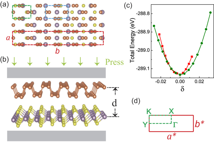
Top and side views of the relaxed atomic structure of BP/MoS2 bilayer are shown in Fig. 1. To minimize the lattice mismatch between the stacking sheets, a rectangular unit cell of MoS2 is constructed. The supercell of this system is composed by 1 × 4 unit cells of BP and 1 × 5 unit cells of MoS2, which is the same with our previous work27. The optimised lattice constants of monolayer MoS2 are aM = 3.19 Å, bM = 5.53 Å and the calculated lattice constants of monolayer BP are aP = 3.30 Å, bP = 4.62 Å. To determine the stable structure of BP/MoS2 bilayer, the total energy as a function of uniaxial strains along X (zigzag) and Y (armchair) directions is depicted in Fig. 1(c). Both curves show their minimas under zero strain, at which point, the lattice constants of the supercell employed here are a = 3.26 Å, b = 22.18 Å.
Figure 1.
(a) Top view and (b) side view of BP/MoS2 bilayer. The green and blue rectangular regions present the unit cells of BP and MoS2. The supercell of BP/MoS2 bilayer is depicted in red rectangular region. (c) Evolution of the total energy of BP/MoS2 bilayer as a function of uniaxial strains. (d) Brillouin zone with high-symmetry points labeled.
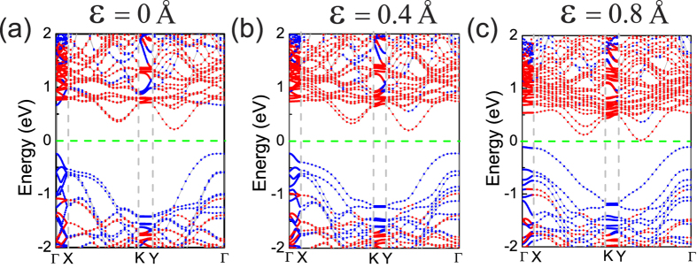
Tuning the band gaps of 2D materials has been a challenge in band gap engineering. Many techniques, such as in-plane strains28,29,30,31 and a strong external electric field32,33, are promising but suffer from lack of practical applicability. Therefore, in this work, the effect of applied normal compressive strain on the electronic and optical properties of BP/MoS2 is studied. The strain is calculated as ε = d0 − d, where d0 and d are the equilibrium and instantaneous distances between the top phosphorus atom layer and the molybdenum atom layer. In Fig. 2, we show the projected band structure of BP/MoS2 bilayer under different compressive strain. Figure 1(d) presents the Brillouin zone of rectangular cells with high-symmetry points labeled. In Fig. 2, the bands dominated by BP and MoS2 are plotted by blue red dots, respectively. It is clear that the conduction band minimum (CBM) and the valence band maximum (VBM) are dominated by MoS2 and BP, respectively, regardless of the applied compressive strain. More importantly, BP/MoS2 vdW heterostructure has a type-II band alignment and thus the lowest energy electron-hole pairs are spatially separated with electrons and holes locating in MoS2 and BP layer, respectively. These results indicate that BP/MoS2 vdW heterostructure may be suitable for optoelectronics and solar energy conversion.
Figure 2. Evolution of projected band structure of BP/MoS2 bilayer as a function of the applied compressive strain.
The bands dominated by BP and MoS2 are plotted by blue red dots, respectively.
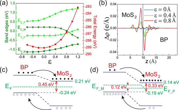
Evolution of band edges and total energy of BP/MoS2 bilayer as a function of the applied compressive strain is concluded in Fig. 3(a). It can be proved that the interlayer distance d0 at equilibrium state is 6.92 Å. The vdW interaction exerts little influence on the band edges of BP/MoS2. The BP/MoS2 bilayer shows a finite indirect band gap up to 0.45 eV. Upon applying compressive strain, both the VBM and CBM move towards the Fermi level, resulting in a decreasing band gap with the applied strain. The BP/MoS2 bilayer experiences a semiconductor-to-metal transition when the applied compressive strain is larger than 0.85 Å, which may lead to tunable conductivity and transport properties.
Figure 3.
(a) Evolution of band edges and total energy of BP/MoS2 bilayer as a function of the applied compressive strain. (b) The difference between the integrated charge density of BP/MoS2 bilayer under different compressive strain and that of the isolated monolayers. (c,d) The band alignment of BP/MoS2 bilayer under applied compressive strain of 0 Å and 0.4 Å, respectively. EF_P(M) is the quasi-fermi level of BP (MoS2) in BP/MoS2 bilayer.
The difference between the integrated charge density of BP/MoS2 bilayer under different compressive strain and that of the isolated monolayers as a function of the perpendicular distance is shown in Fig. 3(b). It is calculated as
 |
where ρs(x, y, z), ρBP(x, y, z) and  are the charge density at the (x, y, z) point in BP/MoS2 supercell, BP and MoS2 monolayer supercell, respectively. It is found that there is a small amount of charge exchange between BP layer to MoS2 layer. Furthermore, the applied compressive strain can facilitate electrons transferring from BP to MoS2 layer and holes transferring from MoS2 to BP layer. More charge transfer between BP layer and MoS2 layer suggests an increased carrier concentration and a stronger interlayer interaction. When under compressive strain, the quasi-fermi level of MoS2 moves upward and the quasi-fermi level of BP layer moves downward, as shown in Fig. 3(c,d). As a result, the band gap of BP/MoS2 bilayer decreases with the applied compressive strain.
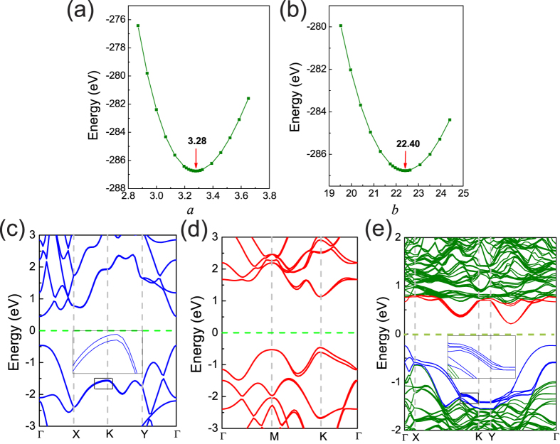
For a three-dimensional material, when it is compressed along z direction, it usually will expand in the planar x and y directions. This effect is also taken into consideration in this work. Figure 4(a,b) gives the variation of the total energy with planar lattice constant, a and b, in BP/MoS2 bilayer under a normal compressive stran of 0.8 Å. It is found that the total energy reaches its minima when a = 3.28 Å, b = 22.40 Å, respectively. Both a and b are a little larger than that of BP/MoS2 bilayer without strains. It can be concluded that for the BP/MoS2 heterostructure, when exerting compressive strain along z direction, it also will expand in the planar x and y direction, just as a three-dimensional material.
Figure 4.
(a,b)The variation of the total energy with planar lattice constant, a and b, in BP/MoS2 bilayer under a normal compressive stran of 0.8 Å. The band structures of BP monolayer, MoS2 monolayer and BP/MoS2 heterostructure, including SOC effect are shown in (c–e) respectively.
Monolayer MoS2 has been reported to have a intrinsic spin-orbit gap. Whether the spin-orbit coupling (SOC) effect will exert obvious influence on the band gap of BP/MoS2 heterostructure is unknown. In Fig. 4(c,d), the band structures of BP and MoS2 monolayer, including SOC effect, are shown. BP and MoS2 monolayer show a spin-orbit gap of 22 meV and 147 meV at K point in the valence band, which are in good agreement with previous works15,34. As shown in Fig. 4(e), though the SOC gap of MoS2 can be comparable to the band gap of the BP/MoS2 heterostructure under compressive strain, the SOC exerts little influence on the band gap of BP/MoS2 because the VBM in the band structure of BP/MoS2 bilayer is dominated by BP whose SOC gap is very small rather than by MoS2. So the SOC effect is not taken into consideration in following results.
With the applied normal compressive strain exerting influence on the band structure of BP/MoS2 bilayer, a change in the effective masses of electrons and holes can be expected. Figure 5 displays the changes of electron and hole effective masses with the compressive strain. The effective mass is calculated using  , and the k points closely approach the VBM and CBM. In the band structure of BP/MoS2 bilayer, it is clear that the CBM is located at a point between Y and Γ. The curve labeled CBM[Y] shows the effective mass of electron at CBM along Y direction. The electron effective mass (me) at CBM in the Γ direction is much smaller than that in the Y direction and it decreases gradually with applied compressive strain. The hole effective mass (mh) at Γ is quite sensitive to the compressive strain. mh in the X direction increases drastically in the case of compressive strain larger than 0.4 Å, while that in the Y direction decreases gradually with the compressive strain. It also can be seen that the minimum of both me and mh is much smaller than 1, suggesting that BP/MoS2 as a type-II heterostructure may possesses great transport properties such as high mobility and conductivity. BP/MoS2 vdW heterostructure may have great potential for applications in nanoelectronics and optoelectronics.
Figure 5.
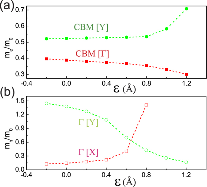
Effective masses (in units of electron mass m0) of (a) electrons and (b) holes as a function of applied compressive strain. The masses are labeled by the band extremum and the direction (in square brackets) along which the mass is calculated. The vertical dashed line indicates unstrained BP/MoS2.
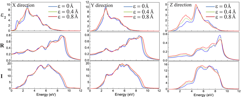
Very recently, it is predicted that the BP/TMD system is a more efficient solar cell than the graphene/TMD systems35,36,37 because the former can benefit from the absorption of wider range of wavelength in the solar spectrum, and the type-II heterojunction alignment can allow more efficient hole-electron separation. In Fig. 6, therefore, the real (ε1) and imaginary (ε2) parts of the frequency-dependent dielectric functions are calculated by GGA-PBE and the frequency-dependent reflectivity R and absorption coefficient I are computed. Different with hexagonal lattice, the dielectric tensor has three independent components, namely, εX, εY and ε⊥. Strong anisotropy is observed in the imaginary parts of dielectric functions  ,
,  and
and  . The variations of reflectivity and absorption coefficients as the function of frequency also exhibit similar trend, as illustrated in middle and bottom planets. From the absorption spectrum (the bottom planet), we can find that BP/MoS2 bilayer may have good application in ultraviolet light (above 3.27 eV) detecting. Furthermore, the effect of applied normal compressive strain on the optical properties of BP/MoS2 bilayer is also studied. The applied compressive strain shows little influence on the optical properties in the X and Y directions, while exerts much more remarkable influence on the three optical parameters in perpendicular direction (
 , R⊥ and I⊥). It is because the compressive strain just enhances the interlayer interaction while exerts no influence on the in-plane interaction.
Figure 6.
Calculated optical properties in (a) X directin, (b) Y direction and (c) perpendicular direction of BP/MoS2 bilayer under different compressive strain. From top to bottom planets are imaginary part of the dielectric function ε2, reflectivity R and absorption coefficient I, respectively.
Conclusion
In summary, we have provided total energy and band structure calculations for the p-type BP/n-type MoS2 vdW heterostructure and investigated its structural, electronic, transport and optical properties by using first principles calculations. The decreased band gap by applied compressive strain indicates the great application potential of BP/MoS2 vdW heterostructures in future nanoelectronics such as field effect transistors. A semiconductor-to-metal transition can be observed in BP/MoS2 bilayer under the compressive strain. The reduced carrier effective mass and improved carrier concentration by the applied compressive strain suggest that mobility engineering and good piezoelectric effect can be realized in BP/MoS2 bilayer. Furthermore, because the type-II heterojunction alignment can facilitate the separation of photo-excited electrons and holes, and it can benefit from the great absorption coefficient in ultra-violet region the BP/MoS2 heterostructure may be a very efficient ultra-violet photodetector. According to our results, the BP/MoS2 vdw p-n heterojuntion will present abundant opportunities for application in future nano- and optoelectronics such as photovoltaic cell, photodetector and logical device.
Methods
The first-principles calculations are performed by VASP code within plane-wave basis sets and Perdew-Burke-Ernzerhof (PBE) projector augmented wave pseudopotentials38,39,40. The semi-empirical DFT-D2 method method of Grimme is utilized for the dispersion correction in the interlayer interaction41. The plane-wave cutoff energy is set to be 500 eV and a vacuum larger than 12 Å is used to simulate the isolated sheet. The first Brillouin zone is sampled with a (15 × 15 × 1) Monkhorst-Pack grid for relaxation of BP and MoS2 unitcells42. A (5 × 20 × 1) Monkhorst-Pack grid is used for relaxation of supercells. All the structures are fully relaxed with a force tolerance of 0.01 eV/Å.
Additional Information
How to cite this article: Huang, L. et al.Strain induced piezoelectric effect in black phosphorus and MoS2 van der Waals heterostructure. Sci. Rep.5, 16448; doi: 10.1038/srep16448 (2015).
Acknowledgments
This work was supported by the National Natural Science Foundation of China under Grant No. 91233120 and the National Basic Research Program of China (2011CB921901). Jingbo Li thankfully acknowledge financial support from the CAS/SAFEA International Partnership Program for Creative Research Teams. Zhongming Wei acknowledges financial support from the “Hundred Talents Program” of Chinese Academy of Sciences.
Footnotes
Author Contributions Every author has made contribution to the manuscript. L.H. performed the density functional theory calculations. L.H. and Y.L. wrote the manuscript. Z.W. and J.L. guide the work.
References
- Geim A. K. Graphene: status and prospects. Science 324, 1530–1534 (2009). [DOI] [PubMed] [Google Scholar]
- Avouris P., Chen Z. & Perebeinos V. Carbon-based electronics. Nat. Nanotechnol. 2, 605–615 (2007). [DOI] [PubMed] [Google Scholar]
- Schwierz F. Graphene transistors. Nat. Nanotechnol. 5, 487–496 (2010). [DOI] [PubMed] [Google Scholar]
- Tsai D.-S. et al.Few-layer MoS2 with high broadband photogain and fast optical switching for use in harsh environments. ACS Nano 7, 3905–3911 (2013). [DOI] [PubMed] [Google Scholar]
- Lopez-Sanchez O. et al.Ultrasensitive photodetectors based on monolayer MoS2. Nat. Nanotechnol. 8, 497–501 (2013). [DOI] [PubMed] [Google Scholar]
- Coleman J. N. et al.Two-dimensional nanosheets produced by liquid exfoliation of layered materials. Science 331, 568–571 (2011). [DOI] [PubMed] [Google Scholar]
- Korn T. et al.Low-temperature photocarrier dynamics in monolayer MoS2. Appl. Phys. Lett. 99, 102109 (2011). [Google Scholar]
- Radisavljevic B. et al.Single-layer MoS2 transistors. Nat. Nanotechnol. 6, 147–150 (2011). [DOI] [PubMed] [Google Scholar]
- Radisavljevic B., Whitwick M. B. & Kis A. Integrated circuits and logic operations based on single-layer MoS2. ACS Nano 5, 9934–9938 (2011). [DOI] [PubMed] [Google Scholar]
- Li L. et al.Black phosphorus field-effect transistors. Nat. Nanotechnol. 9, 372–377 (2014). [DOI] [PubMed] [Google Scholar]
- Castellanos-Gomez A. et al.Isolation and characterization of few-layer black phosphorus. 2D Mater. 1, 025001 (2014). [Google Scholar]
- Liu H. et al.Phosphorene: an unexplored 2D semiconductor with a high hole mobility. ACS Nano 8, 4033–4041 (2014). [DOI] [PubMed] [Google Scholar]
- Yan Li S. Y. & Li J. Modulation of the electronic properties of ultrathin black phosphorus by strain and electrical field. J. Phys. Chem. C 118, 23970–23976 (2014). [Google Scholar]
- Tran V., Soklaski R., Liang Y. & Yang L. Layer-controlled band gap and anisotropic excitons in few-layer black phosphorus. Phys. Rev. B 89, 235319 (2014). [Google Scholar]
- Rudenko A. N. & Katsnelson M. I. Quasiparticle band structure and tight-binding model for single-and bilayer black phosphorus. Phys. Rev. B 89, 201408 (2014). [Google Scholar]
- Morita A. Semiconducting black phosphorus. Appl. Phys. A:Solids Surf. 39, 227–242 (1986). [Google Scholar]
- Peng X. & Ahuja R. Symmetry breaking induced bandgap in epitaxial graphene layers on SiC. Nano Lett. 8, 4464–4468 (2008). [DOI] [PubMed] [Google Scholar]
- Britnell L. et al.Field-effect tunneling transistor based on vertical graphene heterostructures. Science 335, 947–950 (2012). [DOI] [PubMed] [Google Scholar]
- Behera H. & Mukhopadhyay G. Strain-tunable band gap in graphene/h-BN hetero-bilayer. J. Phys. Chemi. Solids 73, 818–821 (2012). [Google Scholar]
- Bertolazzi S., Krasnozhon D. & Kis A. Nonvolatile memory cells based on MoS2/graphene heterostructures. ACS Nano 7, 3246–3252 (2013). [DOI] [PubMed] [Google Scholar]
- Balu R., Zhong X., Pandey R. & Karna S. P. Effect of electric field on the band structure of graphene/boron nitride and boron nitride/boron nitride bilayers. Appl. Phys. Lett. 100, 052104 (2012). [Google Scholar]
- Roy K. et al.Graphene-MoS2 hybrid structures for multifunctional photoresponsive memory devices. Nature Nanotechnol. 8, 826–830 (2013). [DOI] [PubMed] [Google Scholar]
- Georgiou T. et al.Vertical field-effect transistor based on graphene-WS2 heterostructures for flexible and transparent electronics. Nature Nanotechnol. 8, 100–103 (2013). [DOI] [PubMed] [Google Scholar]
- Deng Y. et al.Black phosphorus–monolayer MoS2 van der waals heterojunction p–n diode. ACS Nano 8, 8292–8299 (2014). [DOI] [PubMed] [Google Scholar]
- Yuan J. et al.Photoluminescence quenching and charge transfer in artificial hetero-stacks of monolayer transition metal dichalcogenides and few-layer black phosphorus. ACS Nano 9, 555–563 (2015). [DOI] [PubMed] [Google Scholar]
- Padilha J., Fazzio A. & da Silva A. J. Van der waals heterostructure of phosphorene and graphene: Tuning the schottky barrier and doping by electrostatic gating. Phys. Rev. Lett. 114, 066803 (2015). [DOI] [PubMed] [Google Scholar]
- Le H. et al.Electric-field tunable band offsets in black phosphorus and MoS2 van der Waals p-n heterostructure. J. Phys. Chem. Lett. 6, 2483–2488 (2015). [DOI] [PubMed] [Google Scholar]
- Scalise E. et al.Strain-induced semiconductor to metal transition in the two-dimensional honeycomb structure of MoS2. Nano Res. 5, 43–48 (2012). [Google Scholar]
- Han X. et al.Strain and orientation modulated bandgaps and effective masses of phosphorene nanoribbons. Nano Lett. 14, 4607–4614 (2014). [DOI] [PubMed] [Google Scholar]
- Fei R. & Yang L. Strain-engineering the anisotropic electrical conductance of few-layer black phosphorus. Nano Lett. 14, 2884–2889 (2014). [DOI] [PubMed] [Google Scholar]
- Peng X., Wei Q. & Copple A. Strain-engineered direct-indirect band gap transition and its mechanism in two-dimensional phosphorene. Phys. Rev. B 90, 085402 (2014). [Google Scholar]
- Ramasubramaniam A., Naveh D. & Towe E. Tunable band gaps in bilayer transition-metal dichalcogenides. Phys. Rev. B 84, 205325 (2011). [Google Scholar]
- Das S. et al.Tunable transport gap in phosphorene. Nano Lett. 14, 5733–5739 (2014). [DOI] [PubMed] [Google Scholar]
- Cheiwchanchamnangi T. & Lambrecht W. Quasiparticle band structure calculation of monolayer, bilayer, and bulk MoS2. Phys. Rev. B 85, 205302 (2012). [Google Scholar]
- Bernardi M., Palummo M. & Grossman J. C. Extraordinary sunlight absorption and one nanometer thick photovoltaics using two-dimensional monolayer materials. Nano Lett. 13, 3664–3670 (2013). [DOI] [PubMed] [Google Scholar]
- Britnell L. et al.Strong light-matter interactions in heterostructures of atomically thin films. Science 340, 1311–1314 (2013). [DOI] [PubMed] [Google Scholar]
- Guo H. et al.Phosphorene nanoribbons, phosphorus nanotubes, and van der waals multilayers. J. Phys. Chem. C 118, 14051–14059 (2014). [Google Scholar]
- Blöchl P. E. Projector augmented-wave method. Phys. Rev. B 50, 17953 (1994). [DOI] [PubMed] [Google Scholar]
- Kresse G. & Furthmuller J. Efficient iterative schemes for ab initio total-energy calculations using a plane-wave basis set. Phys. Rev. B 54, 11169 (1996). [DOI] [PubMed] [Google Scholar]
- Perdew P., Burke K. & Ernzerhof M. Generalized gradient approximation made simple. Phys. Rev. Lett. 77, 3865 (1996). [DOI] [PubMed] [Google Scholar]
- Grimme S. Semiempirical gga-type density functional constructed with a long-range dispersion correction. J. Comput. Chem. 27, 1787–1799 (2006). [DOI] [PubMed] [Google Scholar]
- Monkhorst H. J. & Pack J. D. Special points for brillouin-zone integrations. Phys. Rev. B 13, 5188–5192 (1976). [Google Scholar]


