

Abstract
RNA nanotechnology offer advantages to construct thermally and chemically stable nanoparticles with well-defined shape and structure. Here we report the development of an RNA-Qd (quantum dot) chimera for resistive biomolecular memory application. Each Qd holds two copies of the pRNA three-way junction (pRNA-3WJ) of bacteriophage phi29 DNA-packaging motor. The fixed quantity of two RNA per Qd was achieved by immobilizing pRNA-3WJ harboring Sephadex aptamer for resin binding. Two thiolated pRNA-3WJ serves as two feet of the chimera to stand on the gold plate. The RNA nanostructure served as both an insulator and a mediator to provide defined distance between Qd and gold. Immobilization of chimera nanoparticle was confirmed through scanning tunneling microscopy (STM). As revealed by scanning tunneling spectroscopy (STS), the conjugated pRNA-3WJ-Qd chimera exhibited excellent electrical bi-stability signal for biomolecular memory function, demonstrating great potential for the development of resistive biomolecular memory and nanobio-inspired electronic device for information processing and computing.
Keywords: RNA Nanotechnology, pRNA-quantum dot chimera, Biomolecular electronics, Nanoscale resistive biomolecular memory, Phi29 DNA packaging motor
In 1965, Gordon Moore anticipated that the number of transistors and memory devices per unit area on integrated circuit would double every year due to the information expansion.1 Subsequently, advances in memory devices, transistors and information processors have moved to micro-sized dimension.1,2 The random access memory (RAM) devices are essential for micro-sized computing machines. RAMs are fast, but they are volatile and energy consuming. Si-Flash memory devices represent prominent nonvolatile data memory3 due to high density and low production costs, but suffer from low endurance and low write speed, and require high voltages for write operations. Thus, the semiconductor industry faces many challenges such as integration limitation, heat induction, and energy efficiency. To overcome current limitations, some pioneers of the field proposed molecular electronics.4,5 which showed potential for molecular-level size control and fabrication. Molecular memory devices such as virus-based particles,6 protein-based or inorganic molecule-based devices7-10 have shown promise. However, the addressability of the systems to fabricate molecular memory devices with controllable block assembly utilizing bottom up approach is still limited. Thus, well-defined and easy to assemble nanostructures are needed. Bottom up assembly using proteins or other macromolecules is more challenging due to the complexity in structure, folding, and molecular interaction during assembly. Development of nanoscale resistive biomemory11 based on RNA nanotechnology12 could be an advantageous alternative, especially due to the recently reported addressable bottom up self-assembly property of the three-way junction of bacteriophage phi29 motor pRNA.13
The concept of RNA nanotechnology was first proven in 199814 using the packaging RNA (pRNA)15 derived from bacteriophage phi29 DNA packaging motor. RNA dimers, trimers, and hexamers were assembled from re-engineered RNA fragments via bottom up assembly,16,17 one of the two nanotechnology approaches beside the top-down approach. The pRNA molecule contains two domains, a helical DNA translocation domain and an intermolecular interaction domain.12,13,18 These two domains are connected by a three-way junction (3WJ) motif, which has been found recently to be thermodynamically stable nanostructure motif.13,19-21 The 3WJ remains intact even being diluted to picomolar concentration and remains stable at boiling temperature22 in presence of strong denaturing reagent.13 The thermodynamically stable properties make the pRNA-3WJ motif an ideal building block for constructing various RNA nanoparticles for diverse applications in nanomedicine and nanotechnology.23 A large number of other highly ordered RNA structures have been reported and shown to perform diverse biological functions.24-32
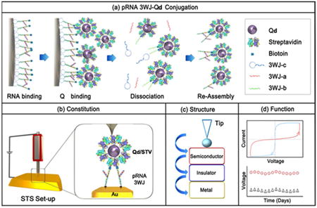
Here we report the use of exceptionally stable pRNA-3WJ to design and construct a new bio-inorganic chimera material that displayed a bi-stable resistive switching biomolecular memory property. The pRNA-3WJ was specifically conjugated to the streptavidin coated quantum dot (Qd/STV). The Qd/STV/Bio-3WJ-SH (Biotin-3WJ-Thio) complex contained one Qd as the head and two thiol-modified 3WJ as feet (Figure 1a) to stand on the gold plate via covalent binding of the SH-group(Figure 1b).33,34 The pRNA-3WJ served as insulator to prevent the Qd from direct contact with the gold (Au) substrate (Figure 1c). This unique structure of RNA-Qd conjugate shows a resistive-switching property, as confirmed by scanning tunneling microscopy (STM) and scanning tunneling spectroscopy (STS) in air condition (Figure 1d).12,35,36
Figure 1. Schematic diagram for experiential design.
(a) Site-specific conjugation method for Qd/STVQd/STV/Bio-3WJ chimera nanoparticle, (b) constitution, (c) expected structure, (d) function. Schematic diagram for experiential design. (a) Site-specific conjugation method for Qd/STVQd/STV/Bio-3WJ chimera nanoparticle, (b) constitution, (c) expected structure, (d) function. 177×123mm (300 × 300 DPI)
Results and Discussion
Experimental Design
In this study, the Qd was used as a semiconducting material to charge and release the electrons. Au was used as a substrate to measure the electric signal. The resistive-switching memory utilized the Qd, pRNA-3WJ, and Au to study the memory function. Qd and Au substrates were separated by pRNA-3WJ, which served both as a connector to bridge, and as a partition to prevent the contact between Qd and Au substrates while keeping them at an appropriate distance. The pRNA-3WJ served as an insulator between the Qd and Au block (Figure 1c). The pRNA-3WJ and Qd was conjugated with a specific binding ratio, with two RNA attached to one Qd, thus serve as feet standing on the Au block. The STM experiment was conducted to detect the pRNA-3WJ/Qd conjugate on the surface, and the tip was positioned onto the pRNA-3WJ/Qd conjugate. The electric potential was applied to the pRNA-3WJ/Qd conjugate utilizing the STS set-up, thereby monitoring the resistive-switching memory function.
Construction of RNA-Qd chimera containing Qd as the head and pRNA-3WJ motif as foot to stand on the gold substrate
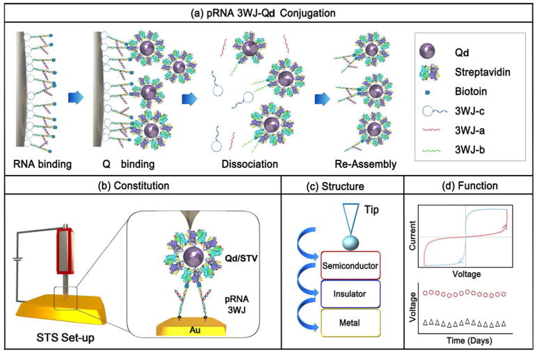
Five steps were carried out to conjugate Qd with pRNA-3WJ. 1) Assemble the 3WJ nanoparticles that contain two functional modules: a biotin and a Sephadex-binding RNA aptamer (SEPapt) (Figure 2a-b); 2) immobilize this SEPapt/Bio-3WJ RNA nanoparticle onto Sephadex resin; 3) incorporate the Qd/STV to the Biotin-3WJ imobiliezed on Sephadex resin; 4) dissociate, by urea/EDTA, and to purify the Qd/STV/Bio-3WJ-b (Figure 2c); 5) re-assemble the Qd/STV/Bio-3WJ-SH chimera (Figure 2e).
Figure 2. Assay for the assembly of pRNA-3WJ/Qd chimera.
(a) 2D structure of the biotinylated pRNA-3WJ containing an aptamer that can bind Sephadex G100. (b) Native PAGE gel with ethidium bromide staining showing the assembly of the RNA structure in (a), Lane 1 is DNA ladder. (c) Native agarose (2% TBE) gel image with ethidium bromide (EB) staining (left panel) and Cy5 fluorescence emission (right panel) showing the purified Qd/STV/Bio-3WJ-b. Lane 1 is 100 base pair DNA ladder. (d) Native agarose gel imaged with ethidium bromide staining (left panel) and Cy5 fluorescence emission (right panel) to titrate the copy number of Bio-3WJ-b binding to each Qd/STV complex using Sephadex G100 immobilization method. (e) Native agarose gel with ethidium bromide staining shows the reassembled Qd/STV/Bio-3WJ-SH chimera after re-conjugation. Lanes labeled in red letters show purified complex, lanes labeled in black letters show the physical mixture.
The Sephadex aptamer and Biotin did not hamper the formation of 3WJ. The SEPapt/Bio-3WJ was immobilized onto the sephadex surface through aptamer recognition. Similar method using RNA aptamer for RNA nanoparticle affinity purification has been reported.37,38 Qd/STV was conjugated to SEPapt/Bio-3WJ by incubation, and the complex of Qd/STV/Bio-3WJ-b was finally eluted from the Sephadex column by adding denaturing reagent to disturb the folding of Sephadex aptamer and the association of three strands among the 3WJ. The agarose gel in Figure 2c shows the eluted Qd/STV/Bio-3WJ-b. In comparison to physical mixing of Qd/STV and Bio-3WJ-b (lane 3), the purified Qd/STV/Bio-3WJ-b showed a clear single band and slower migration (lane 2). The binding ratios between Qd/STV and Bio-3WJ-b was titrated (Figure 2d),42 and found to be 1:2. Presumably, this ratio was originated from steric hindrance between Bio-3WJ on Sephadex resin and Qd/STV. Once the Bio-3WJ-b bound to Sephadex resin surface, the accessibility of Bio-3WJ-b to Qd/STV was confined. This was due to the spatial configuration of streptavidin that has four biotin binding sites distributed as two pairs that face two directions. Only two biotin binding sites are accessible to Bio-3WJ-b when it is immobilized on Sephadex G100, since the other two sites were not accessible to Bio3WJ-b, and the spherical nature of the Qd make the other sites too far to reach the 3WJ-b. In comparison to Qd/STV/Bio-3WJ-b physical mixture, the Sephadex aptamer based conjugation method provides the site-specific and stoichiometry-defined conjugation. Furthermore, the re-assembly of Qd/STV/Bio-3WJ-SH formation was confirmed by 2% native TBM agarose gel (Figure 2e). The lane 3 shows the reassembled Qd/STV/Bio-3WJ-SH and the lane 2 shows the Qd/STV/Bio-3WJ-b. The STM images, height analysis and surface roughness analysis of the conjugates indicated that the Qd/STV/Bio-3WJ-SH chimera was well immobilized onto Au substrate (Supplemental Figure 1).
Electrical properties of Qd/STV/Bio-3WJ Hybrid Nanoparticle
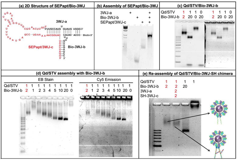
To confirm the resistive memory property of pRNA-3WJ/Qd chimera at nanoscale, the Qd/STV/Bio-3WJ-SH chimera was immobilized onto Au substrate at a dilute concentration. The electrical properties of Qd/STV/Bio-3WJ-SH chimera were examined by scanning tunneling spectroscopy(STS). To compare the electrical property of individual molecule, the thiol-modified pRNA-3WJ and Qd/STV was adsorbed onto Au substrate. I-V curves of each molecule were measured at room temperature by positioning the conductive tip on top of the sample. Figure 3a-d show STM and STS images of Au, thiol-modified pRNA-3WJ, Qd/STV, Qd/STV/Bio-3WJ-SH chimera. In case of the bare Au, only linear I-V characteristic (Ohmic behavior) was observed (Figure 3a). The bare Au substrate shows the general metallic conductor (linear) property. However, pRNA-3WJ-SH (Figure 3b) exhibits the non-linear I-V properties. Presumably, these biomolecules provide the energy band gap that makes the semiconducting behavior,39 and show the rectifying properties in the two-terminal system. Thus, it is hard to observe any resistive change effect in these molecules.
Figure 3. I-V plotting of the Qd/STV/Bio-3WJ-SH chimera on Au surface.
(a) Au surface, (b) Thiol-modified pRNA-3WJ on Au surface, (c) Qd/STV adsorbed on Au surface, (d) re-assembled Qd/STV/Bio-3WJ-SH chimera on Au surface.
| (1) |
When the Qd/STV was adsorbed onto Au surface, slight resistive-switching property was observed during the potential sweep (Figure 3c). It seems forming a double-tunnel junction configuration, such as Qd/STV/conducting Au substrate.
| (2) |
Although slight hysteresis is observed in the I-V curve of Qd/STV, which depends on various factors, such as donor-acceptor pair or Schottky barrier effects, but it mainly depends on the air gap between the tip and molecule.40 Even, the Qd/STV/Au system shows a little resistive switching property of the metal/molecule/metal tunneling junction, the On/Off ratio was very weak and fluctuating. So it is hard to use for resistive biomemory application.
However, the Qd/STV/Bio-3WJ-SH chimera shows the distinctive effect compared to Qd/STV. The electrical bipolar switching behavior was observed. Presumably, the observed electrical bistability of the conjugated Qd/STV/Bio-3WJ-SH chimera originated from the conjugation of pRNA-3WJ and Qd/STV rather than an electronic phenomenon caused by either one of the two nanomaterials composing the chimera.
| (3) |
As Figure 3d shows that resistive switching effect of Qd/STV/Bio-3WJ-SH chimera, the resistive switching effect can be observed when trace and retrace linear voltage scans applied from 0 to –3.0 V and –3.0 to 0 V, respectively. Initially, the I-V curve of chimera shows a low conductivity state and this state was defined as ‘OFF’. When the potential reaches about 1.8 V, where an abrupt increase in conductivity occurs, defines the as ‘ON’ state. This state indicates a transition of the chimera molecule from an initial OFF state to an ON state that is equivalent to the “writing” process in a digital resistive memory device. The high conductive state retained over 1.8 V. Thus, the threshold voltage (VTh) for switching is 1.8 V. When a negative voltage is applied continuously, the chimera molecule is retained the ON state until 0.3 V. Then, it returned to low conductivity state (OFF state). This reverse voltage state is equivalent to the “erase” process in the memory device. Moreover, additional experiments were carried out to analyze the characteristics of current-distance characteristics (I-s) (Supplemental Figure 2), and its derivatives (Supplemental Figure 3, Supplemental Table 1) are explained in the supplementary materials.
Resistive Biomemory Characteristics of the Qd/STV/Bio-3WJ-SH Hybrid
To investigate the resistive switching mechanism based on trap and release of charge, biomemory function was analyzed. Figure 4a describes the I-V characteristics of Qd/STV/Bio-3WJ-SH when a bias voltage is applied from +3 to -3 V. As shown in the figure the device starts switching to a conductive state (ON state) when the applied voltage is +1 V with a sharp increase in the current and remains in the state until the reverse voltage is applied. The device shows electrical hysteresis behavior which is an essential feature of bistable devices. State “1” and state “0” correspond to the relatively high-current (ON state) and the relatively low-current states (OFF state), respectively. The bistable transition from the “OFF” state to the “ON” state is equivalent to the “writing” process in a digital memory cell. After transition is achieved, the ON state remains in the device even after power is turned off. In presence of Qd/STV/Bio-3WJ-SH chimera system, the CdSe core in Qd and the pRNA-3WJ are separated by a large energy-gap ZnS semiconductor tunneling barrier. The pRNA-3WJ behaves as the charge donor during the conductivity switching allowing charge transfer to the lower-energy core.40-43 We assume that an electric field induced charge transfer mechanism between the polyanionic pRNA-3WJ and the Qd core is responsible for the observed electrical bistability of Qd/STV/Bio-3WJ-SH chimeras. Figure 4 shows a study on the conduction mechanism in both the ON and OFF states of the RNA-Qd chimera. To understand the conducting mechanism through the device, the I-V curves of this device in both states were analyzed in terms of theoretical models.
Figure 4. I-V characterization of the electrical bi-stability behavior.
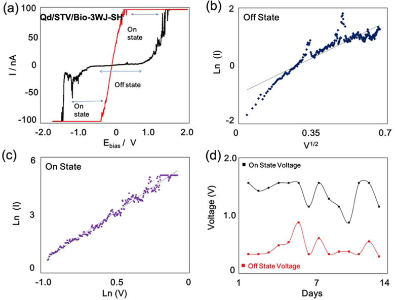
(a) I-V characteristics of the Qd/STVQd/STV/Bio-3WJ-SH chimera on Au, exhibiting electrical bi-stability behavior where the current transition from the low (OFF state) to high (ON state) and from low resistance state to high resistance showing the memory effect. (b) Plot of ln(I)-V1/2 fit for low conducting state which was attributed to thermionic emission (c) ln(I)-ln(V) fit for the high conductance state respectively. The magnitude of current and voltage have been plotted to show the reverse bias section of the characteristics. (d) Retention time and stability test of Qd/STV/Bio-3WJ-SH chimera on Au substrate.
The plot of log(I) as a function of V1/2 (Figure 4b) fitted to a straight line, which suggests that the conduction mechanism is probably due to thermionic emission. Therefore, the conduction mechanism in the low conductivity state is dominated by charge injection from the electrode to the pRNA-3WJ. A liner curve was obtained between log I and V1/2 (Figure 4b) from 0 to 0.7 V for the device in the OFF state. The I-V relationship in OFF state of Qd/STV/Bio-3WJ-SH chimera could be explained with the injection-dominated thermionic emission (IDTE) model.41 Accordingly, current density (J) at a particular filed F (=V/d) is given by
Where A is a constant, ϕ is the barrier with the electrode, e is the electronic charge, ε is the permittivity of the active material, and T is the temperature. In Figure 4b, the plot of ln (I) versus V1/2 was fitted to a linear model with mostly similar slopes, which aligns with the suggested model.41 The y-axis intercepts depends on the barrier height with the electrode. This suggests that the off current is controlled by charge injection from the Pt electrode which is due the difference in the energy levels. Thus, energy barrier between the Pt electrode and the Qd/STV/Bio-3WJ-SH layer, and the charge injection through the energy barrier dominates the conduction mechanism. It was varied with the active material in the biomemory device, for example, the streptavidin-coated ZnS shell thickness on CdSe or the pRNA-3WJ conjugated with the nanoparticles. This could be due to a decrease in the effective band gap of the core-shell nanoparticles that determines the barrier height with the electrode.
In case of the ON state, the I-V relationship is changed for pRNA-3WJ-Qd chimera which shows the Ohmic behavior, a linear relation was also observed from the plot of log(I) as a function of log(V) in the high conductivity state, as shown in Figure 4c. From this plot it can be observed that a space-charge limited conduction (SCLC) emission is likely to be the conduction mechanism in the high conductivity state. The current flows through a pRNA-3WJ-Qd chimera conduction path. The space charge limited current is given by Mott-Gurne law,10
where μ is the carrier mobility and d is the thickness.
The higher bias voltage helps overcome the high band gap ZnS cap potential barrier by tunneling and injects electrons into the CdSe core. When a threshold voltage is reached (i.e., 1.8 V), the applied potential enables tunneling into the CdSe core, causing a high conductance switch. Hysteresis was observed in return scanning from high to low bias, suggesting the presence of a small amount of charge storage in the Qd core. Increase in potential induced strong SCLC conduction because more injection carriers from electrode results in more accumulated carriers at interface between the electrode and RNA. Therefore, we can hypothesize that the current conduction changed from an injection dominated mechanism in low conductivity state to a charge-injection-dominated mechanism in the high conductivity state. It is assumed that the charge transfer process is the result of the charge donating ability of the RNA which enables the observed bi-stability behavior while it also provides a direct pathway to the charge transfer phenomenon. Therefore, a charge transport mechanism occurs during the transition between the conducting states. This proposed mechanism is similar to that of the devices using other materials, related to charge acceptor and donor behaviors of many bistable resistive memory devices.44,45
To confirm the stability of the pRNA-3WJ/Qd chimera for use as a resistive biomemory device, the retention time test of pRNA-3WJ/Qd chimera layer was conducted using STS experiment. The I-V curve of Qd/STV/Bio-3WJ-SH chimera measurement was conducted at room temperature (Figure 4d). The potential sweep cycles were applied to determine the write and erase voltages for the device ON and OFF states, respectively. The retention time test was continued to 13 days in air condition, after which the Qd/STV/Bio-3WJ-SH chimera interface was getting damaged and degraded through joule heating and contaminating the chimera molecule during the operation of the device.
Conclusion
In summary, we report the development of the pRNA-3WJ/Qd chimerical nanoparticle using RNA aptamer-based method for the resistive biomolecular memory application. The pRNA-3WJ motif was re-designed to introduce both the Sephdaex G100-recognized aptamer and the biotin strand. The Sephadex G100 aptamer based conjugation method provides a specific binding ratio between Qd/STV and Bio-3WJ. This unique bio-inorganic chimerical nanoparticle exhibits the electrical bi-stability at the nanoscale for the resistive biomolecular memory function and this electrical property was well retained for 13 days. The present study shows the use of Qd/STV/Bio-3WJ-SH chimera provides possibility of biomolecular electronic apparatus application. The Qd/STV/Bio-3WJ-SH chimera displayed potential for applications in next-generation nonvolatile nanobio electronic devices. In the near future, the RNA-inorganic chimera materials can be further developed into candidates for nanobioelectronic devices such as information storage device, logic gate, processing device, eventually, nanobio computing systems.
Materials And Methods
Materials
The grain-controlled ultraflat Au substrate (Platypus® Template Stripped Gold Chips) was purchased from Platypus Technologies (USA) for scanning tunneling microscopy (STM) and scanning tunneling spectroscopy (STS). Mica was purchased from Ted Pella (USA) for atomic force microscopy (AFM) experiment. After immobilization, the substrate was washed with diethylpyrocarbonate (DEPC) treated water(Sigma-Aldrich, USA) and then dried with N2 gas. The Streptavidin-Quantom Dots (CdSe-ZnS, 655 nm) nanoparticles were purchased from Life Technology (USA). The Sephadex G100 resin was purchased from Sigma Aldrich (USA). The binding buffer (50 mM HEPES, 150 mM NaCl, 10 mM MgCl2·6H2O) and the elution buffer (4 M Urea, 5mM EDTA) were prepared for conjugation. Milli-Q water (DDW >18 MΩ) was used for all experiments.
In vitro synthesis and purification of pRNA-3WJ
The pRNA-3WJ-a and 5′-end biotin-labeled pRNA-3WJ-b (Bio-3WJ-b), DNA 3WJ-b, 5′-end thiol-labeled pRNA-3WJ-c (SH-3WJ-c) were chemically synthesized by Integrated DNA Technologies (IDT, IOWA, USA) (see supplemental Table 1). A sephadex G100 binding RNA aptamer sequence was added to the 3′-end of pRNA-3WJ-c (Figure 2a).35 The Sephadex G100 RNA aptamer-3WJ-c (SEPapt-3WJ-c) was then synthesized by in vitro transcription of the corresponding DNA template by T7 RNA polymerase.12,36
Construction of pRNA-3WJ nanoparticle harboring Sephadex aptamer and Biotin
The pRNA-3WJ nanoparticle harboring Sephadex aptamer and biotin (SEPapt/Bio-3WJ) was assembled by annealing three corresponding RNA strands at equal molar ratio in TMS buffer (40 mM Tris-HCl, 10 mM MgCl2, 100 mM NaCl) by heating at 80°C for 5 min, followed by slowly cooling down to 4°C at a rate of 2°C/min on a Master cycle thermocycler (Eppendorf, Germany). The nanoparticle assembly was confirmed by 8% native polyacrylamide gel prepared in TBM buffer (89 mM Tris, 200 mM boric acid, 5 mM MgCl2, pH 7.6). About 0.2 ug of RNA samples were loaded into each lane. After running at 80 V in a 4°C for 2h, the RNA nanoparticles were visualized by fluorescence signal or ethidium bromide staining, with images captured by Typhoon FLA 7000(GE Healthcare, UK).
RNA aptamer-based conjugation between Qd/STV and Bio-3WJ
The RNA aptamer-based conjugation technique was carried out for the production of the pRNA-3WJ/Qd chimera (Figure 1a). The first step is to immobilize SEPapt/Bio-3WJ complex onto the Sephadex G100 resin through the aptamer recognition reaction. Simply, the SEPapt/Bio-3WJ complex (1 uM) were mixed with the Sephadex G100 Resin (50 mg) in binding buffer and incubated for 12 hrs at 4 °C with shaking. The SEPapt/Bio-3WJ complex immobilized to G100 resins were then washed three times by centrifugation with binding buffer. Then, 300 μl of 400 nM streptavidin-coated Qd (Qd/STV, CdSe/ZnS, 655 nm) was added with gentle shaking at 4 °C in dark for 6 hrs. The Qd/STV was bound to SEPapt/Bio-3WJ complex that immobilized on G100 resins through streptavidin and biotin interaction. Unreacted Qd/STV was washed out by centrifugation with binding buffer for three times. Finally, the Qd/STV/Bio-3WJ-b was released from G100 resins by adding elution buffer containing 4 M urea, 5 mM EDTA with gentle mixing for approximately 30 mins, this step was repeated 5 times to increase the recovery yield. Then, the Qd/STV/Bio-3WJ-b fragment and SEPapt/3WJ-c and DNA 3WJ-a fragments were dissociated in elution buffer to separate the Qd/STV/Bio-3WJ-b and other 3WJ fragments from G100 resins. The eluent containing Qd/STV/Bio-3WJ-b was purified using Amicon Ultra centrifugal filter (MWCO 10K, Millipore, USA). Qd/STV/Bio-3WJ-b was re-assembled into Qd/STV/Bio-3WJ-SH by incubating with 3WJ-a and SH-3WJ-c to acquire a final 3WJ/Qd nanoparticle with all three 3WJ-a-b-c fragments for further experiments.
Surface characterization for confirmation of Qd/STV/Bio-3WJ-SH chimera nanoparticles
To test the electrical property of SH-modified Qd/STV/Bio-3WJ-SH chimera at the nanoscale, the chimera samples were diluted to 2 nM in TMS buffer (50mM Tris, 100mM NaCl, 10mM MgCl2). The droplet of samples (10 μL) was immediately self-assembled on ultra-flat Au substrate through covalent bonding between SH-group and Au. After a 10 min incubation period on the specifically modified Au surface,36 excess samples were washed with DEPC treated water and dried under a flow of N2 gas. STM and STS measurements were performed on a Digital Instruments Multimode STM using a Nanoscope III controller (Veeco, CA, USA). Measurements were conducted under ambient conditions using mechanically cut Pt tips.
Electrical measurements of Qd/STV/Bio-3WJ-SH chimera nanoparticles
For I-V measurements, the STM tip was located above the spot to be measured. No additional force was applied to the tip and the same set point of 0.5 nA with a bias voltage of 0.1 V was used for all experiments. All the electrical measurements on single Qd/STV/Bio-3WJ-SH chimera were performed by STM under an open air environment at ambient conditions. The tunneling current was observed as the tip-sample bias was ramped in the range of ± 3 V. The shape of the I-V curve depends on the STM tip position over the Qd/STV/Bio-3WJ-SH chimera where the current is measured. In a typical electrical characterization experiment, a “point and shoot” method was used to directly place the STM tip (Pt/Ir) on a single Qd/STV/Bio-3WJ-SH chimera. All measurements were carried out by first taking a morphology scan of an individual molecule of assembled Qd/STV/Bio-3WJ-SH chimera. Then the STM tip was positioned to the top of a single Qd/STV/Bio-3WJ-SH chimera. For the purpose of the electrical characterization at the nanoscale, the ultraflat Au substrate (Platypus® Template Stripped Gold Chips) was used as the bottom electrode while the 14 mm length of the conductive STM tip was used as the top electrode for the two-terminal system.
Supplementary Material
Acknowledgments
The authors would like to thank M. Vieweger for comments on the project. This research was supported by Leading Foreign Research Institute Recruitment Program through the National Research Foundation of Korea (NRF) funded by the Ministry of Science, ICT & Future Planning (MSIP) (2013K1A4A3055268), and NIH grants U01CA151648 486 and R01EB012135 to P.Guo. Funding to P. Guo's Endowed Chair in Nanobiotechnology position is by the William Fairish Endowment Fund. P. Guo is a co-founder of Biomotor and RNA Nanotechnology Development Corp. Ltd.
Footnotes
Supporting Information Available: The surface investigation of pRNA 3WJ, Qd/STV, Qd/STV/Bio-3WJ-SH conjugate by STM, and current-distance characteristics of the Qd/STV/Bio-3WJ-SH hybrid nanoparticles. These materials are available free of charge via the internet at http://pubs.acs.org
Reference List
- 1.Moore GE. Cramming More Components Onto Integrated Circuits (Reprinted From Electronics, Pg 114-117, April 19, 1965) Proc IEEE. 1998;86:82–85. [Google Scholar]
- 2.Petty MC. Scope of Molecular Electronics. In: Petty MC, editor. Molecular Electronics: From Principles to Practice. 1st. Wiley; West Sussex; 2008. [Google Scholar]
- 3.Kim TW, Lee K, Oh SH, Wang G, Kim DY, Jung GY, Lee T. A Direct Metal Transfer Method for Cross-Bar Type Polymer Non-Volatile Memory Applications. Nanotechnology. 2008;19 doi: 10.1088/0957-4484/19/40/405201. [DOI] [PubMed] [Google Scholar]
- 4.Heath JR. Molecular Electronics. Annu Rev Mater Res. 2009;39:1–23. [Google Scholar]
- 5.Lu W, Lieber CM. Nanoelectronics From the Bottom Up. Nat Mater. 2007;6:841–850. doi: 10.1038/nmat2028. [DOI] [PubMed] [Google Scholar]
- 6.Tseng RJ, Tsai CL, Ma LP, Ouyang JY. Digital Memory Device Based on Tobacco Mosaic Virus Conjugated With Nanoparticles. Nat Nanotechnol. 2006;1:72–77. doi: 10.1038/nnano.2006.55. [DOI] [PubMed] [Google Scholar]
- 7.Offenhausser A, Rinaldi R. Nanobioelectronics - for Electronics, Biology, and Medicine. Springer; New York: 2009. [Google Scholar]
- 8.Noy A. Bionanoelectronics. Adv Mater (Weinheim, Ger) 2011;23:807–820. doi: 10.1002/adma.201003751. [DOI] [PubMed] [Google Scholar]
- 9.Cho B, Song S, Ji Y, Kim TW, Lee T. Organic Resistive Memory Devices: Performance Enhancement, Integration, and Advanced Architectures. Adv Funct Mater. 2011;21:2806–2829. [Google Scholar]
- 10.Ko Y, Kim Y, Baek H, Cho J. Electrically Bistable Properties of Layer-by-Layer Assembled Multilayers Based on Protein Nanoparticles. ACS Nano. 2011;5:9918–9926. doi: 10.1021/nn2036939. [DOI] [PubMed] [Google Scholar]
- 11.Strukov DB, Kohlstedt H. Resistive Switching Phenomena in Thin Films: Materials, Devices, and Applications. MRS Bull. 2012;37:108–117. [Google Scholar]
- 12.Guo P. The Emerging Field of RNA Nanotechnology. Nat Nanotechnol. 2010;5:833–842. doi: 10.1038/nnano.2010.231. [DOI] [PMC free article] [PubMed] [Google Scholar]
- 13.Shu D, Shu Y, Haque F, Abdelmawla S, Guo P. Thermodynamically Stable RNA Three-Way Junctions for Constructing Multifuntional Nanoparticles for Delivery of Therapeutics. Nat Nanotechnol. 2011;6:658–667. doi: 10.1038/nnano.2011.105. [DOI] [PMC free article] [PubMed] [Google Scholar]
- 14.Guo P, Zhang C, Chen C, Trottier M, Garver K. Inter-RNA Interaction of Phage Phi29 PRNA to Form a Hexameric Complex for Viral DNA Transportation. Mol Cell. 1998;2:149–155. doi: 10.1016/s1097-2765(00)80124-0. [DOI] [PubMed] [Google Scholar]
- 15.Guo P, Erickson S, Anderson D. A Small Viral RNA Is Required for in Vitro Packaging of Bacteriophage Phi29 DNA. Science. 1987;236:690–694. doi: 10.1126/science.3107124. [DOI] [PubMed] [Google Scholar]
- 16.Shu Y, Haque F, Shu D, Li W, Zhu Z, Kotb M, Lyubchenko Y, Guo P. Fabrication of 14 Different RNA Nanoparticles for Specific Tumor Targeting Without Accumulation in Normal Organs. RNA. 2013;19:766–777. doi: 10.1261/rna.037002.112. [DOI] [PMC free article] [PubMed] [Google Scholar]
- 17.Shu D, Moll WD, Deng Z, Mao C, Guo P. Bottom-Up Assembly of RNA Arrays and Superstructures As Potential Parts in Nanotechnology. Nano Lett. 2004;4:1717–1723. doi: 10.1021/nl0494497. [DOI] [PMC free article] [PubMed] [Google Scholar]
- 18.Shu Y, Shu D, Haque F, Guo P. Fabrication of PRNA Nanoparticles to Deliver Therapeutic RNAs and Bioactive Compounds into Tumor Cells. Nat Protoc. 2013;8:1635–1659. doi: 10.1038/nprot.2013.097. [DOI] [PMC free article] [PubMed] [Google Scholar]
- 19.Binzel DW, Khisamutdinov EF, Guo P. Entropy-Driven One-Step Formation of Phi29 PRNA 3WJ From Three RNA Fragments. Biochemistry. 2014;53:2221–2231. doi: 10.1021/bi4017022. [DOI] [PMC free article] [PubMed] [Google Scholar]
- 20.Haque F, Shu D, Shu Y, Shlyakhtenko L, Rychahou P, Evers M, Guo P. Ultrastable Synergistic Tetravalent RNA Nanoparticles for Targeting to Cancers. Nano Today. 2012;7:245–257. doi: 10.1016/j.nantod.2012.06.010. [DOI] [PMC free article] [PubMed] [Google Scholar]
- 21.Liu J, Guo S, Cinier M, Shlyakhtenko LS, Shu Y, Chen C, Shen G, Guo P. Fabrication of Stable and RNase-Resistant RNA Nanoparticles Active in Gearing the Nanomotors for Viral DNA Packaging. ACS Nano. 2011;5:237–246. doi: 10.1021/nn1024658. [DOI] [PMC free article] [PubMed] [Google Scholar]
- 22.Khisamutdinov EF, Jasinski DL, Guo P. RNA As a Boiling-Resistant Anionic Polymer Material to Build Robust Structures With Defined Shape and Stoichiometry. ACS Nano. 2014;8:4771–4781. doi: 10.1021/nn5006254. [DOI] [PMC free article] [PubMed] [Google Scholar]
- 23.Khisamutdinov E, Li H, Jasinski D, Chen J, Fu J, Guo P. Enhancing Immunomodulation on Innate Immunity by Shape Transition Among RNA Triangle, Square, and Pentagon Nanovehicles. Nucleic Acids Res. 2014;42:9996–10004. doi: 10.1093/nar/gku516. [DOI] [PMC free article] [PubMed] [Google Scholar]
- 24.Chworos A, Severcan I, Koyfman AY, Weinkam P, Oroudjev E, Hansma HG, Jaeger L. Building Programmable Jigsaw Puzzles With RNA. Science. 2004;306:2068–2072. doi: 10.1126/science.1104686. [DOI] [PubMed] [Google Scholar]
- 25.Afonin KA, Viard M, Koyfman AY, Martins AN, Kasprzak WK, Panigaj M, Desai R, Santhanam A, Grabow WW, Jaeger L, Heldman E, Reiser J, Chiu W, Freed EO, Shapiro BA. Multifunctional RNA Nanoparticles. Nano Lett. 2014;14:5662–5671. doi: 10.1021/nl502385k. [DOI] [PMC free article] [PubMed] [Google Scholar]
- 26.Lee JB, Hong J, Bonner DK, Poon Z, Hammond PT. Self-Assembled RNA Interference Microsponges for Efficient SiRNA Delivery. Nat Mater. 2012;11:316–322. doi: 10.1038/nmat3253. [DOI] [PMC free article] [PubMed] [Google Scholar]
- 27.Stephenson W, sare-Okai PN, Chen AA, Keller S, Santiago R, Tenenbaum SA, Garcia AE, Fabris D, Li PT. The Essential Role of Stacking Adenines in a Two-Base-Pair RNA Kissing Complex. J Am Chem Soc. 2013;135:5602–5611. doi: 10.1021/ja310820h. [DOI] [PMC free article] [PubMed] [Google Scholar]
- 28.Leontis NB, Westhof E. Self-Assembled RNA Nanostructures. Science. 2014;345:732–733. doi: 10.1126/science.1257989. Chemistry. [DOI] [PubMed] [Google Scholar]
- 29.Hsu BB, Hagerman SR, Jamieson K, Veselinovic J, O'Neill N, Holler E, Ljubimova JY, Hammond PT. Multilayer Films Assembled From Naturally-Derived Materials for Controlled Protein Release. Biomacromolecules. 2014;15:2049–2057. doi: 10.1021/bm5001839. [DOI] [PMC free article] [PubMed] [Google Scholar]
- 30.Sun H, Sheng J, Hassan AE, Jiang S, Gan J, Huang Z. Novel RNA Base Pair With Higher Specificity Using Single Selenium Atom. Nucleic Acids Res. 2012;40:5171–5179. doi: 10.1093/nar/gks010. [DOI] [PMC free article] [PubMed] [Google Scholar]
- 31.Shopsowitz KE, Roh YH, Deng ZJ, Morton SW, Hammond PT. RNAi-Microsponges Form Through Self-Assembly of the Organic and Inorganic Products of Transcription. Small. 2014;10:1623–1633. doi: 10.1002/smll.201302676. [DOI] [PMC free article] [PubMed] [Google Scholar]
- 32.Westhof E. Isostericity and Tautomerism of Base Pairs in Nucleic Acids. FEBS Lett. 2014;588:2464–2469. doi: 10.1016/j.febslet.2014.06.031. [DOI] [PubMed] [Google Scholar]
- 33.Moll D, Guo P. Grouping of Ferritin and Gold Nanoparticles Conjugated to PRNA of the Phage Phi29 DNA-Packaging Motor. J Nanosci Nanotechnol. 2007;7:3257–3267. doi: 10.1166/jnn.2007.914. [DOI] [PubMed] [Google Scholar]
- 34.Jung D, Minami I, Patel S, Lee J, Jiang B, Yuan Q, Li L, Kobayashi S, Chen Y, Lee KB, Nakatsuji N. Incorporation of Functionalized Gold Nanoparticles into Nanofibers for Enhanced Attachment and Differentiation of Mammalian Cells. J Nanobiotechnology. 2012;10:23. doi: 10.1186/1477-3155-10-23. [DOI] [PMC free article] [PubMed] [Google Scholar]
- 35.Srisawat C, Goldstein I, Engelke D. Sephadex-Binding RNA Ligands: Rapid Affinity Purification of RNA From Complex RNA Mixtures. Nucleic Acids Res. 2001;29:E4. doi: 10.1093/nar/29.2.e4. [DOI] [PMC free article] [PubMed] [Google Scholar]
- 36.Jasinski D, Khisamutdinov EF, Lyubchenko YL, Guo P. Physicochemically Tunable Poly- Functionalized RNA Square Architecture With Fluorogenic and Ribozymatic Properties. ACS Nano. 2014;8:7620–7629. doi: 10.1021/nn502160s. [DOI] [PMC free article] [PubMed] [Google Scholar]
- 37.Ponchon L, Dardel F. Recombinant RNA Technology: the TRNA Scaffold. Nat Methods. 2007;4(7):571–576. doi: 10.1038/nmeth1058. [DOI] [PubMed] [Google Scholar]
- 38.Ponchon L, Dardel F. Large Scale Expression and Purification of Recombinant RNA in Escherichia Coli. Methods. 2011;54:267–273. doi: 10.1016/j.ymeth.2011.02.007. [DOI] [PubMed] [Google Scholar]
- 39.Smith AM, Nie S. Semiconductor Nanocrystals: Structure, Properties, and Band Gap Engineering. Acc Chem Res. 2010;43:190–200. doi: 10.1021/ar9001069. [DOI] [PMC free article] [PubMed] [Google Scholar]
- 40.Jortner J, Bixon M, Langenbacher T, Michel-Beyerle ME. Charge Transfer and Transport in DNA. Proc Natl Acad Sci U S A. 1998;95:12759–12765. doi: 10.1073/pnas.95.22.12759. [DOI] [PMC free article] [PubMed] [Google Scholar]
- 41.Chu CW, Ouyang J, Tseng HH, Yang Y. Organic Donor-Acceptor System Exhibiting Electrical Bistability for Use in Memory Devices. Adv Mater (Weinheim, Ger) 2005;17:1440–1443. doi: 10.1002/adma.200500225. [DOI] [PubMed] [Google Scholar]
- 42.Voityuk AA. Electronic Coupling for Charge Transfer in Donor-Bridge-Acceptor Systems. Performance of the Two-State FCD Model. Phys Chem Chem Phys. 2012;14:13789–13793. doi: 10.1039/c2cp40579b. [DOI] [PubMed] [Google Scholar]
- 43.Zhang Y, Zherebetskyy D, Bronstein ND, Barja S, Lichtenstein L, Schuppisser D, Wang LW, Alivisatos AP, Salmeron M. Charge Percolation Pathways Guided by Defects in Quantum Dot Solids. Nano Lett. 2015 doi: 10.1021/acs.nanolett.5b00454. [DOI] [PubMed] [Google Scholar]
- 44.Kim TW, Yang Y, Li FS, Kwan WL. Electrical Memory Devices Based on Inorganic/Organic Nanocomposites. NPG Asia Mater. 2012;4 [Google Scholar]
- 45.Ribierre JC, Aoyama T, Muto T, Andre P. Hybrid Organic-Inorganic Liquid Bistable Memory Devices. Org Electron. 2011;12:1800–1805. [Google Scholar]
Associated Data
This section collects any data citations, data availability statements, or supplementary materials included in this article.