Abstract
Here, we quantify for the first time the operating conditions of a 3-terminal magnetophoretic transistor architecture used to switch magnetically labeled single cells and single magnetic beads along different paths in microfluidic environments. The semiconducting transport properties are achieved by engineering a small gap between two magnetic disks. Cell and bead motion across the gap is controlled by the gate currents from nearby microwires, which produce competing magnetic fields to toggle the locations of the magnetic potential energy minima. We demonstrate both attractive and repulsive transistor modes, in which cells transfer towards the microwire (attractive mode) or away from microwire (repulsive mode). This novel two-way switching capability allows cells to be written to, or extracted from, specified storage areas in a multiplexed array. For both attractive and repulsive modes, we find that complete switching is achieved with as little as 10–20 mA gate currents in 0–100 Oe static and dynamic external magnetic fields. When combined with a non-fouling brush grafted to the chip surface to reduce non-specific cell adhesion, this platform opens the door to scalable, biologically relevant applications and multiplexing of large single cell arrays.
Keywords: single cell, magnetism, microfabrication, microfluidics, transistor
Single cell arrays are an increasingly important tool for biology[1–10]; however most existing single cell platforms are unable to perform large-scale operations on single cells with the flexibility and automation of modern day computer circuits. Inspired by the random access memory architecture (RAM), we developed a novel approach for logic-based transport of single cells in microfluidic environments[11]. This approach uses passive circuit elements (conductors, capacitors, and diodes) to transport single cell to pre-designated switching junctions. Active circuit elements (transistors and multiplexers) are used to switch the direction of cells at junctions, enabling their individual isolation, multiplexing, and retrieval from the array. The switching thresholds of previous transistor architectures, however, have yet to be experimentally quantified. Moreover, prior systems lacked reciprocal writing capabilities (i.e., ability to import a cell into, and export a cell out of, an array site). Finally, surfactants were required to prevent adhesion of particles and cells to the chip surface, which limited its capability for extended cell cultures.
Here, we experimentally quantify for the first time the switching thresholds of a general 3-terminal magnetophoretic transistor. Our efforts to optimize the device for low-power consumption, along with the development of novel biocompatible surface coatings, have enabled a novel platform which can be scaled to address biologically relevant problems in single cell analysis.
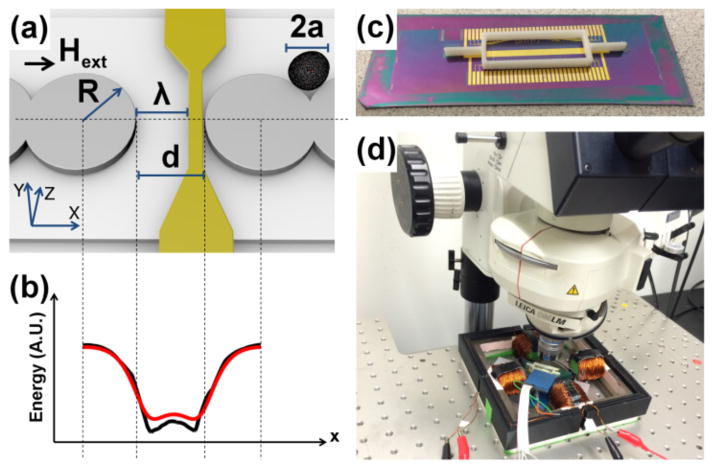
The magnetophoretic transistor device has strong parallels with the electronic bandgaps of conventional 3-terminal transistor switches. We create a semiconduting region for cell transport by introducing a small gap between two magnetizable disks (Figure 1a–b). This gap prevents the crossing of single cells and beads, except in the presence of an external gate bias. The transport properties can be understood through the space-time variations in the magnetic potential energy landscape. The energy is determined by computing the local magnetic field distribution B⃗(r⃗), and by assuming that the beads and cells behave like point dipoles with magnetic moments m⃗ = χVB⃗/μ0,, where V is the volume, χ is the volumetric magnetic susceptibility, and μ0 is the magnetic permeability of vacuum. The energy landscape in the horizontal plane located at one cell radius above the substrate is calculated from: U = −½m⃗·B⃗. As shown in Figure 1(a–b), a double-well potential appears in the absence of a gate current, in which an energy barrier is observed at the center of the gap. (See Figure 1a–b). This energy barrier prevents spontaneous cell and bed motion across the gap in the unactuated state. However, if the magnetic field is locally tuned by an adjacent microwire (gold wire of Figure 1a), then the double well potential merges into a single energy minimum, allowing the cells to be transferred across the gap. The gate current threshold required to activate particle transport across the gap is similar to the band referenced Fermi level of semiconductors. The direction of particle crossing (towards or away from the microwire) can be controlled with the field orientation and the direction of the applied gate current.
Figure 1. Illustration of the transistor geometry and potential energy distribution.
(a) Ni81Fe19 permalloy disks (gray circles) of radius, R, and thickness, τm are designed with a small gap of distance, d. A gate electrode (gold wire) is overlaid with its left edge shifted from the opposing gap side by a distance, λ. A magnetized cell (black circle) of radius, a, is shown moving along the magnetic track. The external field direction, Hext, is aligned along the track axis, depicted as the black arrow. The potential energy line cross-section simulated at a vertical height of z = a is shown in (b) from finite element (FEM) analysis (black line), and from analytical charge model (red line) based on Eqs. 1–2. A photograph of the chip and 3D printed container used to test the transistors are shown in (c). The overall instrument apparatus is shown in (d).
We designed, optimized, and built magnetophoretic transistors from aligned layers of magnetic permalloy disk patterns and gold wire patterns. These devices were fabricated on silicon wafers (University Wafer, Boston, MA) by conventional photolithographic lift-off technique. The magnetic pattern consisted of a 5nm/100nm stack of Ti/Ni81Fe19. The overlaid microwire patterns consisted of a 5nm/100nm stack of Ti/Au. In between each metallic layer and on the top and bottom surfaces, we deposited 250nm of SiO2 by PECVD (Advanced Vacuum Vision 310) in order to electrically isolate the gate electrodes from the magnetic layer and fluid. More information on the processing conditions and experimental testing protocol is provided in the Supplementary Materials and Methods.
The transistor geometry consists of permalloy disks with radius, R, and thickness, τm, and are separated by a gap of distance, d at the switching junction. A metallic wire of thickness τw, is overlaid with its left edge shifted by a distance, λ, from the disk edge on the opposing side of the gap. Locally strong magnetic fields are created by narrowing the wire to a width, rw, at the junction. Magnetically labeled cells are depicted by the black circle, having a mean radius, a.
We used finite element simulations (Ansys, Maxwell 15.0) to compute the magnetic fields in the gap between two disks, when in the presence of a uniform magnetic field applied along the track axis (x-direction). The equivalent magnetic charge distribution was evaluated on the disk surface using the relation: σ = (H⃗in − H⃗out)·n̂. The charge density on the axial surfaces and the perimeter are denoted by σs, and σp, respectively. Their geometric variations were found to correspond to hyberbolic and periodic functions as:
| (1a) |
| (1b) |
where the best fitting parameters were found to be σ0p = 6.2Hext, σ0s = 0.12Hext and γ = 4.
Once the charge distributions are determined, the magnetic potential φm is calculated by integrating over these charged surfaces:
| (2) |
The fields and field gradients produced by the disks are then calculated by taking successive derivatives of the magnetic potential[13], which allows for computation of the magnetic forces and potential energies. This method was used to produce energy line cross-sections (red line), which are in good agreement with the FEM based results (black line, Figure 1b). The energy surface cross-sections at one cell radius above the substrate are also shown in Figure 2, where the blue regions denote the local energy minima. The magnetic field from the gate electrode is calculated with the Biot-Savart law, assuming an infinitely thin sheet current:
| (3) |
where the wire’s field is assumed to be produced by a sheet current, K⃗(r⃗s) which is a reasonable approximation when the wire thickness (~100–200nm) is much smaller than the minimum planar dimensions of the wire (~2–3μm). In order to simplify our theoretical model, we assumed that the fields from the wire and magnetic disks are non-interacting. These assumptions were deemed necessary for computational efficiency to analyze switching properties and particle trajectories.
Figure 2. Transistor operational modes and their energy landscapes.
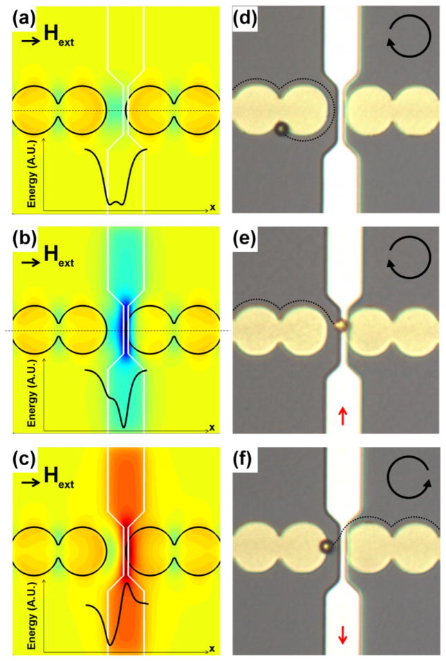
Magnetic potential energy landscapes are shown in (a–c) with corresponding experiments shown in (d–f). In (a–c), the line cross-sections are shown when no gate current is applied (a), in the attractive mode (b), and in the repulsive mode (c). In all cases, a constant uniform magnetic field is applied along the positive x-direction and denoted by the black arrow. In part (d), the bead remains on the same side of the gap due to the double well potential of part (a). In a clockwise rotating field (e), the bead moves across the gap towards the wire due to a gate current in the positive y-direction. In a counter-clockwise rotating field (f), the bead crosses the gap and moves away from the wire due to a gate current in the negative y-direction. Field rotation sense is denoted by the circular arrows, and gate currents are shown as red arrows.
One of the important challenges we faced stems from the tendency of cells to avidly adhere to untreated surfaces. Non-specific cell adhesion hinders controlled manipulation and must be solved for proper functioning of these multiplexed devices. To address this limitation, we deposited a “non-fouling” — protein and cell resistant— poly(oligoethylene glycol methyl methacrylate) (POEGMA) 50nm thick coating on top of the chip surface that reduced cell adhesion to the substrate. POEGMA surfaces were deposited by surface-initiated atom transfer radical polymerization (SI-ATRP). The approach has been previously described[14], but has never been attempted on lithographically patterned substrates. Briefly, the POEGMA layer was constructed by first functionalizing the SiO2 top surface of the chip with ATRP initiator and then immersing the substrates in polymerization solution, producing surface-tethered brushes of POEGMA. In order to protect the exposed electrodes and connectors, a 3D-printed chamber was then fastened on the chip with Silicone adhesive, shown in Figure 1c.
Magnetic beads (Spherotech CM 50–10) with mean diameters of 5.7-μm were used to test the transistor performance in deionized water. Magnetically labeled human CD4+ T-cells of a similar size range were also tested by conjugation to anti-CD4 antibody labeled magnetic nanoparticles (StemCell Technologies, Vancouver, Canada). The labeling efficiency and cell isolation purity were confirmed by flow cytometry. We developed a custom stage to perform microscopy, while also allowing for the application of rotating magnetic field. This stage, shown in Figure 1d, consists of a 4-pole iron plate (McMaster Carr) wrapped with magnet wire (20AWG), and powered by programmable power supplies (Kepco BOP 20-5M). We made electrical contact to the gate electrodes with IC test clips (Ponoma). Both the rotating fields and gate currents were controlled by customized LabVIEW programs (National Instrument), and the transport experiments were monitored in a Leica DM LM microscope using a Retiga 2000R video camera (Figure 1d).
We investigated two types of transistor modes, including an attractive mode, shown in Figure 2(b,e), and a repulsive mode shown in Figure 2(c,f). The energy landscapes of each of these modes in the presence and absence of gate currents are shown in Figure 2(a–c). Sufficiently strong gate currents can annihilate the double well energy barrier of Fig. 2a, and induce the cell to transfer across the gap towards the wire (attractive mode) or away from the wire (repulsive mode). Example particle trajectories for each transistor mode are provided in Figure 2(d–f), where the corresponding external field directions and in-plane rotating fields are also illustrated.
We measured the switching thresholds of the attractive and repulsive transistor modes through a combination of static and dynamic transistor tests, with the results shown in Figures 3 and 4. From simulations, we expected that optimal transistor performance can be achieved when the gap distance is similar to the cell diameter.[12] To test this hypothesis, we fabricated a series of transistors with gap distances ranging from 5–15μm to cover a range of dimensions relative to the typical diameters of human T-cells (6–10μm). For transistors gaps smaller than 8μm, we observed a high frequency of particle crossings in the absence of a gate current, rendering this geometry unsuitable for a transistor switch. For transistors gaps larger than 10μm, we found that excessively large gate currents were required to achieve reliable switching. The rest of this analysis thus focused on gap dimensions of 8μm or 10μm, which is slightly larger than the average cell diameter.
Figure 3. Transistor switching thresholds are depicted for magnetic beads.
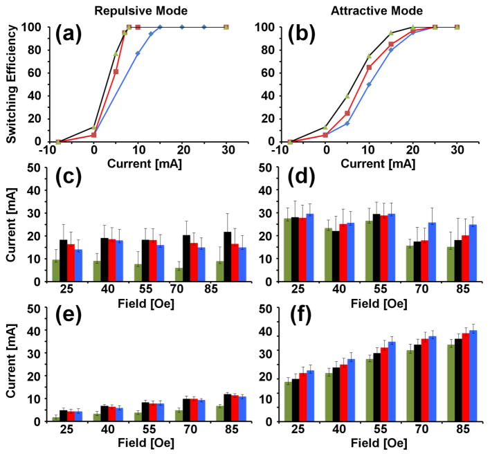
The experimental switching efficiency in the dynamic transistor tests is shown for the repulsive mode (a) and attractive mode (b) for driving frequencies of 0.2 Hz (blue), 0.5 Hz (red), and 0.8 Hz (black). In these dynamic tests, the rotating field magnitude is Hext=45Oe. The experimental switching thresholds in the static transistor tests for the repulsive mode (c) and attractive mode (d) are shown for device geometries of d=8μm and λ=6.5μm (green bars), d=10μm and λ=7μm (black bars), d=10μm and λ=8μm (red bars), d=10μm and λ=9μm (blue bars). Theoretical results presented in (e,f), correspond to the transistor mode types of (c,d) respectively.
Figure 4. Transistor switching efficiency for magnetically labeled T-cells.
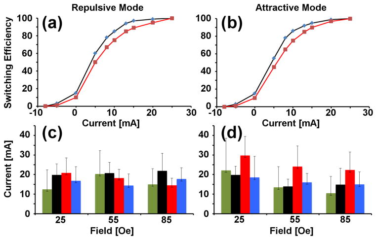
The experimental switching efficiency of magnetically labeled T-cells in the dynamic transistor tests is shown for the repulsive mode (a) and attractive mode (b) for driving frequencies of 0.2 Hz (blue), 0.5 Hz (red) in a constant 45Oe rotating magnetic field. The switching thresholds for cells in the static transistor tests for the repulsive mode (c) and attractive mode (d) are shown for device geometries of d=8μm and λ =6.5μm (green), d=10μm and λ=7μm (black), d=10μm and λ=8μm (red), d=10μm and λ=9μm (blue).
We investigated two approaches for evaluating the transistor performance, referred to as “static” and “dynamic” transistor tests. In the static test, we positioned the cells or beads at the gap junction, and then aligned the external field along the track axis (x-direction). Next, we slowly increased the gate current, and recorded hysteresis loops for the position vs. current, and in the process identified the gate currents when the cells and beads transferred across the gap (See supplementary movies S1 for beads and S2 for cells). The switching experiments were conducted on at least 10 beads or cells for each experimental condition, and we repeated the experiment in triplicate for each specific bead or cell. The average switching current thresholds for the attractive and repulsive transistor modes for magnetic beads and cells, respectively, are shown in the bar plots of Figure 3(c–d) and Figure 4(c–d).
In order to compare these experimental results with our theroetical model, we computed the expected current switching thresholds, assuming that the bead diameter was a random variable, with mean and standard deviation of 5.72 ± 0.86μm, as derived from pixel analysis based size measurments of a population of 30 magnetic beads. The simulation results and their standard deviations for the switching thresholds are provided in Figure 3(e–f), and used for comparison with experiments on magnetic beads. Simulations for cells show similar trends (data not shown).
In the barplots of Figures 3 and 4, each bar corresponds to a specific transistor geometry with a unique gap size and gate location. The black, red, and blue bars correspond to transistors with a gap size of 10μm, but with different offsets for the wire displacement from the disk edge, ranging from 7 to 9μm. The green bars of Figures 3 and 4 correspond to transistors with a smaller gap size of 8μm and a displacement of the microwire by 6.5μm from the gap center. In all cases, the wire width kept fixed at 3μm, which is the smallest photolithographically reproducible dimension.
Though there are some differences between theory and experiment, the simulations results predict the correct order of magnitude of the required switching currents, shown to be in the range of 10 – 30 mA. Experiments also confirmed our predictions that magnetic beads will switch at lower current threshold when the gap size is smaller. This trend is clearly observed in the repulsive transistor modes of Figure 3(c & e); however the trend still appears to be consistent for the attractive transistor modes and for the cell based switching experiments of Figure 4. Some features predicted in the theory were not observed in experiment, which are attributed to the oversimplifying assumptions in our idealized theoretical model. Improving the simulation accuracy would require better knowledge of the magnetic domain structure in the disk patterns as a function of the applied magnetic field, as well as more rigorous treatment of the field distribution using finite element models.
We next employed dynamic testing of the transistor switching efficiency, which is more representative of the device operating conditions. Using the transistor geometry of d=10μm and =9μm, the number of successful bead and cell crossings were monitored as a function of the applied gate currents in an externally applied 45Oe rotating magnetic field. The switching efficiency is also shown as a function of frequency for single beads in Figure 3(a–b) and for single cells in Figure 4(a–b). The motion of the beads and cells in the dynamic transistor tests are also shown in Supplementary Movies S3 and S4.
In comparing the data for the static and dynamic tests, we found that at low frequencies the switching thresholds were commensurate, which validates the simpler static tests to quantify transistor performance. At higher frequencies, the switching thresholds are reduced, as previously predicted[12], and thus frequency can be used as an additional control parameter to reduce the switching thresholds. For the magnetic beads in the repulsive mode (Figure 3a), we observe complete switching with gate currents of ~8mA for the 0.5Hz and 0.8Hz driving frequencies. On the other hand, complete switching is achieved with gate currents of ~15mA when the driving frequency is 0.2Hz, which is consistent with the static transistor tests. For the cell data, we find that complete switching is achieved at gate currents of ~20–25 mA for the 0.2 Hz and 0.5 Hz driving frequencies, which is also consistent with the static transistor tests.
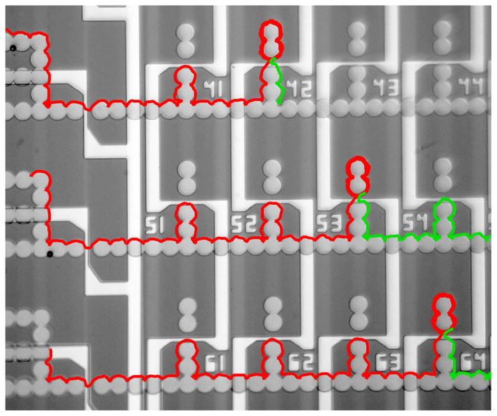
The ability to achieve both attractive and repulsive modes in a single transistor architecture allows us to implement the full write cycle (i.e., writing a bead or cell to the array, and extracting it from the array). These dual functions are depicted in Figure 5, where the red lines show the trajectories of magnetic beads written to array sites, and the green lines show the trajectories of beads retrieved from array sites. In total, this demonstration required 9 synchronized switch operations – 3 row switches were activated to introduce cells down specific rows in the array, while 3 column switches were activated in the repulsive and attractive mode, in order to introduce or retrieve the beads, respectively, from their designated storage sites. The actual trajectories are shown in Supplementary Movie S5, and an additional high resolution Movie S6 demonstrates that similar operations can be performed on magnetized cells.
Figure 5. Multiplexed arrays.
An 8×8 array was designed and built to import, store, and export magnetized objects. A small section of the array is shown here, in which 3 beads are temporarily stored in array sites 42, 53, and 64 with the import trajectories shown in red. At a later time, the beads are exported from these storage sites with the trajectoreis shown in green. The full trajectories can be found in Supplementary Movie S5.
The use of passive circuit elements (magnetic tracks) to transport magnetized objects in parallel with an external rotating magnetic field, in combination with active circuit elements (transistors) to switch objects at specific junctions, provides a scalability that is similar to that found in a computer RAM memory. As such, this platform avoids potential issues with localized heating and high power densities of nDEP and optical systems [15–20] and allows large numbers of objects to be controlled with relatively few gate electrodes. Our experimental quantification of the switching thresholds in 3-terminal magnetophretic transistor devices thus establishes the baseline for future efforts to scale this tool into a novel, biologically relevant platform for single cell analysis.
Supplementary Material
Acknowledgments
The authors are thankful to Cheol Gi Kim, of DGIST, Daegu, South Korea, for helpful discussions, and to Hamidreza Toroghi for providing the illustration in Figure 1a. This research was supported by the Creative and Novel Ideas in HIV Research Program (CNIHR) through a supplement to the University of Alabama at Birmingham (UAB) Center For AIDS Research funding (P30 AI027767). This funding was made possible by collaborative efforts of the Office of AIDS Research, the National Institutes of Allergies and Infectious Diseases, and the International AIDS Society. This study was also supported by NIH grant (1R56AI112360) and by the Duke University CFAR, an NIH funded program (5P30 AI064518).
References
- 1.Navin NE. Genome Biol. 2014;15:452. doi: 10.1186/s13059-014-0452-9. [DOI] [PMC free article] [PubMed] [Google Scholar]
- 2.MA Ch, Fan R, Ahmad H, Shi Q, Comin-Anduix B, Chodon Th, Koya RC, Liu Ch, Kwong GA, Radu CG, Ribas A, Heath JR. Nat Med. 2011;17:738. doi: 10.1038/nm.2375. [DOI] [PMC free article] [PubMed] [Google Scholar]
- 3.Kim J, Taylor D, Agrawal N, Wang H, Kim H, Han A, Rege K, Jayaraman A. Lab Chip. 2012;10:1813. doi: 10.1039/c2lc21202a. [DOI] [PubMed] [Google Scholar]
- 4.Mullard A. Nat Rev Drug Discovery. 2011;10:477. doi: 10.1038/nrd3487. [DOI] [PubMed] [Google Scholar]
- 5.Chattopadhyay PK, Gierahn TM, Roederer M, Love JCh. Nat Immunol. 2014;15:128. doi: 10.1038/ni.2796. [DOI] [PMC free article] [PubMed] [Google Scholar]
- 6.Satija R, Shalek AK. Trends Immunol. 2014;35:219. doi: 10.1016/j.it.2014.03.004. [DOI] [PMC free article] [PubMed] [Google Scholar]
- 7.Gaudillière B, Fragiadakis GK, Bruggner RV, Nicolau M, Finck R, Tingle M, Silva J, Ganio EA, Yeh CG, Maloney WJ, Huddleston JI, Goodman SB, Davis MM, Bendall SC, Fantl WJ, Angst MS, Nolan GP. Sci Transl Med. 2014;6:255ra131. doi: 10.1126/scitranslmed.3009701. [DOI] [PMC free article] [PubMed] [Google Scholar]
- 8.Chokkalingam V, Tel J, Wimmers F, Liu X, Semenov S, Thiele J, Figdor CG, Huck WTS. Lab Chip. 2013;13:4740. doi: 10.1039/c3lc50945a. [DOI] [PubMed] [Google Scholar]
- 9.Wu M, Singh AK. Curr Opin Biotechnol. 2012;23:83. doi: 10.1016/j.copbio.2011.11.023. [DOI] [PMC free article] [PubMed] [Google Scholar]
- 10.Lindstrom S, Andersson-Svahn H. Lab Chip. 2010;10:3363. doi: 10.1039/c0lc00150c. [DOI] [PubMed] [Google Scholar]
- 11.Lim B, Reddy V, Hu X, Kim K, Jadhav M, Abedini-Nassab R, Noh Y, Lim YT, Yellen BB, Kim C. Nat Commun. 2014;5:3846. doi: 10.1038/ncomms4846. [DOI] [PubMed] [Google Scholar]
- 12.Abedini-Nassab R, Murdoch DM, Kim CG, Yellen BB. J Appl Phys. 2014;115:244509. [Google Scholar]
- 13.Jackson JD. Classical Electrodynamics. Wiley; New York, NY: 1998. [Google Scholar]
- 14.Hucknall A, Kim DH, Rangarajan S, Hill RT, Reichert WM, Chilkoti A. Adv Mater. 2009;21:1968. doi: 10.1002/adma.200803125. [DOI] [PMC free article] [PubMed] [Google Scholar]
- 15.Mittal N, Rosenthal A, Voldman J. Lab on a Chip. 2007;7:1146–1153. doi: 10.1039/b706342c. [DOI] [PubMed] [Google Scholar]
- 16.Love KR, Bagh S, Choi J, Love JC. Trends Biotechnol. 2013;31:280–286. doi: 10.1016/j.tibtech.2013.03.001. [DOI] [PubMed] [Google Scholar]
- 17.Chiou PY, Ohta AT, Wu MC. Nature. 2005;436:370–372. doi: 10.1038/nature03831. [DOI] [PubMed] [Google Scholar]
- 18.Frimat JP, Becker M, Chiang YY, Marggraf U, Janasek D, Hengstler JG, Franzke J, West J. Lab on a Chip. 2011;11:231–237. doi: 10.1039/c0lc00172d. [DOI] [PubMed] [Google Scholar]
- 19.Lindstrom S, Andersson-Svahn H. Lab on a Chip. 2010;10:3363–3372. doi: 10.1039/c0lc00150c. [DOI] [PubMed] [Google Scholar]
Associated Data
This section collects any data citations, data availability statements, or supplementary materials included in this article.


