Abstract
Two-dimensional transition metal dichalcogenide semiconductors are intriguing hosts for quantum light sources due to their unique optoelectronic properties. Here, we report that strain gradients, either unintentionally induced or generated by substrate patterning, result in spatially and spectrally isolated quantum emitters in mono- and bilayer WSe2. By correlating localized excitons with localized strain variations, we show that the quantum emitter emission energy can be red-tuned up to a remarkable ∼170 meV. We probe the fine-structure, magneto-optics, and second-order coherence of a strained emitter. These results raise the prospect of strain-engineering quantum emitter properties and deterministically creating arrays of quantum emitters in two-dimensional semiconductors.
Keywords: single quantum emitter, transition metal dichalcogenide semiconductor, mono- and bilayer WSe2, patterned substrate, strain
Single-photon sources are crucial for a number of emerging quantum information processing and quantum networking applications.1 Of all the possible quantum emitters, solid-state options are leading candidates for practical applications.2 Unlike trapped ions or atoms, solid-state emitters are typically buried in a bulk, three-dimensional material that provides long-term stability. Further, semiconductors compatible with established optoelectronic processing technology enable heterostructure devices and monolithic photonic structures for enhanced functionality and performance.3 However, the bulk environment also provides obstacles and limitations for engineering coherent and efficient quantum light sources. First, interaction with phonons and fluctuating spins or charges within the emitter’s environment can lead to dephasing.4,5 Second, a high-dielectric material presents intrinsic challenges to efficiently extract the emitted photons into a single optical mode.3
An intriguing alternative to host a quantum emitter is a two-dimensional (2D) semiconductor. Like graphene, the first hexagonal Brillouin zone (BZ) of monolayer (1L) transition metal dichalcogenide (TMD) accommodates pairs of inequivalent valleys. Distinctively, the 1L TMDs offer energetic gaps at the corners of the BZ (K-point) and strong spin–orbit coupling further splits the valence bands by hundreds of meV and the conduction bands by a few meV. This enables valley dependent optical selection rules, which allows valley polarization, valley coherence, and spin-valley coupling.6 Further, strain up to ∼11% can be induced in these materials,7 raising the prospect for significant tuning of the electronic bandgap.8−12 Crucially, the 2D nature eliminates the high-index environment that hinders photon extraction and is fully compatible with integrated photonics approaches.13
Recently, localized excitons (0D-X) in 2D WSe2 have been shown to emit nonclassical light yet appear to maintain the general electronic and magneto-optical characteristics (e.g., direct band gap, large long-range exchange interaction energy, large Coulomb screening, and large exciton g-factor) of the host 2D semiconductor.14−18 The cause of exciton localization has been attributed to confinement at defects within the electronic band gap of the WSe2. The defects exhibit a broad-band (∼60 meV) emission feature19 in 1L and bilayer (2L) WSe2 that appears to be energetically modulated near the edges of flakes16,18 or at wrinkles.18 With aggressive spectral filtering at these locations, the second-order coherence of individual emitters has been probed to demonstrate their quantum nature.14−18 However, a general approach to obtain and potentially engineer spatially and spectrally isolated defects is essential for further development of this promising quantum photonic platform. Here, we demonstrate that local strain gradients in the 2D crystal offer this capability and we take a first step toward deterministic engineering of the emitter location and optical properties.
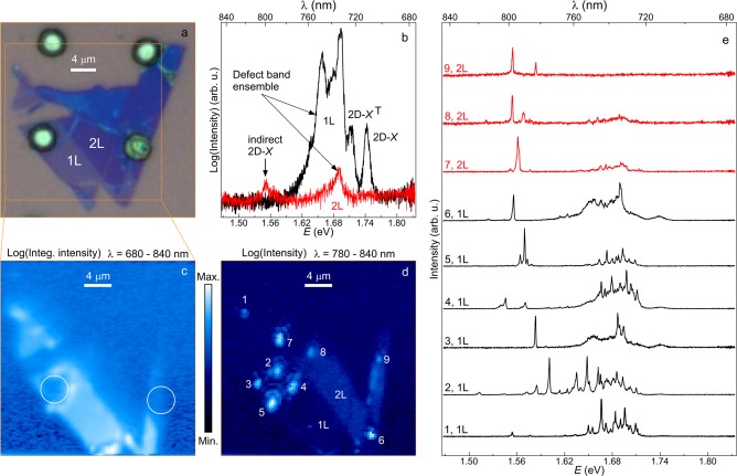
Using an all-dry viscoelastic stamping procedure,20 we transfer a mechanically exfoliated WSe2 flake (from bulk, nanoScience Instruments product NS00182) onto a Si substrate prepatterned with etched holes with a depth of 1 μm and a diameter of 4 μm. An optical micrograph of the sample is shown in Figure 1a; the gray region and four white disks represent the substrate and four etched holes, respectively, and the blue region corresponds to the WSe2 flake. The two lightest contrast regions of the flake are assigned as 1L and 2L regions. A portion of the 1L flake is successfully placed onto a prepatterned hole. Also observable in the contrast of the optical micrograph are a few wrinkles and small bumps in the flake. Using a confocal microscope (see Methods), nonresonant microphotoluminescence (μ-PL) spectra at an excitation power of 5 μW were obtained at the 1L and 2L positions of the corresponding labels in Figure 1a as shown by the black and red curves in Figure 1b, respectively. As expected, the 1L (2L) region shows a strong (weak) PL signal. The 1L spectrum shows two high energy peaks separated by ∼31 meV, corresponding to the quantum-well (2D) neutral exciton (2D-X) and a 2D charged exciton, or trion (2D-XT).21 The broadband emission centered at 1.68 eV for both 1L and 2L WSe2 is due to defect-bound excitons.19,21 Although the 1L band gap is direct, 2L WSe2 exhibits an indirect bandgap between the conduction band minimum at Σ and the valence band maximum at K in the first BZ.12 The weak emission peak centered at 1.55 eV in the 2L spectrum is due to this indirect 2D-X transition.
Figure 1.
(a) Optical micrograph of an exfoliated flake on top of a Si substrate with etched holes (1 μm deep, 4 μm diameter). (b) Typical PL emission spectra for 1L (black) and 2L (red) WSe2 from the smooth and unstrained locations of the flake. The ensemble emission due to defect-bound excitonic complexes can be seen in both 1L and 2L WSe2. (c–d) Color-coded spatial maps of PL with (c) integrated intensities in the spectral range of 680–840 nm and (d) intensities in the spectral range of 780–840 nm. (e) PL spectra corresponding to localized bright spots numbered in (d). The excitation power was 5 μW. The open square in (a) marks the region of spatial maps shown in (c) and (d). The two open circles in (c) mark the locations of the etched holes.
To investigate the spatial dependence of the PL spectrum on the flake, we scanned the entire region outlined by the yellow box in Figure 1a. Figure 1c shows the spatial map of the integrated intensities of the emission for 680 < λ < 840 nm, where the 1L region of the flake has intense PL and the remaining areas are dark. A one-to-one correspondence between Figure 1a and c can be seen. The two circles in Figure 1c mark the regions of holes underneath the flake. Note that the spatial map has been taken for a fixed focal plane, therefore the regions of the flake over the etched hole are significantly less bright due to alteration of the focal plane caused by buckling of the flake. When we generate a spatial map for 780 < λ < 840 nm, as shown in Figure 1d, then the indirect 2D-X emission from the 2L region of the flake is distinctively seen. Crucially, we also observe a few localized bright spots on the 1L flake around the edge of the etched hole and a few more isolated bright spots in both the 1L and 2L regions of the flake. These spots are numbered from 1 to 6 for 1L and 7–9 for 2L, and their corresponding spectra are shown in Figure 1e. The spectra from these bright spots are strikingly different from the typical emission spectra of 1L and 2L WSe2 (see Figure 1b). They show a comb-like emission in the region of the defect-band and very sharp emission lines at much lower energies. The comb-like emission has recently been reported,14−18 but the observation of such isolated, highly detuned peaks is unique. Tonndorf et al.18 have observed sharp emission lines on the shoulder of the ensemble defect band that are red-detuned by ∼60 meV from the ensemble mean. Here, we show single quantum emitters that are highly spectrally isolated, and in the extreme case (see spectrum 2, 1L in Figure 1e at location 2 in Figure 1d), their emission lines are red-detuned by ∼170 meV.
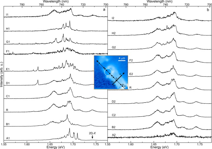
For further confirmation of the fact that the highly red-shifted 0D-X lines and the comb-like emission lines are only observed in the strong strain-gradient regions, we show the evolution of μ-PL spectra as the focus moves from the flat region of the flake (with local strain of < ± 0.05%) to the strong strain-gradient region of the flake (i.e., the region of the flake near the etched hole). This is summarized in Figure 2, which shows μ-PL spectra along two orthogonal lines passing through the reference point R on 1L WSe2 (see inset). The black points on these lines in the inset marks the selected locations where μ-PL spectra are chosen. Figure 2a shows the spectra along the long line which is passing through a tiny 1L flake at the bottom right corner followed by the 1L flat region and then the 1L region over the etched hole. The spectra along the short line, which covers only the 1L flat region, are shown in Figure 2b. First, the 0D-X band emission, which is fairly continuous in the flat part of the flake (point R), becomes more discrete, developing a comb-like appearance. Second, intense and sharp peaks emerge at energies both red- and blue-detuned from the center of the defect band (e.g., D1 and A1 in Figure 2a, respectively) due to tensile and compressive strain, respectively. On the other hand, almost no change in the 0D-X band emission is observed along the short line in Figure 2b, where the strain variation is minimal.
Figure 2.
Inset: Segment of Figure 1c superimposed with two orthogonal lines and with points A1 (A2), B1 (B2), ...I1 (I2) on the long (short) line. The arrows are guides to the eye for ascending order of these points and R refers to the intersection point of both lines. (a–b) PL spectra correspond to the points on (a) long and (b) short line marked in the inset.
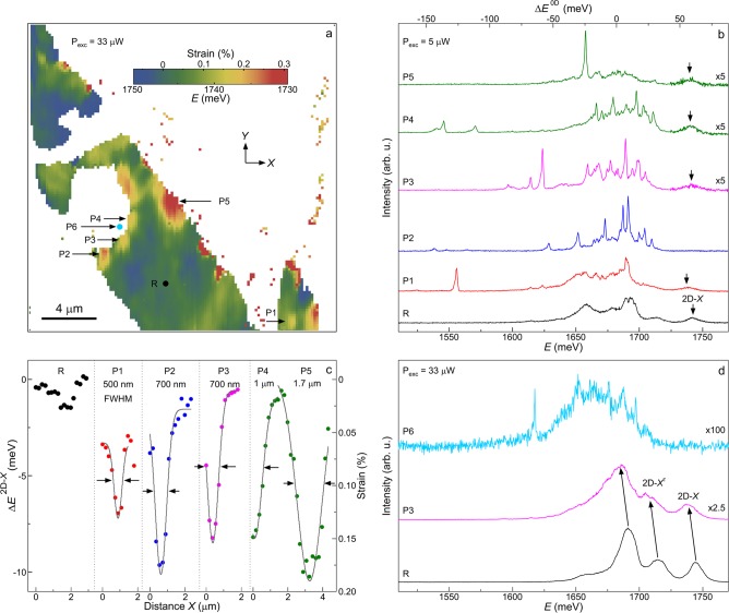
To better understand the origin of the isolated highly red-shifted emitters, we estimate the local strain in the 1L WSe2 by analyzing the peak energy of the 2D-X emission at an excitation power of 33 μW. The 2D-X peak energy map for the 1L region of the flake is shown in Figure 3a. We choose a reference point R on 1L WSe2 and estimate strain relative to this point. We use a calibration of −55 meV shift in the 2D-X peak energy for 1% uniaxial tensile strain (see Figure S5(b) of ref (12)). Note that strain estimation for 2L region of the flake and 1L region that spans the inner area of the patterned hole are not possible due to very weak 2D-X emissions (see the spectrum at P6 in Figure 3d). A strain variation of ∼ −0.05% (compressive) to 0.3% (tensile) across the 1L region of the flake is observed. The large portion of the 1L region of the flake that looks flat optically (see Figure 1a) shows a small strain variation (< ±0.05%). More importantly, a few highly localized energy minima are observed. We label five of these positions as P1 to P5. The region with the largest 2D-X red-shift, P5, is caused by a wrinkle propagating from the 2L region as seen in the optical micrograph (Figure 1a). P1 corresponds to a small bump which can be seen in the optical micrograph. Pockets P2–P4 are caused by bending of the flake around the edge of the etched hole. To characterize the spatial localization, we plot in Figure 3c the change in 2D-X peak energy (ΔE2D–X) for a horizontal line-cut through the center of the five highly strained regions. Notably, pockets P1–P3 show line widths (full width at half maximum, fwhm) approaching the diffraction limit of the confocal microscope, suggesting that actual strain variations are even more localized (<500 nm fwhm) than can be measured and are averaged out by the finite microscope resolution. Nevertheless, ΔE2D–X (estimated strain variation) as large as ∼ −10 meV (∼0.2%) is observed in the localized pockets.
Figure 3.
(a) Color-coded spatial map of the 2D-X peak energy for 1L WSe2, which includes a few localized energy minima. The energetic shift of the peak (ΔE2D–X) with respect to reference point R was used to estimate the strain. (b–c) (b) PL spectra and (c) horizontal cross-sectional ΔE2D–X/strain corresponding to reference point R and energy pockets P1 to P5 which correlates the effect of local strain gradients. (d) PL spectra corresponding to reference point R, P3, and P6. The excitation power for (a) and (d) were 33 μW and for (b) was 5 μW.
The μ-PL spectra corresponding to the local minima P1 to P5 and R are shown in Figure 3b. The spectra at the locations show highly red-shifted sharp emission lines together with the comb-like emission of the ensemble band. In the extreme cases (see spectrum 2, 1L in Figure 1e at location 2 in Figure 1d), a red-tuning of ∼170 meV is observed relative to the mean energy of the ensemble defect band in unstrained regions. Further strain-gradient correlations are found for all emitters in Figure 1d–e: four localized emitters occur at the edge of the patterned hole, the remaining occur at locations of unintentional strain. Conversely, the spectrum at R and elsewhere on the flat 1L region (see Figure 2b) shows only a broad band 0D-X ensemble. This direct correlation of localized strains and spatial and spectral emitter isolation leads to a robust conclusion that local strain variations disperse the energies of the individual defects in the 0D-X ensemble, resulting in comb-like emission within the nominal defect band and much larger red-tuning of a few defects at highly strained positions. Though we estimate a maximum strain of only ∼0.3%, we expect that larger strains exist at more highly localized spatial positions than we can measure because of the finite microscope resolution. An alternative explanation for the spectrally and spatially isolated emitters is localized contamination or chemical doping of the WSe2. To investigate the underlying cause of the structured broad ensemble we show three μ-PL spectra taken at locations R, P3, and P6 in Figure 3d. We observe that the ratio of 2D-X to 2D-XT intensities is maintained at positions R and at P3, the center of the broad defect ensemble moves linearly with the 2D-X and 2D-XT tuning, and the line width of the broad defect ensemble increases with increasing strain (see Figure S1 of Supporting Information for quantitative evidence). Note that the measurement of strain at location P6 was not possible because of the almost vanishing signal of 2D-X peak; however, a clear widening of the defect ensemble band can be seen in Figure 3d. These three observations strongly support the correlation of strain and emitter tuning rather than local substrate contamination or chemical doping.
The μ-PL emission spectrum at location 3 on 1L WSe2 flake (see Figure 1e) shows a sharp and spectrally isolated emitter at λ = 782.72 nm. High-resolution spectroscopy reveals a doublet split by Δ = 726 μeV with unequal intensities, as shown in Figure 4a. Each component of the doublet shows saturation and an excitation power (Pexc) dependent line width (see Figure 4b and c, respectively). The solid line in Figure 4b is a saturation curve fit for a two-level system using the relation I = Isat(Pexc/(Pexc + PN)), where PN = 2.78 μW is the normalization excitation power at which integrated intensity of the emission peaks becomes half of the saturation integrated intensity (Isat). It shows a linear power dependence at low Pexc and a clear saturation behavior at high Pexc. At the lowest Pexc, the minimum line widths measured are ∼60 μeV (fwhm). With increasing Pexc, increasing inhomogeneous broadening is observed. The inhomogeneous broadening is likely caused by fluctuating charges in the environment of the quantum emitter at a time scale faster than the experimental acquisition time. Also, modest spectral wandering is observed at longer time scales, as shown in the inset of Figure 4a. A naive expectation for a quantum emitter exposed at the surface is severe nonradiative recombination, inhomogeneous broadening, and photobleaching caused by nearby surface states. Surprisingly, the 0D-X states in WSe2, perhaps aided by the strong exciton binding energy, do not exhibit such deleterious features. Further, we find the amount of inhomogeneous broadening is directly linked to the nonresonant excitation power (Figure 4c), suggesting that quasi-resonant or strictly resonant excitation could lead to minimal electric field fluctuations and nearly transform limited line widths for 0D-X states.
Figure 4.
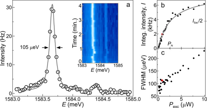
(a) High resolution PL spectrum of 0D-X from location 3 of Figure 1d. The experimental data is fit by two Lorentzian curves (gray line). The two peaks of the doublet are fine-structure-split 0D-X lines and the unequal peak intensities are due to anisotropic local strain. Inset: Spectral fluctuations of the doublet revealed using a color-coded time trace of the 0D-X lines. The time bin is 10 s. (b–c) Excitation power dependences of (b) integrated intensity and (c) line width of the low-energy 0D-X line. The gray line is the saturation curve fit. The red data points in (b) and (c) mark the representative positions for the spectrum shown in (a).
To investigate the nature of the doublet, we perform polarization-resolved and magneto-optical spectroscopy. Figure 5a shows a polarization-resolved intensity map of the doublet, revealing that the lines have unequal maximum intensities, are linearly polarized, and the angle between their polarization directions is 40°. We attribute the doublet to be the fine-structure of a neutral 0D-X. The symmetry breaking of the confinement potential leads to mixing of the two neutral excitonic states due to the electron–hole spin-exchange interaction, and therefore, the emission splits into two lines. The energetic separation between these two lines is called the fine-structure splitting (Δ).22,23 Here, we observe Δ = 726 μeV. Similar values of Δ were reported recently14−16 and the relatively large magnitude is likely due to the large long-range exchange interaction energy. Usually, two lines of the fine-structure split doublet have equal maximum intensities and are linearly polarized along orthogonal directions. The unequal intensities of the doublet lines and the nonorthogonality between their polarization directions of the emitter at location 3 can be ascribed to the presence of anisotropic strain.24 We have also performed polarization dependent PL for other emitters at locations with much less strain and find that the lines of the doublets show nearly equal maximum intensities and their polarization directions are nearly orthogonal to each other (see Figure 2S of Supporting Information).
Figure 5.
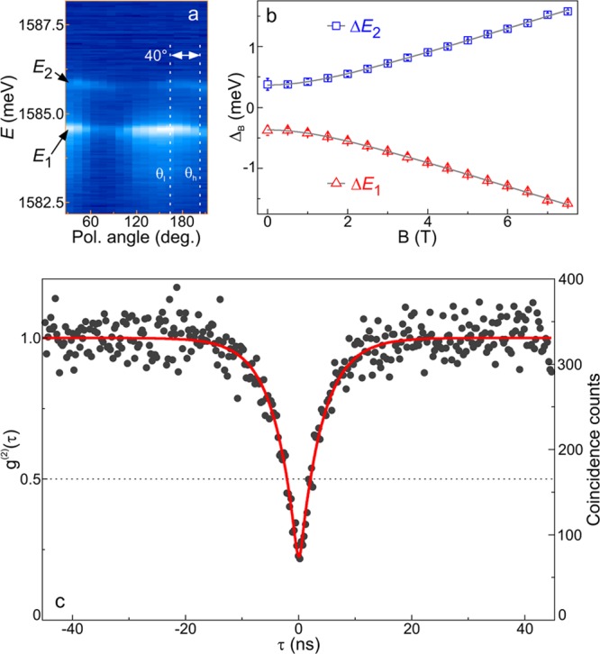
(a) Color-coded PL intensity as a function of polarization of the 0D-X lines at B = 2.5 T in Faraday geometry. The two dotted vertical lines show polarization direction of low-energy (θl) and high-energy (θh) 0D-X lines. A 40° angle between these directions also reflects the presence of anisotropic local strain. (b) Magnetic field dependence of the fine-structure split doublet. (c) Normalized second-order correlation function g(2)(τ) of the 0D-X lines under nonresonant cw excitation at P = 0.5PN. The fit (solid line) shows g(2)(0) = 0.17 and a lifetime of 4.14 ns.
The fine-structure split doublet’s behavior
in an external magnetic field (B) is illustrated
in Figure 5b. In the
Faraday geometry (direction of magnetic field perpendicular to the
flake plane), Δ is modified according to  , where μB is the Bohr magneton and g0D-X is exciton g-factor. The
clean fit of the data to ΔB affirm that both lines
of the doublet originate from a single neutral 0D-X; the fit reveals g0D-X = 7.16 ± 0.02. The large g0D-X is not understood but is in agreement with recent
reports.14−17 The large g0D-X inspires further investigations into the spin-valley degree of freedom
in the TMD quantum emitters. Additionally, B also
changes the central emission energy (EAvg.) of the doublet due to the diamagnetic shift,25 which is given by EAvg.(B) = EAvg.(0) + γ(B)2, where γ is the diamagnetic coefficient.
For this 0D-X, we measure γ = −3.9 ±
1.0 μeV/T2 (not shown). For a 3D confined system,
γ quantifies the combined contributions of confinement and Coulomb
interaction upon application of the magnetic field.25 The very small γ observed here demonstrates very
strong confinement of 0D-X.
Finally, we observe strong antibunched photon emission from this red-shifted emitter. Figure 5c presents the second-order correlation function g(2)(τ) under nonresonant cw excitation (P = 0.5 PN). The closed circles are measured data and the solid line is the fit using the relation g(2)(τ) = 1 – ρ2e–|τ|/T1, where T1 is the lifetime and SBR = ρ/(1 – ρ) is the signal-to-background ratio (SBR). We obtain g(2)(τ) = 0.17 ± 0.02 from the fit, unambiguously proving quantum emission. The fit yields T1 = 4.14 ± 0.15 ns and the estimated SBR here is ∼10.
In summary, we have achieved resolution-limited spatial localization of 0D-X with extremely low densities of ∼1 μm–2 within a 50 nm emission bandwidth (760 < λ < 810 nm) and tuning of the 0D-X emission energy over huge range (up to ≈170 meV). We directly correlate the 0D-X tuning and spatial and spectral isolation to microscopic pockets of large strain variation. These results demonstrate that strain engineering is a viable approach to obtain spatially and spectrally isolated quantum emitters in 2-D semiconductors. The passive exciton emission tuning observed with the 2D quantum emitters is significantly larger than the state-of-the-art for quantum emitters in bulk semiconductors.24,26−28 However, there is significantly more potential for strain engineering 0D-X states. First of all, massive strain gradients are possible in 2D materials7 and a number of approaches for both static or in situ tunable uniaxial and biaxial strain engineering can be considered.29 Second, the affect of strain on the electronic and optical properties of 0D-X states beyond their emission energy has yet to be investigated. For instance, in situ strain tuning can enable engineering of the carrier confinement potential,28 the permanent dipole moment, the fine-structure splitting,24,26,27 and the spin properties30 of localized exciton states. Notably, such quantum emitters could underpin a hybrid semiconductor-atomic interface.31,32 Finally, rather than suspending the flake over a large hole, by placing the flake over a nanostructured surface such as a periodic array of steps or holes, one can envisage periodic arrays of strained quantum emitters.
Methods
Experimental Setup
A confocal microscope with an objective lens with NA of 0.82, yielding a diffraction limited focus of ∼460 nm at λ = 750 nm, was used for μ-PL measurements with nonresonant CW excitation at λ = 532 nm. The microscope used dichroic mirrors at λ = 550 nm to separate the excitation and PL signals. The sample was placed on automated nanopositioners at T = 4 K in a closed-cycle cryostat with B = 0 to 9 T superconducting magnet. All spectra were acquired with a 0.5 m focal length spectrometer and nitrogen-cooled charge-coupled device with a spectral resolution of ∼40 μeV at λ = 750 nm for an 1800 L/mm grating. Polarization dependent PL was analyzed by combining a liquid-crystal variable retarder with a quarter wave plate and fixed linear polarizer. A fiber-based Hanbury-Brown and Twiss interferometer was used for second-order correlation measurements. Coincidence events from two Si avalanche photodiodes were recorded electronically on two synchronized input channels with a system timing jitter of ∼600 ps. Efficient spectral filtering (resolution ∼3 meV) was achieved using two angle-sensitive edge filters.
Acknowledgments
We thank A. Castellanos-Gomez for sharing his expertise on the dry transfer technique, R. Bernardo-Gavito and D. Granados for assistance assembling the microscope, J.M. Zajac for assistance with sample imaging, and A. Rastelli for data analysis software. This work was supported by a Royal Society University Research Fellowship, the EPSRC (grant numbers EP/I023186/1 EP/K015338/1, and EP/L015110/1) and an ERC Starting Grant (number 307392).
Supporting Information Available
The Supporting Information is available free of charge on the ACS Publications website at DOI: 10.1021/acs.nanolett.5b03312.
Quantitative analysis of strain-induced energetic shifts of excitonic peaks, fine-structure and polarization statistics of strained emitters and Figures S1–S2. (PDF)
Author Contributions
S.K. and A.K. contributed equally to this work.
The authors declare no competing financial interest.
Supplementary Material
References
- O’Brien J. L.; Furusawa A.; Vučković J. Nat. Photonics 2009, 3, 687–695 10.1038/nphoton.2009.229. [DOI] [Google Scholar]
- Santori C.; Fattal D.; Yamamoto Y.. Single-photon devices and applications; John Wiley & Sons: Hoboken, NJ, 2010. [Google Scholar]
- Lodahl P.; Mahmoodian S.; Stobbe S. Rev. Mod. Phys. 2015, 87, 347. 10.1103/RevModPhys.87.347. [DOI] [Google Scholar]
- Warburton R. J. Nat. Mater. 2013, 12, 483–493 10.1038/nmat3585. [DOI] [PubMed] [Google Scholar]
- Gao W. B.; Imamoglu A.; Bernien H.; Hanson R. Nat. Photonics 2015, 9, 363. 10.1038/nphoton.2015.58. [DOI] [Google Scholar]
- Xu X.; Yao W.; Xiao D.; Heinz T. F. Nat. Phys. 2014, 10, 343. 10.1038/nphys2942. [DOI] [Google Scholar]
- Bertolazzi S.; Brivio J.; Kis A. ACS Nano 2011, 5, 9703. 10.1021/nn203879f. [DOI] [PubMed] [Google Scholar]
- He K.; Poole C.; Mak K. F.; Shan J. Nano Lett. 2013, 13, 2931–2936 10.1021/nl4013166. [DOI] [PubMed] [Google Scholar]
- Conley H. J.; Wang B.; Ziegler J. I.; Haglund R. F. Jr; Pantelides S. T.; Bolotin K. I. Nano Lett. 2013, 13, 3626–3630 10.1021/nl4014748. [DOI] [PubMed] [Google Scholar]
- Castellanos-Gomez A.; Roldán R.; Cappelluti E.; Buscema M.; Guinea F.; van der Zant H. S.; Steele G. A. Nano Lett. 2013, 13, 5361–5366 10.1021/nl402875m. [DOI] [PubMed] [Google Scholar]
- Zhu C.; Wang G.; Liu B.; Marie X.; Qiao X.; Zhang X.; Wu X.; Fan H.; Tan P.; Amand T.; Urbaszek B. Phys. Rev. B: Condens. Matter Mater. Phys. 2013, 88, 121301. 10.1103/PhysRevB.88.121301. [DOI] [Google Scholar]
- Desai S. B.; Seol G.; Kang J. S.; Fang H.; Battaglia C.; Kapadia R.; Ager J. W.; Guo J.; Javey A. Nano Lett. 2014, 14, 4592. 10.1021/nl501638a. [DOI] [PubMed] [Google Scholar]
- Xia F.; Wang H.; Xiao D.; Dubey M.; Ramasubramaniam A. Nat. Photonics 2014, 8, 899–907 10.1038/nphoton.2014.271. [DOI] [Google Scholar]
- Srivastava A.; Sidler M.; Allain A. V.; Lembke D. S.; Kis A.; Imamoglu A. Nat. Nanotechnol. 2015, 10, 491. 10.1038/nnano.2015.60. [DOI] [PubMed] [Google Scholar]
- He Y.-M.; Clark G.; Schaibley J. R.; He Y.; Chen M.-C.; Wei Y.-J.; Ding X.; Zhang Q.; Yao W.; Xu X.; Lu C.-Y.; Pan J.-W. Nat. Nanotechnol. 2015, 10, 497. 10.1038/nnano.2015.75. [DOI] [PubMed] [Google Scholar]
- Koperski M.; Nogajewski K.; Arora A.; Marcus J.; Kossacki P.; Potemski M. Nat. Nanotechnol. 2015, 10, 503. 10.1038/nnano.2015.67. [DOI] [PubMed] [Google Scholar]
- Chakraborty C.; Kinnischtzke L.; Goodfellow K. M.; Beams R.; Vamivakas A. N. Nat. Nanotechnol. 2015, 10, 507. 10.1038/nnano.2015.79. [DOI] [PubMed] [Google Scholar]
- Tonndorf P.; Schmidt R.; Schneider R.; Kern J.; Buscema M.; Steele G. A.; Castellanos-Gomez A.; van der Zant H. S.; Michaelis de Vasconcellos S.; Bratschitsch R. Optica 2015, 2, 347–352 10.1364/OPTICA.2.000347. [DOI] [Google Scholar]
- Tongay S.; Suh J.; Ataca C.; Fan W.; Luce A.; Kang J. S.; Liu J.; Ko C.; Raghunathanan R.; Zhou J.; Ogletree F.; Li J.; Grossman J. C.; Wu J. Sci. Rep. 2013, 3, 2657. 10.1038/srep02657. [DOI] [PMC free article] [PubMed] [Google Scholar]
- Castellanos-Gomez A.; Buscema M.; Molenaar R.; Singh V.; Janssen L.; van der Zant H. S. J.; Steele G. A. 2D Mater. 2014, 1, 011002. 10.1088/2053-1583/1/1/011002. [DOI] [Google Scholar]
- Wang G.; Bouet L.; Lagarde D.; Vidal M.; Balocchi A.; Amand T.; Marie X.; Urbaszek B. Phys. Rev. B: Condens. Matter Mater. Phys. 2014, 90, 075413. 10.1103/PhysRevB.90.075413. [DOI] [PubMed] [Google Scholar]
- Gammon D.; Snow E. S.; Shanabrook B. V.; Katzer D. S.; Park D. Phys. Rev. Lett. 1996, 76, 3005. 10.1103/PhysRevLett.76.3005. [DOI] [PubMed] [Google Scholar]
- Bayer M.; Ortner G.; Stern O.; Kuther A.; Gorbunov A. A.; Forchel A.; Hawrylak P.; Fafard S.; Hinzer K.; Reinecke T. L.; Walck S. N.; Reithmaier J. P.; Klopf F.; Schäfer F. Phys. Rev. B: Condens. Matter Mater. Phys. 2002, 65, 195315. 10.1103/PhysRevB.65.195315. [DOI] [Google Scholar]
- Kumar S.; Zallo E.; Liao Y. H.; Lin P. Y.; Trotta R.; Atkinson P.; Plumhof J. D.; Ding F.; Gerardot B. D.; Cheng S. J.; Rastelli A.; Schmidt O. G. Phys. Rev. B: Condens. Matter Mater. Phys. 2014, 89, 115309. 10.1103/PhysRevB.89.115309. [DOI] [Google Scholar]
- Walck S. N.; Reinecke T. L. Phys. Rev. B: Condens. Matter Mater. Phys. 1998, 57, 9088. 10.1103/PhysRevB.57.9088. [DOI] [Google Scholar]
- Ding F.; Singh R.; Plumhof J. D.; Zander T.; Křápek V.; Chen Y. H.; Benyoucef M.; Zwiller V.; Dörr K.; Bester G.; Rastelli A.; Schmidt O. G. Phys. Rev. Lett. 2010, 104, 067405. 10.1103/PhysRevLett.104.067405. [DOI] [PubMed] [Google Scholar]
- Trotta R.; Zallo E.; Ortix C.; Atkinson P.; Plumhof J. D.; van den Brink J.; Rastelli A.; Schmidt O. G. Phys. Rev. Lett. 2012, 109, 147401. 10.1103/PhysRevLett.109.147401. [DOI] [PubMed] [Google Scholar]
- Kuklewicz C. E.; Malein R. N. E.; Petroff P. M.; Gerardot B. D. Nano Lett. 2012, 12, 3761–3765 10.1021/nl301621u. [DOI] [PubMed] [Google Scholar]
- Roldan R.; Castellanos-Gomez A.; Cappelluti E.; Guinea F.. Strain Engineering in Semiconducting Two-Dimensional Crystals. 2015, arXiv:1504.07926. arXiv.org e-Print archive. http://arxiv.org/abs/1504.07926 (accessed October 2015). [DOI] [PubMed] [Google Scholar]
- Huo Y. H.; et al. Nat. Phys. 2014, 10, 46. 10.1038/nphys2799. [DOI] [Google Scholar]
- Akopian N.; Wang L.; Rastelli A.; Schmidt O. G.; Zwiller V. Nat. Photonics 2011, 5, 230. 10.1038/nphoton.2011.16. [DOI] [Google Scholar]
- Kumar S.; Trotta R.; Zallo E.; Plumhof J. D.; Atkinson P.; Rastelli A.; Schmidt O. G. Appl. Phys. Lett. 2011, 99, 161118. 10.1063/1.3653804. [DOI] [Google Scholar]
Associated Data
This section collects any data citations, data availability statements, or supplementary materials included in this article.


