

Revealing the relaxation mechanisms of hidden states in transition metal dichalcogenides leads to control of metastability.
Keywords: Metastable states, charge density waves, electronic crystals, ultrafast memory devices, nonequilibrium relaxation
Abstract
Controllable switching between metastable macroscopic quantum states under nonequilibrium conditions induced either by light or with an external electric field is rapidly becoming of great fundamental interest. We investigate the relaxation properties of a “hidden” (H) charge density wave (CDW) state in thin single crystals of the layered dichalcogenide 1T-TaS2, which can be reached by either a single 35-fs optical laser pulse or an ~30-ps electrical pulse. From measurements of the temperature dependence of the resistivity under different excitation conditions, we find that the metallic H state relaxes to the insulating Mott ground state through a sequence of intermediate metastable states via discrete jumps over a “Devil’s staircase.” In between the discrete steps, an underlying glassy relaxation process is observed, which arises because of reciprocal-space commensurability frustration between the CDW and the underlying lattice. We show that the metastable state relaxation rate may be externally stabilized by substrate strain, thus opening the way to the design of nonvolatile ultrafast high-temperature memory devices based on switching between CDW states with large intrinsic differences in electrical resistance.
INTRODUCTION
Macroscopic quantum states in systems such as superconductors and charge density waves (CDWs) have recently been shown to display nonequilibrium switching phenomena, arising from rapid transitions between the many-body ground state and a long-living metastable state (1–4). In constricted superconducting Bi2Sr2CaCu2O8+δ bridges (5) and Zn nanowires (3), current-driven switching occurs between a metastable dissipative inhomogeneous phase slip state and the homogeneous superconducting ground state. In related systems displaying structural or Mott transitions, laser photoexcitation may temporarily cause metastable ordering (6), but the system typically reverts back to the ground state within 10−9 to 10−3 s (6–12). In the dichalcogenide 1T-TaS2 CDW system, switching to a hidden (H) state is achieved either with an optical laser pulse (1) or by an electrical pulse (4). The remarkably fast switching recently demonstrated (by 35-fs optical and 30-ps electrical pulses, respectively), unprecedented stability, and large resistivity changes accompanying the switching make this system uniquely attractive for potential nonvolatile memory devices. Compared with other candidates for next-generation computer memories, such as memristors (13) and resistive phase change memory devices (14, 15), such potential CDW devices are remarkably fast (16, 17). The switching was thought to arise as a result of a nonequilibrium transition from a commensurate (C) low-temperature ground state to an H metallic state with different charge order, which does not normally exist under the experimental conditions in hand (1).
Under equilibrium conditions, complex charge-ordered states in 1T-TaS2 arise as a consequence of the competition of Coulomb repulsion, lattice strain, and Fermi surface nesting, which transforms the material from a simple metal at high temperatures to an incommensurate (IC) CDW at 550 K. Frustration arising from the incommensurability of this state with the underlying lattice causes the IC CDW to transform into a nearly commensurate (NC) structure at ~350 K in which patches of commensurately ordered hexagram-shaped polarons are periodically separated by domain walls (18). Each polaron, as determined by electron diffraction (19), consists of a single electron localized on a Ta atom, with 12 surrounding Ta atoms slightly displaced toward the center (20, 21), as shown in Fig. 1. On cooling from room temperature, the domain walls disappear in a first-order transition near 180 K, and the material becomes a gapped, commensurately ordered Mott insulator as schematically shown in Fig. 1. The quantum nature of CDWs has been controversial (22), and for a long time, there was a prevailing view that most phenomena in CDW systems in general may be classically described. However, more recent Aharonov-Bohm interference experiments in macroscopic rings of NbSe3 with correlation lengths of over 100 μm at temperatures as high as 79 K seemingly defy a classical description (23). Furthermore, unusual spontaneous switching similar as in superconductors (3) has been reported in CDWs, which cannot be described in terms of the usual narrow-band noise accompanying the sliding motion of the CDW or any other known related phenomena (2, 4).
Fig. 1. Schematic description of the experiment and basic switching behavior.
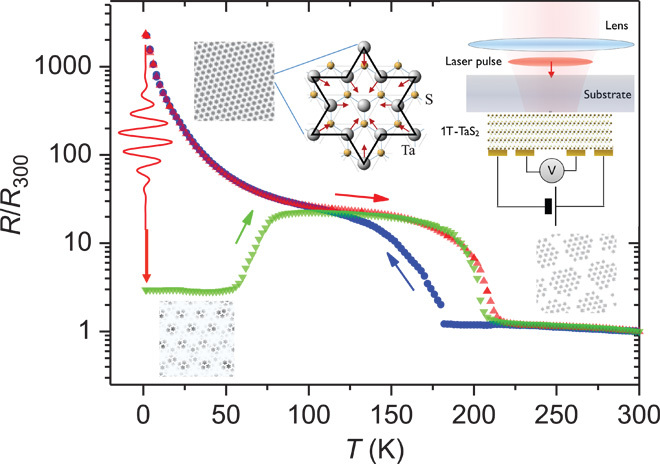
The unperturbed resistance is shown in the C state on cooling (blue data points) and on heating (red data points). The green curve shows the resistance in the H state after switching by a single 35-fs optical pulse above threshold. A schematic representation of the ordered phases C and NC is shown, with an indicated tentative ordering for the H state. The inset shows a schematic description of the experimental setup.
An important property of the metastable CDW state in 1T-TaS2 is its extremely long lifetime. Stojchevska et al. (1) proposed that the remarkable stability of the system arises from a topological protection mechanism where topological defects need to be introduced to reach the homotopically distinct ground state from the H state. Microscopically, this requires a conversion of particles from band states to (gapped) localized states, which is energetically costly. Whereas in crystals it is the ordering of atoms that causes topological defects, here it is the topology of the electronic order that is relevant. However, the relaxation dynamics of the H state may be expected to show behavior reminiscent of dislocation dynamics in crystals or a transition between C and IC orders (24), where many different topologically distinct intermediate states may be present in the relaxation pathway. So far, there are no experimental data on this transformation of the H state in 1T-TaS2. Here, we report on the relaxation dynamics through measurements of the electrical resistivity of the H state of 1T-TaS2. The observations lead to an understanding of the relaxation processes that may open the way to practical design of new ultrafast data storage devices operating above room temperature. Following the recent indications showing that strain has an effect on the temperature stability of the H state (25), we also show how the relaxation dynamics can be effectively controlled by substrate strain.
In Fig. 1, we show the temperature dependence of the resistance R in a typical 1T-TaS2 crystal and the effect of optical switching from the C to the H state. The sample is first cooled to 1.5 K, then a 35-fs laser pulse is applied through the substrate, with a fluence above switching threshold (1), and the resistance is measured on slow heating. As the H state thaws, the resistance reverts back to the C state value at a temperature TH ~57 K, which strongly depends on the heating rate (presently ~1 K/min). The resistance of the H state after switching shows reproducible saturation (Fig. 1).
To measure the temperature dependence of the relaxation of the H state, we switch the state with the laser pulse at a fixed temperature, and then measure R as a function of time. Figure 2A shows a plot of the relaxation at different temperatures for a sample on a sapphire substrate, in the range from 30 to 75 K. The data show that the τH decreases rapidly with increasing T. Above ~70 K, τH becomes comparable to the measurement time for each point, whereas below 30 K, it becomes too long to practically measure. The relaxation shows small jumps at certain values of resistance (Fig. 2) that cannot be attributed to noise or mechanical relaxation. The positions and magnitude of the jumps are sample-dependent.
Fig. 2.
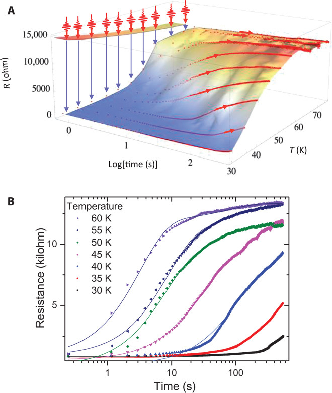
(A) Relaxation of the resistance R as a function of temperature after switching from the C to the H state. Before each measurement, the sample is heated above Tc2 and then cooled to the indicated temperature. After exposure to a single 35-fs laser pulse, the resistance is continuously measured as a function of time. (B) Fits to R(t) at different T using a stretched exponential function.
In Fig. 2B, we show fits to the relaxation curves (ignoring the jumps) using a stretched exponential relaxation (SER) function R = R0[1 − exp(−(t/τH)β)], commonly used in “glassy” relaxation processes (26). Here, τH and β are fitting parameters.
The relaxation dynamics after switching by current pulses is qualitatively similar to the optical switching, except that here the jumps in the relaxation are slightly more pronounced. We attribute this to the fact that these devices are smaller, with a smaller distance between contacts (1 to 8 μm compared to ~50 μm in optical devices), so the electrical current switching devices have better-defined boundary conditions imposed by the contacts. In Fig. 3A, we show the relaxation dynamics after switching with a 10-μs current pulse at different temperatures, whereas in Fig. 3B, we show the stretched exponential fits to the data. Calculating the difference between the fitted stretched exponential and the raw data in Fig. 3B clearly exposes a set of aperiodic oscillations superimposed on the SER. In Fig. 4, we show a summary of the T dependence of τH in an Arrhenius plot combining the optical and electrical switching data. Large variations in the T dependence of τH are observed, depending on both the excitation method and the sample substrate. Comparing sapphire and quartz substrates, we observe quite significant differences in the relaxation time, τH being much longer on sapphire than on quartz at any given temperature. Extracting an activation energy EA from fitting an Arrhenius law 1/τH = exp(−EA/kBT) (where kB is Boltzmann constant) to the temperature dependence of τH in Fig. 4, we obtain good fits, with values of EA between 280 and 2300 K, depending on the sample and the substrate. Surprisingly, the exponent β appears to be strongly T-dependent, rapidly decreasing with increasing T as shown in Fig. 4B.
Fig. 3. Relaxation of the resistance after switching to the H state with electrical pulses.
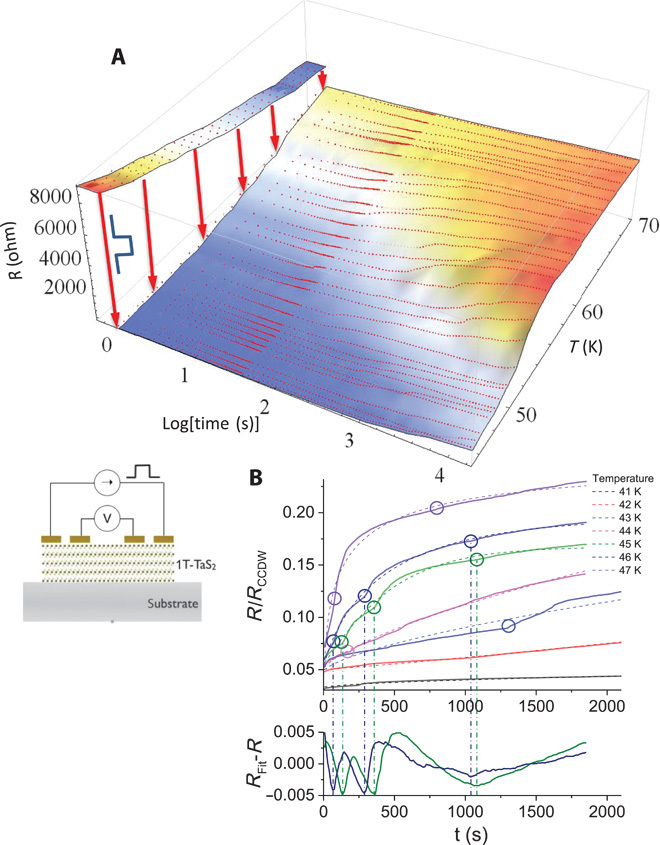
(A) R(t) at different temperatures after switching at t = 0. The inset shows a schematic diagram of the circuit. Before each measurement, the sample is heated above Tc2 and then cooled to the indicated temperature. After exposure to a 5-μs electrical pulse, the resistance is measured as a function of time. (B) Relaxation at a few selected temperatures with stretched exponential fits. The residual resistance RFit − R obtained after subtracting the stretched exponential fit from the raw data shows distinct aperiodic oscillations with time.
Fig. 4. Relaxation rate 1/τH and the exponent as a function of 1/T.
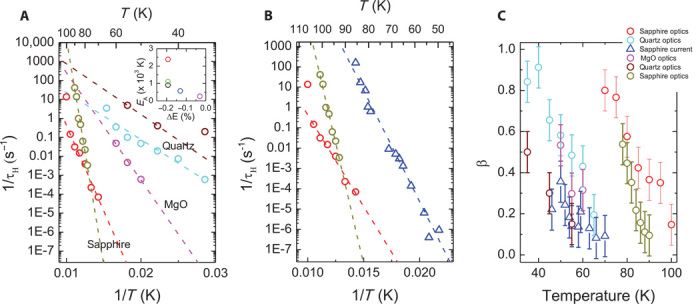
(A) A comparison of substrates with different tensile strain on a number of samples, also showing the sample-to-sample variation. The strain imposed by the sapphire, MgO, and quartz substrates at 50 K is 0.19, 0.13, and 0.03%, respectively (25). (B) A comparison for current and optical switching methods on sapphire. (C) Stretched exponent shows similar trend with T, irrespective of substrate or method of excitation. The legend shown in (C) applies to all three panels. The raw relaxation data for MgO and quartz substrates are shown in fig. S2A.
RELAXATION FROM AN IC TO A C STRUCTURE
The process of relaxation from a metal (H) to an insulator (C) state in 1T-TaS2 is highly nontrivial and involves microscopic processes of carrier conversion from band states to localized polaronic states, mesoscopic ordering of polarons due to Coulomb interactions, and eventually macroscopic relaxation of a long-range frustrated IC structure.
The transformation from the H to the C state may be thought to be qualitatively similar to a NC→C transition in 1T-TaS2. However, the resistivity of the H state differs from that of the supercooled NC state (see the Supplementary Materials), so the H state was proposed to have a slightly different charge order than the NC state (1). Moreover, our experiments show that relaxation between the supercooled NC state and the C state is unmeasurably short on the time scale of the resistance measurement (see the Supplementary Materials) and is thus quite different from the slow H state relaxation. Comparing our data with the relaxation of deeply quenched samples in the high-temperature IC state of 1T-TaS2 (27), we find that in the IC state, the fits of the time dynamics with an SER function give β = 1.5 ± 0.1 and an activation energy of ~4600 K, where both are T-independent. In other prototypical quasi–one-dimensional (1D) systems like blue bronze, the dynamics also shows SER but with β = 0.65 to 0.7 (28), which is again T-independent. In contrast, the relaxation of the H state resistance shown in Figs. 2 and 3 proceeds in a more complex way. In particular, the SER β exponent rapidly decreases with increasing temperature (Fig. 4B), different from what is usually observed, where it either is constant or occasionally even increases with T (26). Moreover, τH has a much wider range of activation energies from 280 to 2300 K (Fig. 4A), which is also different from the behavior observed before. The presence of SER, together with stability of the H phase below 40 K, indicates that we are dealing with a microscopic glassy relaxation process (26, 29). The most common cause for the glassiness is an associated distribution of energy scales and relaxation times resulting from the pinning of the CDW by impurities and other defects of the underlying lattice. In the next section, we shall show how the microscopic polaron dynamics associated with the relaxation process may also lead to SER.
On the other hand, the jumps are expected to result from abrupt adaptation(s) of an IC superstructure to the underlying lattice on a larger scale, where entire domains simultaneously readjust. Thus, a variety of phenomena (24) are expected, from a smoother version of a rising periodic superstructure of discommensurations (the phase solitons) to a discrete sequence of jumps over a “Devil’s staircase” with complicated intermediate metastable structures with different degrees of discommensurability (24, 29, 30). We may describe the problem in terms of the Frenkel-Kontorova (FK) model (30) by the Hamiltonian:
| (1) |
where xn are the positions of the n-th density wave maxima and a is the period of the underlying lattice. Its solutions form a Cantor function, where the relaxation of the system in time proceeds through a series of states with discrete steps with different wave numbers q (the Devil’s staircase). Extending the FK model to the continuum limit (31), Eq. 1 reduces to the sine-Gordon equation with solitonic solutions (the domain walls). In the continuum limit, the discrete steps are smoothed out (as described in more detail in the Supplementary Materials). The present system displays both discrete jumps and smoothed-out intermediate structures, so neither model is entirely applicable. In the absence of detailed structural information, we are forced to stay here with a qualitative picture. Initially, when incommensurability is large, the relaxation proceeds in large steps of displacement, eliminating domain walls in the process. As the mismatch decreases, the jumps become smaller, approaching a more continuous relaxation curve. At low T, the relaxation is arrested by pinning at crystal imperfections and crystal boundaries.
THE MICROSCOPIC PICTURE: FROM METAL TO INSULATOR
Although the overall curve R(t) is determined by large-scale topological rearrangements of an IC CDW, the steps in between may be viewed as a microscopic nucleation process, consistent with the general microscopic picture in this material. Consider an H state composed of patches of polarons separated by polaron-free domain walls (see Fig. 5 for a schematic representation and corresponding energy level diagrams). In the C state, these are filled, so the H→C relaxation primarily involves the thermally activated self-trapping of electrons from delocalized band states into polarons, gradually filling the domain walls in between the ordered polaron patches. Each time an electron becomes localized, a state is converted from the delocalized metallic band to the polaronic one, eventually completely depleting the metallic band (Fig. 5). During this process, the spatial polaron distribution is forced to reorganize by the Coulomb interaction, gradually changing the domain wall periodicity in steps of different size, which we can understand in terms of the physics of the FK model. The maximum activation energy EA ≈ 2300 K approaches the energy scale for activated hopping from itinerant states at the Fermi level to the unoccupied states in the UHB. However, because a doubly occupied UHB is unstable, it very rapidly decays, forming a new self-trapped polaron and one new Mott-Hubbard state in the process (Fig. 5). One may view this second step as a process in which the doubly occupied polaron releases its Coulomb energy by a “mitosis” into two singly occupied polarons, which forms an elementary relaxation step toward the C phase.
Fig. 5. Schematic diagram of the elementary relaxation process.
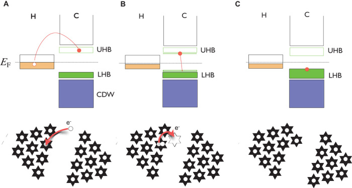
(A) Thermal excitation of an electron (e−) from itinerant band states at the Fermi level in the H state into the upper Hubbard band (UHB). LHB, lower Hubbard band; EF, Fermi energy. (B) Relaxation of one of the electrons. (C) Creation of a new polaron in the domain wall.
The gradual filling in of domain walls by polarons can be discussed in terms of a two-stage picture of phase transformations (32) by which an initial nucleation of polarons into patches is followed by an Ostwald ripening (OR) process occurring on longer time scales, where larger polaron patches grow at the expense of the evaporation of smaller ones (33). If we assume that the H state is similar to the NC state, in the H state, there is relatively little room for new patches within existing domain walls, so the OR process is expected to be dominant in which polarons created within the domain walls migrate toward energetically favorable positions at the edges of existing polaron patches. In the Supplementary Materials, we show that such a two-stage relaxation process, with an initial double-exponential time dependence followed by a power-law relaxation at long times, can be fit to the data. Unfortunately, even without taking into account the propensity to long-range ordering imposed by the Coulomb interaction competing with strain, the model has seven fitting parameters, which somewhat limit its value.
A simpler model, but still within the OR picture, can be devised by considering just the growth of polaron clusters at the expense of single polarons in the domain walls. This process involves many different polaron configurations (such as the one as shown in Fig. 5), which can have a range of different energy states and whence a range of relaxation times. This immediately leads to an SER model used in the fits to our data. In the Supplementary Materials, we show that the quality of the fit of such a model is nearly as good as the two-component model described in the previous paragraph, but with only two adjustable parameters. Thus, the SER model can be regarded as a useful tool for a phenomenological description of the relaxation, which is consistent with the microscopic picture. Ultimately, lattice imperfections, impurities, substrate strain, and other external parameters also have an effect on the nucleation process, which gives rise to a large spread of time and energy scales in the relaxation process.
THE EFFECT OF STRAIN AND BOUNDARY CONDITIONS
The very strong dependence of the relaxation dynamics on the in-plane strain shows the possibility of effectively controlling the relaxation of the H state. The tensile strain Δϵ imposed by the differential contraction of the substrate and the sample is quite small (from −0.19% for sapphire to −0.03% for quartz), but the effect on the relaxation properties is quite large, which implies that the effect of strain is not a microscopic effect on the level of the unit cell. As the lattice expands, the electron density n changes. In the present case of a threefold quasi-1D CDW, this gives rise to a change of q in the H state beyond the change resulting from the expansion of the underlying lattice. So, the thermal expansion coefficients of the lattice and the CDW are not the same, and strain leads to a change of commensurability. Furthermore, the contacts at the edges of the sample provide boundary conditions at which the CDW is pinned. A change of dimensions induced by strain requires a rearrangement of the CDW, which proceeds in a quantized fashion, leading to resistance steps as previously shown in K0.3MoO3 (34), whereas the possible effect of strain on the commensurability was discussed in NbSe3 (35). If we assume that the H state is qualitatively similar to the NC state with a distance of ~8 nm between domain walls, a strain of 0.2% over a distance of 1 to 10 μm between contacts introduces about one to two extra domain walls in each in-plane direction. The relaxation from the H to the C state involves the removal of domain walls, accompanying the conversion from itinerant to localized states. A compressive strain also acts to remove domain walls, thus effectively lowering the activation energy EA. On the other hand, a tensile strain has the opposite effect of stabilizing the domain wall structure, increasing EA and TH (25), consistent with the data shown in the inset of Fig. 4A.
The fundamental relaxation mechanisms of the metastable H state in 1T-TaS2 revealed by the present experiments indicate that it is possible to externally control the metastable state relaxation parameters. This is of crucial importance for increasing the stability of the H state and rapid thermal erasure of the metastable state in ultrafast nonvolatile memory devices. The fact that different samples display significant differences in EA implies that additional external parameters, such as nanopatterned structural features, local defects, and doped impurities, which introduce pinning, provide a means to control the stability of the H state. This leads the way to new artificial structures as the next step toward devices based on manipulation of CDW states and a new generation of ultrafast computer memories. In addition to record switching speeds [30 ps electrical (4), recently confirmed by Hollander et al. (36); and 35 fs optical (1)] and low dissipation (4), the data retention stability can be controlled. Electrical switching allows parallel address devices to be made using existing crossbar architectures. The possibility of low-temperature operation is an advantage for ultrafast operation in mainframe machines where heat dissipation limits computer speed.
METHODS
For both types of measurements, single crystals were deposited on sapphire, MgO, or quartz substrates by exfoliating with sticky tape and directly redepositing the exfoliated flakes onto the substrate. The substrate materials exert different tensile strain on the 1T-TaS2 crystals upon cooling because of the mismatch of the lattice expansion between the sample and the substrates, the sapphire exerting a strain on the 1T-TaS2 of ϵ = −0.19%, whereas the values for MgO and quartz are −0.13 and −0.03%, respectively, at 50 K (25). The thicknesses of the films deposited in this investigation are between 20 and 100 nm. However, films thinner than ~20 nm showed switching to the NC state (see the Supplementary Materials), so all the presented data are on samples that are 100 ± 15 nm thick. The crystal c axis of the samples is perpendicular to the plane of the substrate. Typical lateral dimensions were 100 mm, allowing four gold contacts to be deposited on the samples using laser direct photolithography with an LPKF ProtoLaser LDI laser writer. The contacts were made with a 5-nm Au/Pd intermediate layer before sputtering of 100 ± 20–nm–thick gold electrodes. For electrical switching, typical intercontact distances are between 1 and 8 μm on crystals typically 4 to 6 μm wide. The optical switching was performed by illuminating the device through the substrate with 35-fs pulses from 1 kHz–amplified Ti-sapphire laser to avoid shadows from the contacts as shown in the inset of Fig. 1. The intercontact distance was typically larger (~50 μm), whereas the beam diameter was ~100 μm. Our scanning tunneling microscopy (STM) characterization studies show that impurities are present but cannot be easily correlated with the switching characteristics. The estimated impurity concentration (from our STM images) is <1 per 30 × 30–nm2 area, so the impurity concentration corresponds to <0.1% polaron sites. The presence of a strong resistance upturn at low temperatures (note log scale in Fig. 1) confirms that the number of impurities is small (37).
The optical penetration depth at 800 nm is 22 nm, so the laser fluence was adjusted to achieve saturation of the resistance in the H state, typically Φ ~4 mJ/cm2. Electrical switching was performed with electrical pulses using a Keithley 6221 Current Source and Keithley 2182A Nanovoltmeter for “write” (W) pulse durations τW = 5 ms (4). The resistivity is read with low currents typically Iread = 0.1 μA in pulsed mode. The measurement time for each data point is 50 μs, and the time between measurements is 0.1 to 1 s. This limits the shortest lifetime that could be measured. The circuit is schematically shown in the inset of Fig. 3. For intermediate pulse durations 20 ns < τW < 5000 ns, we used a Stanford DG535 pulse generator and a Texas Instruments THS4211EVM amplifier. The switching was previously shown to be qualitatively the same for 30-ps pulses (4). The resistivity of the switched state is read with low currents typically Iread = 0.1 μA in pulsed mode. The “read” operation was observed to have no measurable effect on the state lifetime.
Funding
This work was supported by the Slovenian Research Agency, European restructuring funds (CENN Nanocenter), and European Research Council advanced grant TRAJECTORY. Author contributions: I.V. performed experiments, analyzed the data, and prepared figures. J.G. and I.A.M. performed experiments. D.S. prepared the samples and made lithography. P.S. synthesized the crystals. E.G. checked the quality of the crystals by x-ray diffraction. S.B. developed the modeling. T.M. assisted with experiments. D.M. analyzed the data, developed the model, and prepared the manuscript. Competing interests: The authors declare that they have no competing interests.
SUPPLEMENTARY MATERIALS
Supplementary material for this article is available at http://advances.sciencemag.org/cgi/content/full/1/6/e1500168/DC1
Fig. S1. Temperature dependence of 20-nm-thick sample for different cooling-warming rates.
Fig. S2. Temperature and fluence dependence of relaxation of the H state.
Fig. S3. Schematic representation of the IC and H state relaxation in one dimension.
Fig. S4. The numerous minima of the energy given by Eq. 1 form different metastable states of the system.
Fig. S5. The phase shift and CDW density for a particular configuration of domain walls.
Fig. S6. A comparison of fits with three different models to the data at 45 K described in the text.
REFERENCES AND NOTES
- 1.Stojchevska L., Vaskivskyi I., Mertelj T., Kusar P., Svetin D., Brazovskii S., Mihailovic D., Ultrafast switching to a stable hidden quantum state in an electronic crystal. Science 344, 177–180 (2014). [DOI] [PubMed] [Google Scholar]
- 2.Tsubota M., Inagaki K., Matsuura T. and Tanda S., Aharonov-Bohm effect in charge-density wave loops with inherent temporal current switching. Europhys. Lett. 97, 57011 (2012). [Google Scholar]
- 3.Chen Y., Lin Y.-H., Snyder S. D., Goldman A. M., Kamenev A., Dissipative superconducting state of non-equilibrium nanowires. Nat. Phys. 10, 567–571 (2014). [Google Scholar]
- 4.Vaskivskyi I., Mihailovic I. A., Brazovskii S., Gospodaric J., Mertelj T., Svetin D., Sutar P., Mihailovic D., Fast non-thermal switching between macroscopic charge-ordered quantum states induced by charge injection. arXiv 1409.3794 (2014). [Google Scholar]
- 5.Zybtsev S. G., Pokrovskii V. Y., Gorlova I. G., Latyshev Y. I., Timofeev V. N., Instabilities in the current-voltage characteristics of submicron BSCCO bridges. J. Phys.: Conf. Ser. 43, 643–646 (2006). [Google Scholar]
- 6.K. Nasu, Photoinduced Phase Transitions (World Scientific Publishing Co. Inc., Hackensack, NJ, 2004). [Google Scholar]
- 7.Koshihara S., Tokura Y., Mitani T., Saito G., Koda T., Photoinduced valence instability in the organic molecular compound tetrathiafulvalene-p-chloranil (TTF-CA). Phys. Rev. B Condens. Matter 42, 6853–6856 (1990). [DOI] [PubMed] [Google Scholar]
- 8.Koshihara S., Tokura Y., Takeda K., Koda T., Dynamics of a photoinduced phase transition in polydiacetylene crystals. Phys. Rev. B Condens. Matter 52, 6265–6272 (1995). [DOI] [PubMed] [Google Scholar]
- 9.Okamoto H., Ishige Y., Tanaka S., Kishida H., Iwai S., Tokura Y., Photoinduced phase transition in tetrathiafulvalene-p-chloranil observed in femtosecond reflection spectroscopy. Phys. Rev. B 70, 165202 (2004). [Google Scholar]
- 10.Cavalleri A., Tóth C., Siders C. W., Squier J. A., Ráksi F., Forget P., Kieffer J. C., Femtosecond structural dynamics in VO2 during an ultrafast solid-solid phase transition. Phys. Rev. Lett. 87, 237401 (2001). [DOI] [PubMed] [Google Scholar]
- 11.Takubo K., Son J. Y., Mizokawa T., Takubo N., Miyano K., Observation of photoinduced phase transition in phase-separated Pr0.55(Ca1−ySry)0.45MnO3 thin films via x-ray photoemission spectroscopy. Phys. Rev. B 75, 052408 (2007). [Google Scholar]
- 12.Yu G., Lee C. H., Heeger A. J., Herron N., McCarron E. M., Cong L., Spalding G. C., Nordman C. A., Goldman A. M., Phase separation of photogenerated carriers and photoinduced superconductivity in high-Tc materials. Phys. Rev. B 45, 4964–4977 (1992). [DOI] [PubMed] [Google Scholar]
- 13.Yang J., Pickett M., Li X., Ohlberg D., Stewart D. R., Williams R. S., Memristive switching mechanism for metal/oxide/metal nanodevices. Nat. Nanotechnol. 3, 429–433 (2008). [DOI] [PubMed] [Google Scholar]
- 14.Wong H.-S. P., Raoux S., Kim S., Liang J., Reifenberg J. P., Rajendran B., Asheghi M., Goodson K. E., Phase change memory. Proc. IEEE 98, 2201–2227 (2010). [Google Scholar]
- 15.Loke D., Lee T. H., Wang W. J., Shi L. P., Zhao R., Yeo Y. C., Chong T. C., Elliott S. R., Breaking the speed limits of phase-change memory. Science 336, 1566–1569 (2012). [DOI] [PubMed] [Google Scholar]
- 16.Kent A. D., Worledge D. C., A new spin on magnetic memories. Nat. Nanotechnol. 10, 187–191 (2015). [DOI] [PubMed] [Google Scholar]
- 17.Wong H. S. P., Salahuddin S., Memory leads the way to better computing. Nat. Nanotechnol. 10, 191–194 (2015). [DOI] [PubMed] [Google Scholar]
- 18.Nakanishi K., Shiba H., Domain-like incommensurate charge-density-wave states and the first-order incommensurate-commensurate transitions in layered tantalum dichalcogenides. I. 1T-polytype. J. Phys. Soc. Jpn. 43, 1839–1847 (1977). [Google Scholar]
- 19.Wilson J., Di Salvo F., Mahajan S., Charge-density waves and superlattices in the metallic layered transition metal dichalcogenides. Adv. Phys. 24, 117–201 (1975). [Google Scholar]
- 20.Thomson R., Burk B., Zettl A., Clarke J., Scanning tunneling microscopy of the charge-density-wave structure in 1T-TaS2. Phys. Rev. B Condens. Matter 49, 16899–16916 (1994). [DOI] [PubMed] [Google Scholar]
- 21.Burk B., Thomson R., Clarke J., Zettl A., Surface and bulk charge density wave structure in 1T-TaS2. Science 257, 362–364 (1992). [DOI] [PubMed] [Google Scholar]
- 22.Bardeen J., Classical versus quantum models of charge-density-wave depinning in quasi-one-dimensional metals. Phys. Rev. B Condens. Matter 39, 3528–3532 (1989). [DOI] [PubMed] [Google Scholar]
- 23.Miller J. Jr, Wijesinghe A., Tang Z., Guloy A., Coherent quantum transport of charge density waves. Phys. Rev. B 87, 115127 (2013). [Google Scholar]
- 24.Bak P., Commensurate phases, incommensurate phases and the devil’s staircase. Rep. Prog. Phys. 45, 587–629 (1982). [Google Scholar]
- 25.Svetin D., Vaskiskyi I., Sutar P., Goreshnik E., Gospodaric J., Mertelj T., Mihailovic D., Transitions between photoinduced macroscopic quantum states in 1T-TaS2 controlled by substrate strain. Appl. Phys. Express 7, 103201 (2014). [Google Scholar]
- 26.Phillips J. C., Stretched exponential relaxation in molecular and electronic glasses. Rep. Prog. Phys. 59, 1133–1207 (1996). [Google Scholar]
- 27.Su J.-D., Sandy A. R., Mohanty J., Shpyrko O. G., Sutton M., Collective pinning dynamics of charge-density waves in 1T-TaS2. Phys. Rev. B 86, 205105 (2012). [Google Scholar]
- 28.Kriza G., Mihály G., Stretched-exponential dielectric relaxation in a charge-density-wave system. Phys. Rev. Lett. 56, 2529–2532 (1986). [DOI] [PubMed] [Google Scholar]
- 29.Brazovskii S., Nattermann T., Pinning and sliding of driven elastic systems: From domain walls to charge density waves. Adv. Phys. 53, 177–252 (2004). [Google Scholar]
- 30.Kontorova T., Frenkel J., On the theory of plastic deformation and twinning, I.. Zh. Eksp. Teor. Fiz. 8, 1 (1938). [Google Scholar]
- 31.Aubry S., Gosso J.-P., Abramovici G., Raimbault J.-L., Quemerais P., Effective discommensurations in the incommensurate ground states of the extended Frenkel-Kontorowa models. Physica D 47, 461–497 (1991). [Google Scholar]
- 32.L. P. Pitaevskii and E. M. Lifshitz, Physical Kinetics: Volume 10 (Course of Theoretical Physics) (Butterworth-Heinemann, Oxford,1981). [Google Scholar]
- 33.Sagui C., O’Gorman D., Grant M., Nucleation and growth: Decay of a metastable state. Phys. Rev. E 56, R21–R24 (1997). [Google Scholar]
- 34.Zybtsev S. G., Pokrovskii V. Y., Zaitsev-Zotov S. V., ‘Quantized’ states of the charge-density wave in microcrystals of K0.3MoO3 . Nat. Commun. 1, 85 (2010). [DOI] [PubMed] [Google Scholar]
- 35.Kuh J., Tseng Y. T., Wagner K., Brooks J., Tessema G. X., Skove M. J., NbSe3: Effect of uniaxial stress on the threshold field and fermiology. Phys. Rev. B 57, 14576–14579 (1998). [Google Scholar]
- 36.Hollander M. J., Liu Y., Lu W.-J., Li L.-J., Sun Y.-P., Robinson J. A., Datta S., Electrically driven reversible insulator-metal phase transition in 1T-TaS2. Nano Lett. 15, 1861–1866 (2015). [DOI] [PubMed] [Google Scholar]
- 37.Uchida S., Tanabe K., Tanaka S., Nonlinear conduction in two-dimensional CDW system: 1T-TaS2. Solid State Commun. 27, 637–640 (1978). [Google Scholar]
- 38.Yoshida M., Zhang Y., Ye J., Suzuki R., Imai Y., Kimura S., Fujiwara A., Iwasa Y., Controlling charge-density-wave states in nano-thick crystals of 1T-TaS2. Sci. Rep. 4, 7302 (2014). [DOI] [PMC free article] [PubMed] [Google Scholar]
- 39.Yu Y., Yang F., Lu X. F., Yan Y. J., Cho Y. H., Ma L., Niu X., Kim S., Son Y. W., Feng D., Li S., Cheong S. W., Chen X. H., Zhang Y., Gate-tunable phase transitions in thin flakes of 1T-TaS2. Nat. Nanotechnol. 10, 270–276 (2015). [DOI] [PubMed] [Google Scholar]
- 40.Braun O. M., Kivshar Y. S., Nonlinear dynamics of the Frenkel–Kontorova model. Phys. Rep. 306, 1–108 (1998). [DOI] [PubMed] [Google Scholar]
- 41.G. Grüner, Density Waves in Solids (Addison-Wesley, Reading, MA, 1994). [Google Scholar]
- 42.McMillan W., Theory of discommensurations and the commensurate-incommensurate charge-density-wave phase transition. Phys. Rev. B 14, 1496–1502 (1976). [Google Scholar]
- 43.Sagui C., Grant M., Theory of nucleation and growth during phase separation. Phys. Rev. E 59, 4175–4187 (1999). [Google Scholar]
- 44.Fiebig M., Miyano K., Satoh T., Tomioka Y., Tokura Y., Action spectra of the two-stage photoinduced insulator-metal transition in Pr1−xCaxMnO3. Phys. Rev. B 60, 7944–7949 (1999). [Google Scholar]
- 45.Shneidman V. A., Early stages of Ostwald ripening. Phys. Rev. E 88, 010401 (2013). [DOI] [PubMed] [Google Scholar]
- 46.Baldan A., Progress in Ostwald ripening theories and their applications to nickel-base superalloys. Part I: Ostwald ripening theories. J. Mater. Sci. 37, 2171–2202 (2002). [Google Scholar]
Associated Data
This section collects any data citations, data availability statements, or supplementary materials included in this article.
Supplementary Materials
Supplementary material for this article is available at http://advances.sciencemag.org/cgi/content/full/1/6/e1500168/DC1
Fig. S1. Temperature dependence of 20-nm-thick sample for different cooling-warming rates.
Fig. S2. Temperature and fluence dependence of relaxation of the H state.
Fig. S3. Schematic representation of the IC and H state relaxation in one dimension.
Fig. S4. The numerous minima of the energy given by Eq. 1 form different metastable states of the system.
Fig. S5. The phase shift and CDW density for a particular configuration of domain walls.
Fig. S6. A comparison of fits with three different models to the data at 45 K described in the text.