Abstract
This paper presents an comprehensive study of light trapping and absorption enhancement in graphene through metallic plasmonic structures and shows a strategy to realize both ultrabroadband and strong absorption enhancement. Three different plasmonic absorber designs are investigated by numerical simulations. The excitation of localized plasmons in the metallic structures significantly enhances the interactions between graphene and light at the resonances. By employing a splitted cross design for plasmonic resonant antennas and integrating two types of sub-antennas with different sizes, more than 30% of optical absorption in monolayer graphene is realized in a ultrabroad spectral range from 780 to 1760 nm. This enhancement functionality can be translated to any wavelength band from ultraviolet to terahertz ranges by modifying the geometric design of the plasmonic structure and can be applied for other two dimensional materials and their heterogeneous structures. It may significantly improve the efficiency of optical devices such as broadband photodetectors and solar cells based on graphene and other two-dimensional materials.
In the past few years, graphene and other two-dimensional materials have emerged as promising materials for optics and optoelectronics1,2,3. Graphene, a single layer of carbon atoms arranged in plane with a honey comb lattice, have been studied for a variety of applications such as transparent electrodes4,5, optical modulators6, saturable absorbers and ultrafast lasers7,8 as well as tunalbe plasmonic devices9,10,11,12. Among these applications, graphene photodetectors have attracted significant research efforts13. Graphene is gapless which enables carrier generation by light absorption over a very wide energy spectrum. Moreover, graphene shows very high carrier mobility and exhibits a nearly wavelength-independent absorption of about 2.3% in the visible and near infrared range which is related to the fine structure constant14,15. These properties make graphene a novel material for high speed and broadband photodetectors with a couple of exciting demonstrations having been made recently16,17. However, even though such an absorption of 2.3% is quite remarkable considering its atomical thickness, it is too weak in absolute terms and severely limit the performance of graphene photodetectors. So lots of research efforts have been made to enhance its interactions with light.
Many approaches have been proposed to enhance the absorption in graphene. One is placing it in an optical cavity, which enables light to pass through the graphene film multiple times. Different cavities have been employed including F-P microcavities18,19 and two dimensional photonic crystal cavities20,21. The improvement of absorption by this approach generally comes at the expense of spectral bandwidth. Another approach is the coplanar integration of graphene with an optical waveguide22,23,24. The interaction distances between graphene and light can be long by this method and broadband and high absorption in graphene is possible, but it is not applicable for the detection of free space light unless it is coupled into the waveguide. Besides, improvement of graphene absorption through light trapping by plasmonics have attracted significant attentions. In the mid-infrared and THz ranges, doped graphene itself is a plasmonic material and can support the excitation of graphene plasmons, the intrinsic collective charge oscillations of the 2D electron liquid inside graphene25,26. Enhancement of optical absorption by graphene plasmonics have been intensively studied27,28,29. Perfect absorption have been theoretically predicted in nanostructured graphene backed by a mirror or in a free standing structured graphene film under the illumination of two coherent beams30,31. Recently, more than one order of absorption enhancement in arrays of doped graphene disks have been experimentally demonstrated32,33. At short wavelengthes in the visible and near infrared range, localized plasmons of metallic nanostructures have been exploited for light trapping and absorption enhancement in graphene34,35,36,37. Significant improvement in performance has been demonstrated by fabricating metallic plasmonic nanostructures near the contacts of graphene based photodetectors. Particularly, strong resonant enhancement of light absorption in graphene integrated with a metamaterial absorber has recently been proposed38. However, realizing both broadband and strong absorption enhancement remains a challenge.
In this paper, we investigate the light absorption of graphene integrated in plasmonic absorbers. Three different structures are studied and a strategy to realize ultrabroadband light trapping and absorption enhancement in graphene is proposed. It is shown that >30% light absorption by monolayer graphene can be realized in a spectral range from 780 to 1760 nm with the proposed design. The enhanced absorption is more than one order higher than that by a freestanding graphene film without enhancement.
Results and Discussion
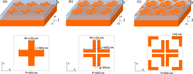
Figure 1 shows the schematic illustration and geometric parameters of three different structures for plasmonic light trapping and absorption enhancement in graphene. The metallic structures consist of arrays of periodical metallic crosses backed by a metallic mirror, which is a well-known design for plasmonic perfect absorbers39. From the top to the bottom of each structure are an array of metallic particles, the monolayer graphene, an insulator layer with a thickness of s = 80 nm and a metallic reflection mirror, respectively. The graphene film is in direct contact with the metallic crosses. The period is P = Px = Py = 550 nm. The insulator layer is assumed to be lossless with a refractive index of 1.5. The metallic crosses and mirror are made of gold. The thickness of the crosses are 30 nm. The incident light excites localized plasmons in the metallic structures, which trap light in the near-field and lead to strong absorption. As the graphene film is now integrated in the structures, a significant proportion of light will be absorbed by the graphene which will far exceed the absorption by a free standing graphene film.
Figure 1. Plasmonic absorbers for light trapping and absorption enhancement in graphene.
(a) Schematic of a plasmonic absorber comprising arrays of periodical metallic crosses backed by a metallic mirror. (b) A similar structure as in (a) but the metallic crosses have 20 nm wide cross gaps. (c) Schematic of a absorber consisting of two types of crosses with different dimensions to expand the absorption bandwidth. The top views of unit cells with geometric parameters are shown in the bottom.
First, we consider the structure in Fig. 1a. It consists of arrays of ordinary metallic crosses backed by a reflection mirror. This is a typical design for polarization-independent plasmonic perfect absorbers39,40. Figure 2 shows the numerically simulated absorption spectra under the illumination of a plane wave at normal incidence. Total absorption is shown in dashed line and absorption in the graphene is shown in solid line. It exhibits a single resonance in the studied spectral range. The inset shows the field distributions at the resonance. As is well known, an electric dipole mode is excited in the arm of the cross which forms a magnetic mode along with its image dipole by the reflection mirror. At the resonance wavelength of 1670 nm, the total absorption reaches about 93% while the absorption in the graphene is about 46%. As a reference, the absorption in a free standing monolayer graphene is also shown (the flat dashed black line). The resonant absorption in graphene is enhanced by 20 times with the plasmonic light trapping. The total absorption as well as absorption in graphene decreases as the wavelength of light is away from the resonant wavelength. Here the plasmonic resonance has a quality factor of about 5 and the graphene absorption keeps higher than 30% in a spectral band of about 280 nm (from the wavelength of 1546 nm to 1825 nm).
Figure 2. Absorption enhancement in graphene by plasmonic light trapping.
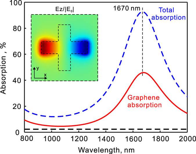
(a) Simulated spectra of total absorption (blue dashed line) as well as absorption in the graphene (red solid line) for the structure in Fig. 1a. The inset shows the field distributions at the resonance as denoted by the vertical dashed lines. The light is incident at normal direction with its electric field polarized along the x-direction. The field is plotted at the x–y plane that is 25 nm below the bottom surface of the gold crosses. The flat dashed line shows the absorption in a free standing graphene without enhancement.
Figure 3a shows simulated absorption spectra for the structure in Fig. 1b. The structure in Fig. 1b is similar to that in Fig. 1a but the metallic crosses have a 20 nm wide cross gap in the center. It exhibits two resonance peaks in the studied spectral range. At the resonance wavelength of 1560 nm, the total absorption and absorption in the graphene reach about 99.6% and 50%, respectively. The graphene absorption is enhanced by about 22 times at the resonance. The origin of this resonance is similar to the resonance in Fig. 2a as shown by the field distributions (see Fig. 3c and the inset in Fig. 2). Besides, there is an other resonance at about 985 nm with the total absorption and graphene absorption reaching 99.8% and 57%, respectively. This resonance is attributed to the excitation of a higher order mode as shown by the field distribution in Fig. 2b. So the introduction of a cross gap in the metallic cross can lead to dual resonant bands for absorption. Moreover, the middle gap could lead to field enhancements in the graphene plane which is beneficial for absorption enhancement in the graphene film.
Figure 3. Absorption enhancement in graphene by plasmonic light trapping with dual resonances.
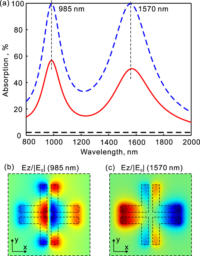
(a) Simulated spectra of total absorption (blue dashed line) as well as absorption in the graphene (red solid line) for the structure in Fig. 1b. The light is incident at normal direction with its electric field polarized along the x-direction. (b,c) show the field distributions at the two resonances as denoted in (a) by the vertical dashed lines. The field is plotted at the x–y plane that is 25 nm below the bottom surface of the gold crosses. The flat dashed lines show the absorption in a free standing graphene without enhancement.
Plasmonic resonators generally have an absorption cross-section bigger than its geometric size and multi-resonances can be realized by integrating two or more sub-resonators with different sizes in one unit cell39. Figure 4 shows the absorption spectra for the structure in Fig. 1c (solid red curves) as well as those for its two individual sub-structures (dash-dotted purple and dashed blue curves). The structure contains two crosses with different dimensions in each unit cell. The side width of the large cross is 400 nm (the side width of each L-shaped part is 190 nm and the gap width in the middle is 20 nm) and that of the small cross is 310 nm (the side width of each L-shaped part is 145 nm and the gap width in the middle is 20 nm). The combined structure exhibits four resonances in the studied spectral range including both the resonances of the small cross (dash-dotted purple curve) and resonances of the large cross (dashed blue curve). As a result, light trapping and strong absorption enhancement is now realized in a broadband wavelength range. The total absorption of the whole structure reaches more than 97% at the four resonances and exceeds 58% at range from 770 nm to 1740 nm (see Fig. 4a). At the same time, the light absorption in the monolayer graphene reaches more than 30% in an ultrabroad spectra range from 780 to 1760 nm (see Fig. 4a).
Figure 4. Broadband absorption enhancement in graphene by plasmonic light trapping.
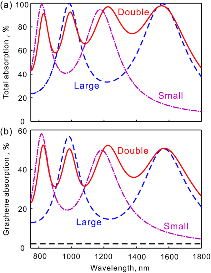
The solid red line shows the simulated spectra of absorption in the graphene for the structure in Fig. 1c. The absorption for the structures with just one type of crosses is described by the dashed blue line (large crosses) and dashed purple line (small crosses). The flat dashed line shows the absorption in a free standing graphene without enhancement.
In the above structures, the graphene film is in direct contact with the metallic crosses. This is just the case for many demonstrated graphene photodetectors34,35,36. Metals such as gold will lead to the change of graphene’s Fermi energy and get doped graphene41. The modification of the Fermi level is not limited only to graphene underneath the metal but also extends hundreds of nanometers into the uncovered graphene with varied doping levels42. Doping will affect the optical properties of graphene, particularly for light with photon energy around and below twice of the graphene’s Fermi energy15. According to previous study, the change of Fermi level induced by gold contact is generally less than 0.5 eV43. Even though metal-induced doping may lead to some decrease of absorption enhancement at the long wavelength range, broadband enhanced absorption can still be realized at visible and near infrared ranges.
Sometimes it may be necessary to have an insulator layer between the graphene film and the metallic plasmonic nanostructures (e.g., in order to protect the graphene film from unwanted doping and contamination). Figure 5 shows the absorption spectra of graphene with different separations between the graphene layer and metallic crosses. The inset in Fig. 5 shows the schematic cross section of the structure. The geometric parameters of the metallic crosses are just the same as in Fig. 1c. As is known, the metallic nanostructure here employs the typical design for plasmonic perfect absorbers and it forms a high impedance surface with the electric field mainly confines near the top surface (metallic crosses) of the structures. Not surprisingly, the absorption in graphene drops with the increase of the separation. As the separation is zero, the absorption in graphene is about 52.3%, 50.5%, 52.2%, 50.8% at the four resonances of 829 nm, 988 nm, 1225 nm, 1573 nm, respectively. As separation is s = 2 nm, the resonant absorption in graphene decreases to 41.8%, 40.2%, 39.6%, 38.8%, respectively. They drop to 32.4%, 31.7%, 30.9%, 30.7% at the separation of s = 5 nm and 10.4%, 11.3%, 12.6%, 13.3% at the separation of s = 20 nm. However, the absorption in graphene can still exceed 13.8% in the spectral range from 780 to 1800 nm when the separation is s = 5 nm.
Figure 5. Light absorption in graphene for different separations between the graphene layer and metallic crosses.
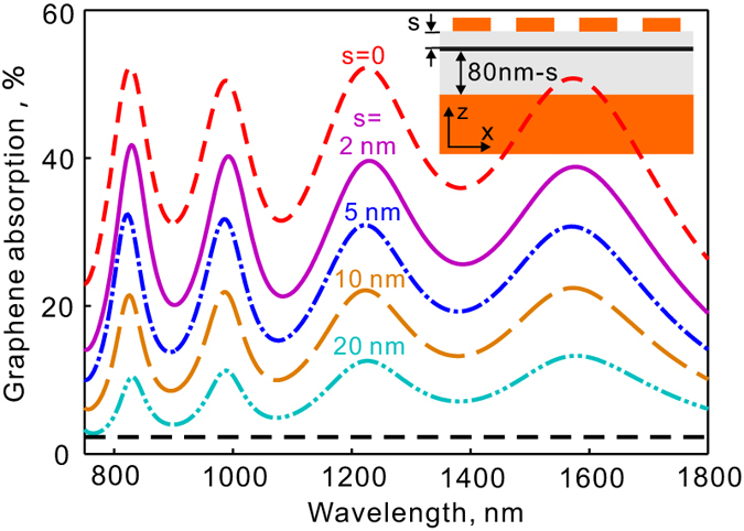
The separation varies from 0 to 20 nm. The separation layer is assumed to be lossless with a refractive index of 1.5. The flat dashed line shows the absorption in a free standing graphene without enhancement.
Besides monolayer graphene and other two-dimensional materials, heterostructures of two-dimensional materials with vertical stacks have attracted a great deal of attention for their potentials for optoelectronic applications. High-efficient and broadband photodetectors based on graphene double-layer heterostructures have been reported44,45. They consist of a pair of stacked graphene monolayers separated by a thin tunnel barrier. Our proposed structure can also be used for light trapping and graphene absorption enhancement in this type of devices. Figure 6 shows the absorption in a graphene double-layer heterostructure enhanced by plasmonic light trapping. The maximum absorption in the two graphene layers reaches about 62.6% (about 43.3% in the upper graphene layer and 19.3% in the lower layer) at the resonance of 1225 nm which is about 10% higher compared to the monolayer graphene. In the studied spectral range, the increase of absorption in graphene is slightly higher at longer wavelengths (about 10%) than that at shorter wavelengthes (about 5$ to 6%). This is due to the relatively larger spatial extensions of localized plasmonic fields near the metallic crosses at longer wavelengthes.
Figure 6. Broadband absorption enhancement in a graphene double layer by plasmonic light trapping.
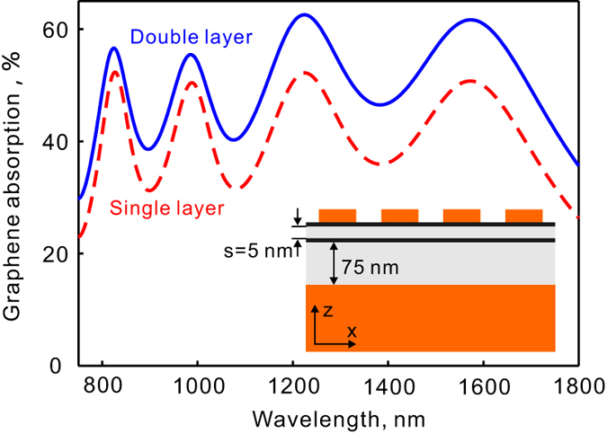
The two graphene monolayers are separated by a thin tunnel barrier with a thickness of 5 nm. The top layer of graphene is in contact with the metallic crosses. For simplicity, the separation layer is assumed to be lossless with a refractive index of 1.5.
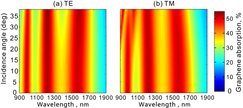
Figure 7 shows the angle dependence of absorption. Here the structure is the same as in Fig. 4. In order to avoid diffraction effects, we only consider wavelengthes from 900 to 1900 nm and the incident angle is below 39 degrees. As we see, the is a slight variation of absorption spectra under oblique incidence, particularly for p-polarized (TM) light where the resonance at the short wavelength splits at large incident angles. However, for both s-polarized (TE) and p-polarized (TM) light, the light absorption by monolayer graphene keeps higher than 27% in a spectral range from 900 to 1760 nm for incident angle up to 39 degrees.
Figure 7. Angle dependence of the resonant absorption in graphene for (a) s-polarized (TE) and (b) p-polarized (TM) light.
Here the graphene is in contact with the metallic crosses (s = 0) as in Fig. 1c.
Conclusions
In summary, we have numerically investigated three different plasmonic absorber designs for light trapping and absorption enhancement in graphene. The excitation of localized plasmons in the metallic structures can significantly enhance the interactions between graphene and light at the resonances. By employing a splitted cross design for plasmonic resonant antennas, dual resonances can be obtained in the studied spectral range. Furthermore, by integrating two types of sub-antennas with different sizes, the bandwidth for light trapping and absorption enhancement is effectively expanded due to multi-resonances. More than one order enhancement of optical absorption in a single layer graphene is realized in an unprecedented broad spectral range from 780 to 1760 nm. This enhancement functionality can be translated to any wavelength range from visible to terahertz by modifying the geometric design of the plasmonic structure and can be applied for other two dimensional materials and their heterogeneous structures. Besides, the proposed design is compact and suitable for integrated thin film devices which is an advantage over some other proposed methods for absorption enhancement in graphene46,47. The proposed metallic nanostructures can be fabricated by e-beam lithography, nano-imprint or other nano-fabrication techniques48,49. The designs may significantly improve the efficiency of optical devices such as broadband photodetectors and solar cells based on graphene and other two-dimensional materials.
Methods
The numerical simulations are conducted using a fully three-dimensional finite element technique (in Comsol MultiPhysics). In the simulation, the graphene is modelled as a conductive surface with an optical conductance of G0 = e2/(4ħ) ≈ 6.08 × 10⁻⁵ Ω−1 which corresponds to the absorption of about 2.3% for a free standing film. The permittivity of gold was described by the Drude model with plasma frequency ωp = 1.37 × 10¹⁶ s−1 and the damping constant ωτ = 1.23 × 10¹⁴ s−1 which was three times larger than the bulk value considering the increased scattering by surface and grain boundary effects in the thin film.
Additional Information
How to cite this article: Xiong, F. et al. Ultrabroadband, More than One Order Absorption Enhancement in Graphene with Plasmonic Light Trapping. Sci. Rep. 5, 16998; doi: 10.1038/srep16998 (2015).
Acknowledgments
The work is supported by National Undergraduate Innovative Training Program, National Natural Science Foundation of China (grant nos. 11304389, 61177051 and 61205087) and the National Basic Research Program of China (973 Program, grant no. 2012CB933501).
Footnotes
The authors declare no competing financial interests.
Author Contributions J.Z., Z.Z., X.Y. and S.Q. conceived the idea and supervised the study. F.X. and J.Z. conducted the numerical simulations. J.Z. wrote the manuscript. All authors contributed to the data analysis and reviewed the manuscript.
References
- Bonaccorso F., Sun Z., Hasan T. & Ferrari A. Graphene photonics and optoelectronics. Nat. Photonics 4, 611–622 (2010). [Google Scholar]
- Bao Q. & Loh K. P. Graphene photonics, plasmonics, and broadband optoelectronic devices. ACS Nano 6, 3677–3694 (2012). [DOI] [PubMed] [Google Scholar]
- Xia F., Wang H., Xiao D., Dubey M. & Ramasubramaniam A. Two-dimensional material nanophotonics. Nat. Photonics 8, 899–907 (2014). [Google Scholar]
- Wang X., Zhi L. & Müllen K. Transparent, conductive graphene electrodes for dye-sensitized solar cells. Nano Lett. 8, 323–327 (2008). [DOI] [PubMed] [Google Scholar]
- Bae S. et al. Roll-to-roll production of 30-inch graphene films for transparent electrodes. Nat. Nanotechnol. 5, 574–578 (2010). [DOI] [PubMed] [Google Scholar]
- Liu M. et al. A graphene-based broadband optical modulator. Nature 474, 64–67 (2011). [DOI] [PubMed] [Google Scholar]
- Bao Q. et al. Atomic-layer graphene as a saturable absorber for ultrafast pulsed lasers. Adv. Funct. Mater. 19, 3077–3083 (2009). [Google Scholar]
- Sun Z. et al. Graphene mode-locked ultrafast laser. ACS nano 4, 803–810 (2010). [DOI] [PubMed] [Google Scholar]
- Ju L. et al. Graphene plasmonics for tunable terahertz metamaterials. Nat. Nanotechnol. 6, 630–634 (2011). [DOI] [PubMed] [Google Scholar]
- Yan H. et al. Tunable infrared plasmonic devices using graphene/insulator stacks. Nat. Nanotechnol. 7, 330–334 (2012). [DOI] [PubMed] [Google Scholar]
- Zhu Z. et al. Electrically controlling the polarizing direction of a graphene polarizer. J. Appl. Phys. 116, 104304 (2014). [Google Scholar]
- Zhu Z. et al. Electrically tunable polarizer based on anisotropic absorption of graphene ribbons. Appl. Phys. A 114, 1017–1021 (2014). [Google Scholar]
- Koppens F. et al. Photodetectors based on graphene, other two-dimensional materials and hybrid systems. Nat. Nanotechnol. 9, 780–793 (2014). [DOI] [PubMed] [Google Scholar]
- Nair R. et al. Fine structure constant defines visual transparency of graphene. Science 320, 1308–1308 (2008). [DOI] [PubMed] [Google Scholar]
- Stauber T., Peres N. & Geim A. Optical conductivity of graphene in the visible region of the spectrum. Physical Review B 78, 085432 (2008). [Google Scholar]
- Xia F., Mueller T., Lin Y.-M., Valdes-Garcia A. & Avouris P. Ultrafast graphene photodetector. Nat. Nanotechnol. 4, 839–843 (2009). [DOI] [PubMed] [Google Scholar]
- Mueller T., Xia F. & Avouris P. Graphene photodetectors for high-speed optical communications. Nat. Photonics 4, 297–301 (2010). [Google Scholar]
- Furchi M. et al. Microcavity-integrated graphene photodetector. Nano Lett. 12, 2773–2777 (2012). [DOI] [PMC free article] [PubMed] [Google Scholar]
- Engel M. et al. Light–matter interaction in a microcavity-controlled graphene transistor. Nat. Commun. 3, 906 (2012). [DOI] [PMC free article] [PubMed] [Google Scholar]
- Gan X. et al. Strong enhancement of light–matter interaction in graphene coupled to a photonic crystal nanocavity. Nano Lett. 12, 5626–5631 (2012). [DOI] [PubMed] [Google Scholar]
- Piper J. R. & Fan S. Total absorption in a graphene monolayer in the optical regime by critical coupling with a photonic crystal guided resonance. ACS Photonics 1, 347–353 (2014). [Google Scholar]
- Gan X. et al. Chip-integrated ultrafast graphene photodetector with high responsivity. Nat. Photonics 7, 883–887 (2013). [Google Scholar]
- Wang X., Cheng Z., Xu K., Tsang H. K. & Xu J.-B. High-responsivity graphene/silicon-heterostructure waveguide photodetectors. Nat. Photonics 7, 888–891 (2013). [Google Scholar]
- Pospischil A. et al. Cmos-compatible graphene photodetector covering all optical communication bands. Nat. Photonics 7, 892–896 (2013). [Google Scholar]
- Chen J. et al. Optical nano-imaging of gate-tunable graphene plasmons. Nature 487, 77–81 (2012). [DOI] [PubMed] [Google Scholar]
- Fei Z. et al. Gate-tuning of graphene plasmons revealed by infrared nano-imaging. Nature 487, 82–85 (2012). [DOI] [PubMed] [Google Scholar]
- Koppens F. H., Chang D. E. & Garcia de Abajo F. J. Graphene plasmonics: a platform for strong light–matter interactions. Nano Lett. 11, 3370–3377 (2011). [DOI] [PubMed] [Google Scholar]
- Grigorenko A., Polini M. & Novoselov K. Graphene plasmonics. Nat. Photonics 6, 749–758 (2012). [Google Scholar]
- Zhang J., Zhu Z., Liu W., Yuan X. & Qin S. Towards photodetection with high efficiency and tunable spectral selectivity: graphene plasmonics for light trapping and absorption engineering. Nanoscale 7, 13530–13536 (2015). [DOI] [PubMed] [Google Scholar]
- Thongrattanasiri S., Koppens F. H. & de Abajo F. J. G. Complete optical absorption in periodically patterned graphene. Phys. Rev. Lett. 108, 047401 (2012). [DOI] [PubMed] [Google Scholar]
- Zhang J. et al. Coherent perfect absorption and transparency in a nanostructured graphene film. Opt. Express 22, 12524–12532 (2014). [DOI] [PubMed] [Google Scholar]
- Fang Z. et al. Gated tunability and hybridization of localized plasmons in nanostructured graphene. ACS Nano 7, 2388–2395 (2013). [DOI] [PubMed] [Google Scholar]
- Fang Z. et al. Active tunable absorption enhancement with graphene nanodisk arrays. Nano Lett. 14, 299–304 (2013). [DOI] [PubMed] [Google Scholar]
- Echtermeyer T. et al. Strong plasmonic enhancement of photovoltage in graphene. Nat. Commun. 2, 458 (2011). [DOI] [PubMed] [Google Scholar]
- Liu Y. et al. Plasmon resonance enhanced multicolour photodetection by graphene. Nat. Commun. 2, 579 (2011). [DOI] [PMC free article] [PubMed] [Google Scholar]
- Fang Z. et al. Graphene-antenna sandwich photodetector. Nano Lett. 12, 3808–3813 (2012). [DOI] [PubMed] [Google Scholar]
- Thackray B. D. et al. Super-narrow, extremely high quality collective plasmon resonances at telecom wavelengths and their application in a hybrid graphene-plasmonic modulator. Nano letters 15, 3519–3523 (2015). [DOI] [PubMed] [Google Scholar]
- Song S., Chen Q., Jin L. & Sun F. Great light absorption enhancement in a graphene photodetector integrated with a metamaterial perfect absorber. Nanoscale 5, 9615–9619 (2013). [DOI] [PubMed] [Google Scholar]
- Liu X. et al. Taming the blackbody with infrared metamaterials as selective thermal emitters. Phys. Rev. Lett. 107, 045901 (2011). [DOI] [PubMed] [Google Scholar]
- Liu X., Starr T., Starr A. F. & Padilla W. J. Infrared spatial and frequency selective metamaterial with near-unity absorbance. Phys. Rev. Lett. 104, 207403 (2010). [DOI] [PubMed] [Google Scholar]
- Reckinger N., Vlad A., Melinte S., Colomer J.-F. & Sarrazin M. Graphene-coated holey metal films: Tunable molecular sensing by surface plasmon resonance. Applied Physics Letters 102, 211108 (2013). [Google Scholar]
- Mueller T. et al. Role of contacts in graphene transistors: A scanning photocurrent study. Phys. Rev. B 79, 245430 (2009). [Google Scholar]
- Khomyakov P. et al. First-principles study of the interaction and charge transfer between graphene and metals. Physical Review B 79, 195425 (2009). [Google Scholar]
- Kim C. O. et al. High photoresponsivity in an all-graphene p–n vertical junction photodetector. Nat. Commun. 5, 3249 (2014). [DOI] [PubMed] [Google Scholar]
- Liu C.-H., Chang Y.-C., Norris T. B. & Zhong Z. Graphene photodetectors with ultra-broadband and high responsivity at room temperature. Nat. Nanotechnol. 9, 273–278 (2014). [DOI] [PubMed] [Google Scholar]
- Pirruccio G., Martín M. L., Lozano G. & Gómez R. J. Coherent and broadband enhanced optical absorption in graphene. ACS nano 7, 4810–4817 (2013). [DOI] [PubMed] [Google Scholar]
- Zhao W., Shi K. & Lu Z. Greatly enhanced ultrabroadband light absorption by monolayer graphene. Optics letters 38, 4342–4345 (2013). [DOI] [PubMed] [Google Scholar]
- Duan H., Hu H., Kumar K., Shen Z. & Yang J. K. Direct and reliable patterning of plasmonic nanostructures with sub-10-nm gaps. ACS nano 5, 7593–7600 (2011). [DOI] [PubMed] [Google Scholar]
- Duan H., Fernández-Domínguez A. I., Bosman M., Maier S. A. & Yang J. K. Nanoplasmonics: classical down to the nanometer scale. Nano Lett. 12, 1683–1689 (2012). [DOI] [PubMed] [Google Scholar]


