Abstract
Using helium atom scattering, we have studied the structure and dynamics of a graphene layer prepared in situ on a Ni(111) surface. Graphene/Ni(111) exhibits a helium reflectivity of ∼20% for a thermal helium atom beam and a particularly small surface electron density corrugation ((0.06 ± 0.02) Å peak to peak height). The Debye–Waller attenuation of the elastic diffraction peaks of graphene/Ni(111) and Ni(111) was measured at surface temperatures between 150 and 740 K. A surface Debye temperature of θD = (784 ± 14) K is determined for the graphene/Ni(111) system and θD = (388 ± 7) K for Ni(111), suggesting that the interlayer interaction between graphene and the Ni substrate is intermediary between those for strongly interacting systems like graphene/Ru(0001) and weakly interacting systems like graphene/Pt(111). In addition we present measurements of low frequency surface phonon modes on graphene/Ni(111) where the phonon modes of the Ni(111) substrate can be clearly observed. The similarity of these findings with the graphene/Ru(0001) system indicates that the bonding of graphene to a metal substrate alters the dynamic properties of the graphene surface strongly and is responsible for the high helium reflectivity of these systems.
Introduction
Metal–graphene interfaces are attracting much attention due to the possibility of synthesizing large area graphene films on metals by chemical vapor deposition.1 During deposition the metal substrate acts as a catalyst for the dehydrogenation of hydrocarbon precursors, which leaves carbon at the surface. The quality of graphene layers grown in this way is in general very high allowing us to investigate the elastic properties of these systems and the interaction strength between the graphene layer and the metallic substrate.2,3 Moreover, graphene–metal systems are excellent model systems in order to understand the interaction between organic semiconductors and metal electrodes which is vital in organic electronics.4 Since the interaction between an organic molecule and the substrate is weak compared with conventional metallic or covalent bonding, techniques such as X-ray scattering and high-energy electron diffraction can often turn out to be destructive. Neutral He atom beams with energies of typically 10 meV are perfectly suited to probe these systems in an inert, completely nondestructive manner.4−6 In addition, helium atom scattering (HAS) provides an accurate description of the surface charge density corrugation as seen by He atoms at thermal energies and the excellent surface sensitivity of this technique has been used to determine structural and vibrational properties of molecular adsorbates.4,5 More importantly, HAS can be used to obtain information about the weak interactions between substrates and a molecular overlayer: As recently shown by Shichibe et al.,4 by measuring the surface Debye temperature the interlayer bonding can be quantified, which is rather difficult to probe with other conventional techniques.
Graphene on Ni is considered to be one of the “strong binding” systems, like graphene/Ru(0001), while graphene/Pt(111) is a weakly binding system in which the graphene binding is about the same as it is for pure graphite.1,4 It has been suggested that graphene/Ni should be highly reflective to He atom scattering, because of its strong binding, similar to the case of graphene/Ru.5 Our measurements of the helium reflectivity and the Debye–Waller factor provide an excellent test of this theory.
Furthermore, we present measurements of the surface phonon modes in the very low energy regime which were previously limited to higher phonon energies in the case of graphene/Ni(111).1 These phonon modes hold important information about the thermal conductivity of graphene which is dominated by contributions from acoustic phonons near room temperature. It also shows the importance of the graphene–substrate interaction which has the potential to modify the corresponding phonon dispersion curves.
Experimental Details
All measurements of this work were conducted on the Cambridge helium-3 spin–echo apparatus.7 In this setup a nearly monochromatic beam of 3He is scattered of the sample surface in a fixed 44.4° source-target-detector geometry. Energy changes of the scattered He beam can be determined using the spin–echo principle. The setup of the whole apparatus has been described in greater detail elsewhere.7,8 The described measurements were carried out using an incident beam energy of 8 meV.
The Ni(111) single crystal used in the study was a disc with a diameter of 10 mm and a thickness of 1 mm. The crystal was mounted on the sample holder which can be heated using a radiative heating from a filament on the backside of the crystal or cooled down to 100 K using liquid nitrogen. The sample temperature was measured using a chromel–alumel thermocouple. Prior to the measurements, the surface was cleaned by Ar+ sputtering and annealing to 870 K.
Results and Discussion
Preparation and HAS from Graphene/Ni(111)
A monolayer of graphite on Ni(111) was grown by dosing ethene (C2H4) while heating the Ni crystal (730 K) over several hours.9,10 The resulting graphene layer is epitaxial and not rotated with respect to the substrate. The formation of a single domain of the graphitic lattice causes a diffraction pattern which exhibits the same symmetry as the hexagonal Ni(111) surface.
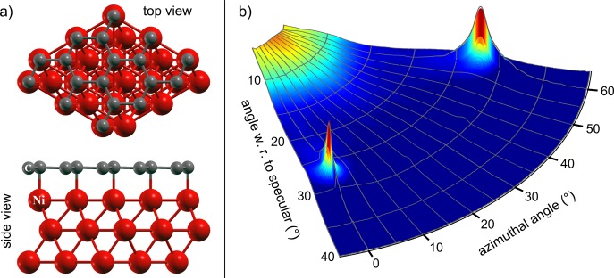
Figure 1 shows a three-dimensional polar plot of the scattered intensity from the prepared graphene/Ni(111) surface. Here the radial coordinate corresponds to the incident angle θi, and the polar angle corresponds to the azimuthal orientation of the crystal. The z-axis indicates the scattered intensity which is plotted on a logarithmic scale. One can clearly see the two diffraction peaks which are contained in the scanned azimuthal range. They are located at the same position as the peaks of the Ni substrate, hence suggesting a (1 × 1) structure on the underlying Ni(111) surface in accordance with prior studies.9,10
Figure 1.
(a) Top and side view of the graphene/Ni(111) surface structure (according to refs (10 and 11)). (b) Three-dimensional polar plot of the scattered He intensity for graphene/Ni(111) where the z-axis corresponds to the scattered intensity on a logarithmic scale. The scan was taken with an incident beam energy of Ei = 8 meV and the surface at 150 K. The two diffraction peaks which are contained in the scanned azimuthal range are clearly visible. The specular peak is not shown in the plot due the high intensity compared to the diffraction peaks.
Recent density functional theory (DFT) calculations suggest that the lowest energy configuration for graphene/Ni(111) is the top-fcc structure (see Figure 1a)) followed by the top-hcp structure which is less favorable.12−14 The energy difference between these two structures has been reported to be quite small, and domains with both configurations have been observed in experiments,13,14 even though Gamo et al. clearly favored the top-fcc structure.10 We are unable to distinguish the two configurations from our diffraction data. However, based on about 20% He reflectivity of the graphene covered surface and the small width of the specular peak, we expect to have predominantly one configuration since the number of defects and domain boundaries must be small in order to achieve this reflectivity.6
Note in particular that the specular reflectivity for He is comparable to the graphene/Ru(0001) system where a reflectivity of up to 23% was reported.5,15 Graphene/Ni(111) not only exhibits a high He reflectivity as recently predicted,5 its reflectivity remains also unchanged after O2 exposure at 2 × 10⁻⁷ mbar for 15 min similar to the graphene/Ru(0001) system.15 The reflectivity of the clean Ni(111) surface is ∼35% but Ni immediately starts picking up oxygen when exposed to O2, and its reflectivity decreases to almost 0 after the same exposure. By using the Debye–Waller factor which is determined later in this work, the reflectivity of graphene/Ni(111) measured at room temperature can be extrapolated to a reflectivity of ∼30% at 0 K.
Figure 2 displays the scattered intensity versus the incident angle θi for both Ni(111) and graphene/Ni(111) along the ΓM azimuth. On the graphene covered surface the intensity of the diffraction peak is increased by 2 orders of magnitude, indicating a larger corrugation of the surface electron density compared to the clean Ni(111) surface. According to the peak area, the intensity of the first order diffraction peak is only 0.003% of the specular intensity for Ni(111) and 1% for graphene/Ni(111), respectively.
Figure 2.
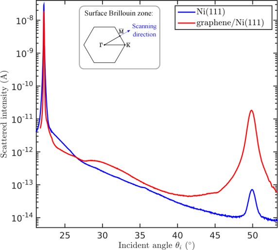
Comparison of the scattered intensities for graphene/Ni(111) and clean Ni(111) versus incident angle θi. Both scans were taken along the ΓM azimuth with the crystal at room temperature and a beam energy of 8 meV. The intensity of the diffraction peak is increased on the graphene covered surface which indicates a larger corrugation of the surface electron density compared to the pristine Ni surface. The inset shows the surface Brillouin zone and the scanning direction.
Using a purely elastic close-coupling calculation with a corrugated Morse potential,16 the peak-to-peak height of the surface electron density corrugation for graphene/Ni(111) is 2.5% of the Ni surface lattice constant and 0.22% in case of the pristine Ni surface, respectively. A calculation based on the eikonal approximation would give similar results. Hence the surface electron density corrugation for graphene/Ni(111) which corresponds to a peak to peak height of 0.06 Å is considerably larger than the one on clean Ni. However, it is still comparable to the findings of some metal surfaces6 and even smaller than the corrugation on graphite (0.21 Å17,18). Compared to graphene/Ru(0001) (0.15 Å19) and graphene/Rh(111) (0.9 Å20), this is the smallest surface electron density corrugation that has been reported for graphene/metal systems so far (see also Table 1).
Table 1. Comparison of the Surface Debye Temperatures and the Surface Charge Density Corrugation for Different Graphene/Metal Systems and Highly Oriented Pyrolytic Graphite (HOPG)a.
| surface Debye temperature (K) | electronic corrugation (Å) | |
|---|---|---|
| graphene/Ru(0001)15,19 | 1045 ± 25 | 0.15 |
| graphene/Ni(111) | 784 ± 14 | 0.06 |
| graphene/Pt(111)4 | 580 ± 70 | |
| HOPG4,17 | 480 ± 70 | 0.21 |
The values for graphene/Ni(111) have been determined within the framework of this study. The surface Debye temperature of graphene/Ni(111) lies between those for graphene/Ru(0001) and graphene/Pt(111). The electron density corrugation of graphene/Ni(111) is the smallest one of all listed systems (except for graphene/Pt(111) where no reported value for HAS exists to our knowledge).
Gamo et al.10 showed that the graphene ion cores have a very small corrugation of 0.05 Å in low energy electron diffraction (LEED) measurements. Scanning tunnelling microscopy (STM) measurements revealed an atomic corrugation of 0.1–0.15 Å for epitaxial graphene/Ni(111), which is roughly a factor of 3 larger than the height profile measured on bare Ni(111).21 A similar atomic corrugation with a peak-to-peak height of 0.2 Å is observed in STM measurements of moiré patterns that form in the case of a rotated graphene phase on Ni(111).1 When comparing values, it is important to remember that the corrugation determined by HAS is the surface charge density corrugation as seen by an 8 meV He beam.
The fact that the graphene covered surface has a larger electron density corrugation than the Ni(111) surface can also be used to monitor the graphene growth. Figure 3 shows how the intensity of the first order diffraction peak develops during growth. The intensity drops initially, upon formation of nickel carbide domains9 and later increases, upon conversion to graphene. The diffraction intensity saturates at a value above the initial intensity when the graphene layer is completed and the whole process terminates after a complete monolayer has been formed. The growth process itself is relatively slow and proceeds over a time scale of a few hours. However, this gives rise to very high quality graphene layers as also observed in previous studies, whereas at higher surface temperatures (>500 °C) rotated graphene phases are much more likely.9
Figure 3.
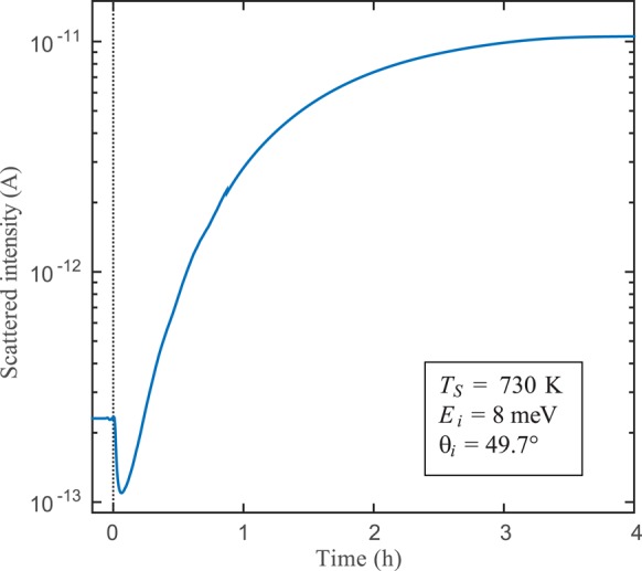
Growth of graphene on Ni(111) can be followed by monitoring the first order diffraction peak while dosing ethene (C2H4). Here the time t = 0 on the abscissa corresponds to starting the dosing of ethene. First nickel carbide forms and the intensity drops. As soon as this converts to graphene, the intensity increases since graphene exhibits a larger corrugation than Ni(111). The whole growth process continues over several hours.
Surface Debye Temperatures
The thermal attenuation of the diffraction peaks provides information about both the surface vibrational dynamics as well as the bonding strength of the graphene layer to the underlying substrate.4 The onset of thermal vibrations of the surface atoms at finite temperatures causes inelastic scattering of the incoming particles. This can be observed in the thermal attenuation of the coherent diffraction intensities whereupon the peak shape does not change.6
The inset in Figure 4 shows the decay of the zero order peak for He scattered from graphene/Ni(111) at an incident beam energy Ei = 8 meV. Scans of the scattered intensity versus the incident angle θi were collected, while the crystal temperature was varied between 150 and 740 K. The decay of the peak intensity with increasing surface temperature TS is caused by the increasing vibrational amplitude of the surface oscillators, which can be described by the Debye–Waller factor. The Debye–Waller factor exp[−2W(TS) ] relates the diffraction intensity I(TS) of a sample at temperature TS to the intensity I0 of a sample at rest by6
| 1 |
The Debye–Waller factor is described using
| 2 |
where u, is the displacement of a lattice atom out of its equilibrium position and Δk the momentum transfer. Here, the outer brackets denote the thermal average.6Equation 2 can be decomposed into contributions from perpendicular momentum transfer Δkz and parallel momentum transfer |ΔK|:22,23
| 3 |
For elastic scattering the momentum transfer is given by |ΔK | = |ki| (sin(θi) – sin(θf)) with the incident wave vector ki and θi and θf the incident and final angle with respect to the surface normal, respectively. Assuming that the momentum transfer parallel to the surface is zero (i.e., for the specular geometry θi = θf) eq 3 reduces to
| 4 |
with ⟨uz2⟩, the average square displacement of a crystal atom perpendicular to the surface. When using the relation 1/2Mω2⟨u2⟩ = 3/2kBT for a classical harmonic oscillator and applying the Debye model with the definition of the Debye temperature24 in terms of the Debye frequency ωD: ℏωD/kBT = θD/T, eq 4 becomes
| 5 |
where M is the mass of the surface atom and θD the surface Debye temperature.
Figure 4.
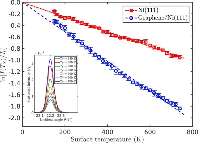
Decay of the logarithmic specular peak intensity ln[I(TS)] versus surface temperature TS using an incident beam energy of 8 meV for the Ni(111) surface and for graphene/Ni(111). In the inset, scans over the specular peak of graphene/Ni(111) are depicted for a couple of different temperatures.
It should be noted that eq 5 is not generally valid and problems arise in the application to atom-surface scattering due to the relatively long-range of the interaction potential and because the collisions are often no longer fast enough to be considered impulsive.25−27 Levi and Suhl28 have proposed corrections that account for the long interaction time with respect to the vibrational phonon periods and the presence of the attractive atom–surface interaction can be included using the Beeby correction.29 The first correction requires the knowledge of the surface phonon spectrum and is rather involved. Since we are dealing with comparatively small parallel momentum transfers (8 meV beam) in the presented HAS experiments, eq 5 can be considered to be approximately correct6,15,30,31 and will form the basis for the following analysis. The latter correction is accounted for as described in the following.
The attractive part of the atom–surface interaction potential can be taken into account by using the Beeby correction. Because of the attractive part of the potential, the incoming He atoms are first accelerated, and the scattered atoms are then decelerating as they leave the surface. Consequently, this effect of the attractive well is considered by replacing the perpendicular momentum transfer Δkz by6,30
| 6 |
which assumes an attractive part of the potential with a spatially uniform well of depth D, where values in the range of 4–16 meV are typical for HAS.6
In the case of the specular geometry, θi = θf holds and the Debye–Waller factor (eq 5) together with the Beeby correction simplifies to
| 7 |
where m is the impinging particle mass and the momentum is now replaced by the incident beam energy Ei using ki2 = 2m Ei/ℏ2.
According to eq 1, a plot of the natural logarithm of the intensity ln[I(TS)/I0]versus the surface temperature TS gives rise to a linear decay within the Debye model whereupon the surface Debye temperature can be calculated from the slope. Figure 4 shows the decay of the specular peak intensity versus the surface temperature for both graphene/Ni(111) and the pristine Ni(111) surface.
Equation 7, together with eq 1, is used to determine the surface Debye temperature (θD) from the experimental data. The potential well depth D for graphite and graphene/metal systems is typically 15–16 meV,4,17,32 and, in the present analysis, we used a value of 15.7 meV.32 (The sensitivity of the Debye temperature θD to changing D by 1 meV is relatively small and falls within the experimental uncertainty of θD.) While there are no reported values for Ni(111) in the literature, D has been determined to be 6.6 meV for Cu(111) and 7 meV for Ag(111).33 Hence we have used D = 6.6 meV, assuming that the well depth is similar to that of Cu(111).
One must also assume a value for the mass M which is typically the mass of the crystal atoms since the surface Debye temperature and vibration amplitudes are usually related to the motion of the ion cores. However, He atoms are scattered by the electron density; i.e., in the case of inelastic scattering this corresponds to a scattering by phonon-induced charge density oscillations.34,35 While the association of these charge density oscillations with the surface Debye temperature is possible due to the electron–phonon coupling the value for M is not necessarily the mass of a single atom.4
Recently it has been suggested that the Debye–Waller factor in atom scattering is better expressed in terms of the electron–phonon interaction parameters for simple metal surfaces.36 This approach has the advantage that it does not include the mass of the surface scatterer. However, the method has not been extended to more complicated surfaces than simple metals so far. Moreover, even though there is some ambiguity connected with the mass of the surface scatterer, these simple equations have proven to serve as a good approximation in the case of HAS,6,15,30 and using the mass of a single surface atom is a reasonable choice in most cases.4,15
Using the best-fit results a surface Debye temperature θD = (784 ± 14) K is obtained for the graphene/Ni(111) system and θD = (388 ± 7) K for Ni(111). Here we have set M in eq 7 equal to the mass of a single carbon or nickel atom, respectively. In Table 1 the surface Debye temperatures for various graphene/metal systems and for highly oriented pyrolytic graphite (HOPG) are listed in descending order. The surface Debye temperature for graphene/Ni can be found in a region that is between the values found for strongly interacting graphene (graphene/Ru(0001)4,15) and weakly interacting graphene (graphene/Pt(111)4). While the low surface electron density corrugation suggests an interaction with the Ni(111) substrate that is not large enough to cause any rippling of the graphene layer, it is still greater than for weakly interacting systems, hence explaining the high He reflectivity.
In the case of Ni(111) the surface Debye temperature has been determined with LEED previously, yielding a value of θD = (370 ± 5) K.37 Even though precaution must be taken when comparing HAS measurements with LEED experiments due to the different nature of the scattering processes, our findings are in very good agreement with the value obtained from LEED.
In order to confirm the consistency of our measurements, we apply the same analysis to the first order diffraction peaks measured along the ΓM azimuth. A plot of ln[I(TS)] versus the surface temperature TS for the first order diffraction peak is depicted in Figure 5. Using the slope of the linear fits, the Debye temperature can be calculated using eq 5. Since the mirror condition θi = θf no longer holds, the perpendicular momentum transfer is calculated using eq 6 with the same parameters for the well depth as before.
Figure 5.
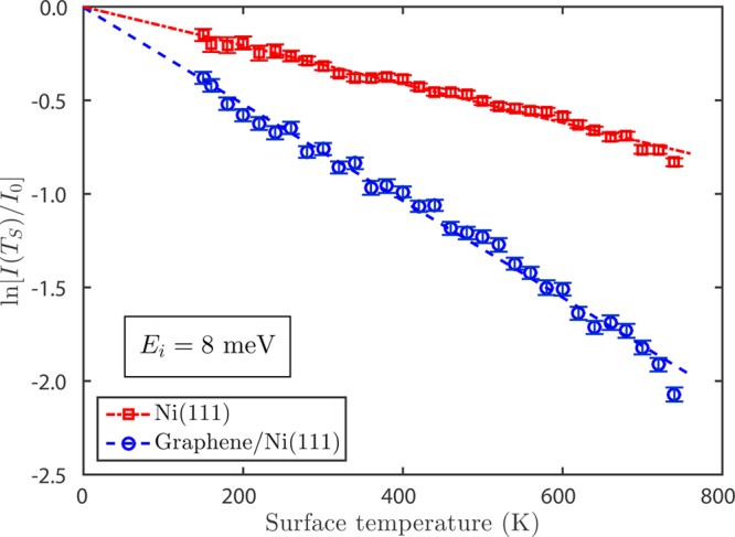
Decay of the logarithmic peak intensity ln[I(TS)] with increasing surface temperature TS of the first order diffraction peak along ΓM. The plot shows the decay for both Ni(111) and graphene/Ni(111), measured at an incident beam energy of 8 meV.
The surface Debye temperature from the analysis of the first order diffraction peak intensities is θD = (760 ± 30) K for graphene/Ni(111) and θD = (410 ± 22) K for Ni(111). Both values are in very good agreement with the Debye temperatures determined from the specular peak.
Phonon Spectra for Graphene/Ni(111)
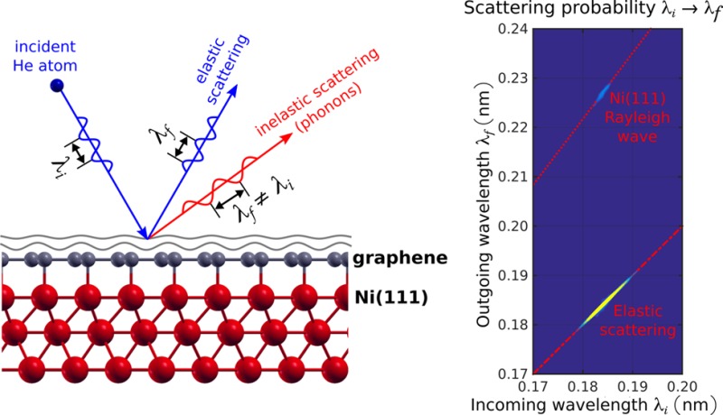
The phonon spectra which have been recorded along the ΓM azimuth suggest that there is no significant difference in the surface phonon dispersion relation for Ni(111) and the graphene covered surface within the energy range accessible with a 8 meV beam. In Figure 6 the 2D wavelength intensity matrix8 for graphene/Ni(111) at an incident angle of 18.2° is displayed with λi being the incident wavelength and λf the final wavelength, respectively. The only noticeable feature except for the elastic peak at λf = λi is the Rayleigh mode of Ni(111) on the phonon creation side (at larger λf).
Figure 6.
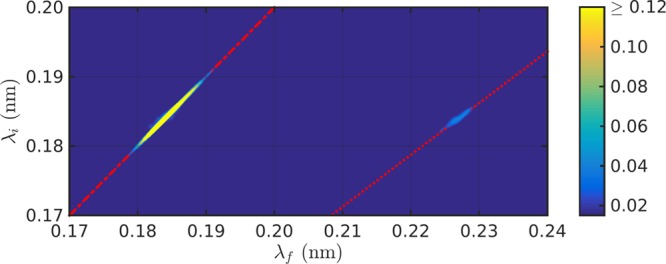
2D wavelength intensity matrix for graphene/Ni(111) along ΓM recorded at θi = 18.2°, a beam energy of 8 meV, and a sample temperature of 150 K. The plot shows the measured probability for detecting a scattered He atom with wavelength λf versus the incoming wavelength λi (see refs (8 and 38) for details). The only two visible features are the elastic peak (at λf = λi) and the Rayleigh mode on the creation side (at larger λf). This is also highlighted by the red dash-dotted line which corresponds to elastic scattering (λf = λi) and the red dotted line which corresponds to the phonon dispersion of the Rayleigh wave of Ni(111).
At first glance, one might expect to detect phonon modes similar to the ones in graphite39,40 or graphene41,42 on graphene/Ni(111). The three acoustic modes (ZA, TA, and LA) should be at a detectable energy within the vicinity of the Γ-point. However, previous measurements of the graphene/Ni have only covered phonon events at energies greater than 20 meV.1,2,43,44 The experiments in the present work have been performed for in plane scattering along the ΓM azimuth of the crystal. For this geometry, the scattering plane, defined by the incoming and scattered He beam, coincides with a mirror plane of the surface. Hence the TA mode cannot be excited since it is antisymmetric with respect to the scattering plane.45,46 As shown by de Juan et al.,45 the symmetry is not broken by bonding of the graphene layer to the substrate in the case of Ni(111). However, because of the bonding to a perfectly commensurate triangular substrate the ZA mode becomes much stiffer for wavevectors close to Γ lifting its energies to values above 20 meV,45 which brings the ZA mode out of the detectable energy range of our instrument.
Hence the LA mode is the only phonon mode present in graphene/Ni(111) that is experimentally accessible within the framework of the present study. The LA mode has the largest slope of the acoustic phonon modes and would only be detectable close to Γ. While in the current spectra there are no indications for this mode, it would require a more thorough investigation at specific scattering conditions to make any final conclusions since low energy phonon modes have been found on other graphene/metal systems.3,5,47 Nevertheless, an important result of this study is that the Rayleigh mode and the longitudinal resonance of the Ni(111) substrate48,49 are observable on the graphene covered surface, even though the Ni atoms are screened out by the graphene sheet.
A typical phonon spectrum is shown in Figure 7 together with a spectrum taken on Ni(111) under the same experimental conditions. Both spectra have been normalized by the area under each individual spectrum. This is based on the fact that the overall scattered intensities including elastic scattering due to static defects and inelastic scattering are roughly the same on both surfaces at this incident angle. We have investigated other normalization methods and ensured that our conclusions are robust. In Figure 7 the Rayleigh mode and the longitudinal resonance can be seen on the creation side. The intensity of the Rayleigh mode is clearly reduced on the graphene covered surface with respect to the intensity on Ni(111). The same trend can be seen when comparing intensities of several spectra throughout the ΓM direction.
Figure 7.
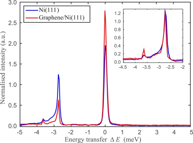
Comparison of the phonon spectra for graphene/Ni(111) and Ni(111). The spectrum was taken along the ΓM azimuth at an incident angle θi = 18.2°, Ei = 8 meV, and the sample was cooled down to 150 K. Both spectra have been normalized by the area under each spectrum. Despite the diffuse elastic peak at 0 energy transfer, both the Rayleigh mode at −2.7 meV and the longitudinal resonance at −3.6 meV can clearly be seen. The intensity of the Rayleigh mode is smaller on the graphene covered surface. In the inset the spectrum of the graphene covered surface has been scaled so that the Rayleigh mode exhibits the same height as on the pristine surface. This illustrates that the scattering cross section for the longitudinal resonance at −3.6 meV is enhanced with respect to the intensity of the Rayleigh mode on the graphene covered surface.
As we are observing low frequency phonon modes, i.e., long wavelength modes, one would expect that the whole graphene layer can move up and down with the Ni substrate since the graphite atoms are much lighter than the Ni atoms, provided a relatively strong bonding to the substrate. Note in our experiment it is difficult to obtain an absolute experimental ratio of the phonon cross-section in graphene and nickel. The fact that the static electron density corrugation is significantly different will certainly affect the phonon intensities. However, there are also important changes in the relative intensities of the two main phonon modes. The inset in Figure 7 shows that the scattering cross section of the longitudinal resonance seems to be enhanced on the graphene covered surface when related to the intensity of the Rayleigh mode.
Since this mode appears at higher energies (and smaller momentum transfer) compared to the Rayleigh mode, the so-called “quantum sonar” effect50 may play an important role: By this we mean that inelastic scattering of He atoms is due to phonon-induced charge density oscillations with subsurface phonon modes being made accessible due to the electron–phonon coupling. The electron–phonon coupling parameters λ found for graphite and graphene/metal systems have been reported to be close to 1,51 which is similar to values reported for other systems where subsurface phonon modes could be detected with HAS.35,52
Furthermore, the observation of the Rayleigh mode from the substrate is consistent with measurements of graphene/Ru(0001) where a strong intensity of the Rayleigh mode from the Ru(0001) substrate was found.5 Maccariello at el. demonstrated that surface charge density oscillations are the main contribution for this observation on graphene/Ru, although the graphene layer also oscillates with the underlying Ru surface due to the strong bonding to the substrate.5
Summary and Conclusion
Graphene/Ni(111) was prepared under ultrahigh vacuum conditions and studied using helium-3 spin–echo spectroscopy. The epitaxial graphene layer exhibits an electron density corrugation with a peak to peak height of 0.06 Å upon scattering of 3He with a beam energy of 8 meV. This corrugation is smaller than the values reported for graphene/Ru(0001) (0.15 Å) and graphite (0.21 Å). The graphene/Ni(111) surface shows a high He reflectivity of ∼20%, similar to the value reported for graphene/Ru(0001).
The thermal attenuation in the diffraction of He from graphene/Ni(111) and Ni(111) was studied in a temperature range between 150 and 740 K. Both systems show a typical Debye–Waller behavior and a surface Debye temperature of θD = (784 ± 14) K is determined for the graphene/Ni(111) system and θD = (388 ± 7) K for Ni(111). The surface Debye temperature for graphene/Ni(111) lies between those for strongly interacting systems (graphene/Ru(0001)) and weakly interacting systems (graphene/Pt(111)).
Measurements of the surface phonon modes in the low energy region show the same modes as on the pristine Ni surface. Two of the three acoustic phonon modes of graphene are not accessible in our setup. The observation of the Ni(111) surface modes can be explained in terms of a relatively strong binding to the substrate and the lighter mass of the graphite atoms compared to the substrate. In addition, the ability of HAS to detect subsurface phonon modes due to the electron–phonon coupling can also enhance the scattered intensity from these substrate modes, even though the Ni substrate is covered by the graphene monolayer. In general, the intensity of the Rayleigh mode is smaller on the graphene coated surface compared to the Ni surface.
Our findings confirm that graphene/Ni(111) can be created with very high quality and forms an ideal support system for the study of interactions between metals, carbon, and eventually adsorbate atoms. The similarity of our results with atom scattering results from graphene/Ru5 perfectly confirms the theory that graphene–metal systems with a relatively strong bonding to the substrate should give rise to a high He reflectivity.
Acknowledgments
The authors would like to thank Robert Weatherup and Daniel Farías for their advice on the graphene growth procedure. The authors are also grateful to J. R. Manson for many helpful discussions. One of us (A.T.) acknowledges financial support provided by the FWF (Austrian Science Fund) within the Project J3479-N20. E.B. would like to thank the Ecole Doctorale de Physique of the Université de Grenoble for funding.
The authors declare no competing financial interest.
References
- Dahal A.; Batzill M. Graphene-nickel interfaces: a review. Nanoscale 2014, 6, 2548–2562 10.1039/c3nr05279f. [DOI] [PubMed] [Google Scholar]
- Allard A.; Wirtz L. Graphene on metallic substrates: suppression of the Kohn anomalies in the phonon dispersion. Nano Lett. 2010, 10, 4335–4340 10.1021/nl101657v. [DOI] [PubMed] [Google Scholar]
- Politano A.; Marino A. R.; Chiarello G. Phonon dispersion of quasi-freestanding graphene on Pt(111). J. Phys.: Condens. Matter 2012, 24, 104025. 10.1088/0953-8984/24/10/104025. [DOI] [PubMed] [Google Scholar]
- Shichibe H.; Satake Y.; Watanabe K.; Kinjyo A.; Kunihara A.; Yamada Y.; Sasaki M.; Hayes W. W.; Manson J. R. Probing interlayer interactions between graphene and metal substrates by supersonic rare-gas atom scattering. Phys. Rev. B: Condens. Matter Mater. Phys. 2015, 91, 155403. 10.1103/PhysRevB.91.155403. [DOI] [Google Scholar]
- Maccariello D.; Campi D.; Al Taleb A.; Benedek G.; Farías D.; Bernasconi M.; Miranda R. Low-energy excitations of graphene on Ru(0001). Carbon 2015, 93, 1–10 10.1016/j.carbon.2015.05.028. [DOI] [Google Scholar]
- Farías D.; Rieder K.-H. Atomic beam diffraction from solid surfaces. Rep. Prog. Phys. 1998, 61, 1575. 10.1088/0034-4885/61/12/001. [DOI] [Google Scholar]
- Jardine A.; Hedgeland H.; Alexandrowicz G.; Allison W.; Ellis J. Helium-3 spin-echo: principles and application to dynamics at surfaces. Prog. Surf. Sci. 2009, 84, 323. 10.1016/j.progsurf.2009.07.001. [DOI] [Google Scholar]
- Alexandrowicz G.; Jardine A. P. Helium spin-echo spectroscopy: studying surface dynamics with ultra-high-energy resolution. J. Phys.: Condens. Matter 2007, 19, 305001. 10.1088/0953-8984/19/30/305001. [DOI] [Google Scholar]
- Patera L. L.; Africh C.; Weatherup R. S.; Blume R.; Bhardwaj S.; Castellarin-Cudia C.; Knop-Gericke A.; Schloegl R.; Comelli G.; Hofmann S.; et al. In situ observations of the atomistic mechanisms of Ni catalyzed low temperature graphene growth. ACS Nano 2013, 7, 7901–7912 10.1021/nn402927q. [DOI] [PubMed] [Google Scholar]
- Gamo Y.; Nagashima A.; Wakabayashi M.; Terai M.; Oshima C. Atomic structure of monolayer graphite formed on Ni(111). Surf. Sci. 1997, 374, 61–64 10.1016/S0039-6028(96)00785-6. [DOI] [Google Scholar]
- Wintterlin J.; Bocquet M.-L. Graphene on metal surfaces. Surf. Sci. 2009, 603, 1841–1852 10.1016/j.susc.2008.08.037. [DOI] [Google Scholar]
- Bianchini F.; Patera L. L.; Peressi M.; Africh C.; Comelli G. Atomic scale identification of coexisting graphene structures on Ni(111). J. Phys. Chem. Lett. 2014, 5, 467–473 10.1021/jz402609d. [DOI] [PubMed] [Google Scholar]
- Zhang W.-B.; Chen C.; Tang P.-Y. First-principles study for stability and binding mechanism of graphene/Ni(111) interface: Role of vdW interaction. J. Chem. Phys. 2014, 141, 044708. 10.1063/1.4890728. [DOI] [PubMed] [Google Scholar]
- Parreiras D. E.; Soares E. A.; Abreu G. J. P.; Bueno T. E. P.; Fernandes W. P.; de Carvalho V. E.; Carara S. S.; Chacham H.; Paniago R. Graphene/Ni(111) surface structure probed by low-energy electron diffraction, photoelectron diffraction, and first-principles calculations. Phys. Rev. B: Condens. Matter Mater. Phys. 2014, 90, 155454. 10.1103/PhysRevB.90.155454. [DOI] [Google Scholar]
- Politano A.; Borca B.; Minniti M.; Hinarejos J. J.; Vázquez de Parga A. L.; Farías D.; Miranda R. Helium reflectivity and Debye temperature of graphene grown epitaxially on Ru(0001). Phys. Rev. B: Condens. Matter Mater. Phys. 2011, 84, 035450. 10.1103/PhysRevB.84.035450. [DOI] [Google Scholar]
- Mayrhofer-Reinhartshuber M.; Kraus P.; Tamtögl A.; Miret-Artés S.; Ernst W. E. Helium-surface interaction potential of Sb(111) from scattering experiments and close-coupling calculations. Phys. Rev. B: Condens. Matter Mater. Phys. 2013, 88, 205425. 10.1103/PhysRevB.88.205425. [DOI] [Google Scholar]
- Boato G.; Cantini P.; Tatarek R. Study of gas-graphite potential by means of helium atom diffraction. Phys. Rev. Lett. 1978, 40, 887–889 10.1103/PhysRevLett.40.887. [DOI] [Google Scholar]
- Oh J. P.; Kondo T.; Hatake D.; Nakamura J. Elastic and inelastic scattering components in the angular intensity distribution of He scattered from graphite. Surf. Sci. 2009, 603, 895–900 10.1016/j.susc.2009.02.007. [DOI] [Google Scholar]
- Borca B.; Barja S.; Garnica M.; Minniti M.; Politano A.; Rodriguez-García J. M.; Hinarejos J. J.; Farías D.; Parga A. L. V. d.; Miranda R. Electronic and geometric corrugation of periodically rippled, self-nanostructured graphene epitaxially grown on Ru(0001). New J. Phys. 2010, 12, 093018. 10.1088/1367-2630/12/9/093018. [DOI] [Google Scholar]
- Gibson K.; Sibener S. J. Helium atom scattering from graphene grown on Rh(111). J. Phys. Chem. C 2014, 118, 29077–29083 10.1021/jp504024t. [DOI] [Google Scholar]
- Dzemiantsova L. V.; Karolak M.; Lofink F.; Kubetzka A.; Sachs B.; von Bergmann K.; Hankemeier S.; Wehling T. O.; Frömter R.; Oepen H. P.; Lichtenstein A. I.; Wiesendanger R.; et al. Multiscale magnetic study of Ni(111) and graphene on Ni(111). Phys. Rev. B: Condens. Matter Mater. Phys. 2011, 84, 205431. 10.1103/PhysRevB.84.205431. [DOI] [Google Scholar]
- Bracco G.; Ward M. D.; Scoles G. Atomic diffraction study of the interaction of helium atoms with the surface of an organic single crystal: The (001) cleavage planes of guanidinium methanesulfonate. J. Chem. Phys. 2003, 118, 8405. 10.1063/1.1566934. [DOI] [Google Scholar]
- Lapujoulade J.; Perreau J.; Kara A. The thermal attenuation of elastic scattering of helium from copper single crystal surfaces. Surf. Sci. 1983, 129, 59. 10.1016/0039-6028(83)90094-8. [DOI] [Google Scholar]
- Kittel C.Introduction to Solid State Physics; John Wiley & Sons Inc: New York, 2005. [Google Scholar]
- Gumhalter B. Different aspects of the Debye-Waller factor in various atom-surface scattering theories. Surf. Sci. 1996, 347, 237–248 10.1016/0039-6028(95)00954-X. [DOI] [Google Scholar]
- Siber A.; Gumhalter B. Debye-Waller factor in He-Cu(001) collisions revisited: the role of the interaction potentials. Surf. Sci. 1997, 385, 270–280 10.1016/S0039-6028(97)00194-5. [DOI] [Google Scholar]
- Daon S.; Pollak E.; Miret-Artés S. Communication: Semiclassical perturbation theory for the quantum diffractive scattering of atoms on thermal surfaces. J. Chem. Phys. 2012, 137, 201103. 10.1063/1.4768227. [DOI] [PubMed] [Google Scholar]
- Levi A. C.; Suhl H. Quantum theory of atom-surface scattering: Debye-Waller factor. Surf. Sci. 1979, 88, 221–254 10.1016/0039-6028(79)90577-6. [DOI] [Google Scholar]
- Beeby J. L. The scattering of helium atoms from surfaces. J. Phys. C: Solid State Phys. 1971, 4, L359–L362 10.1088/0022-3719/4/18/001. [DOI] [Google Scholar]
- Becker J. S.; Brown R. D.; Johansson E.; Lewis N. S.; Sibener S. J. Helium atom diffraction measurements of the surface structure and vibrational dynamics of CH3-Si(111) and CD3-Si(111) surfaces. J. Chem. Phys. 2010, 133, 104705. 10.1063/1.3483465. [DOI] [PubMed] [Google Scholar]
- Tamtögl A.; Mayrhofer-Reinhartshuber M.; Kraus P.; Ernst W. E. Surface Debye temperature and vibrational dynamics of antimony(111) from helium atom scattering measurements. Surf. Sci. 2013, 617, 225–228 10.1016/j.susc.2013.08.001. [DOI] [Google Scholar]
- Boato G.; Cantini P.; Salvo C.; Tatarek R.; Terreni S. Atomic vibrations at the (0001) graphite surface studied by He atom scattering. Surf. Sci. 1982, 114, 485–497 10.1016/0039-6028(82)90700-2. [DOI] [Google Scholar]
- Eichenauer D.; Harten U.; Toennies J. P.; Celli V. Interaction potential for one-phonon inelastic He-Cu(111) and He-Ag(111) scattering. J. Chem. Phys. 1987, 86, 3693–3710 10.1063/1.451972. [DOI] [Google Scholar]
- Benedek G.; Bernasconi M.; Chis V.; Chulkov E.; Echenique P. M.; Hellsing B.; Toennies J. P. Theory of surface phonons at metal surfaces: recent advances. J. Phys.: Condens. Matter 2010, 22, 084020. 10.1088/0953-8984/22/8/084020. [DOI] [PubMed] [Google Scholar]
- Tamtögl A.; Kraus P.; Mayrhofer-Reinhartshuber M.; Campi D.; Bernasconi M.; Benedek G.; Ernst W. E. Surface and subsurface phonons of Bi(111) measured with helium atom scattering. Phys. Rev. B: Condens. Matter Mater. Phys. 2013, 87, 035410. 10.1103/PhysRevB.87.035410. [DOI] [Google Scholar]
- Manson J. R.; Benedek G.; Miret-Artés S.. A new approach to atom scattering from conducting surfaces, unpublished 2015.
- Krupski A. Debye temperature of the Pb layers on Ni(111). Phys. Status Solidi B 2006, 243, 467–472 10.1002/pssb.200541219. [DOI] [Google Scholar]
- Kole P. R.; Jardine A. P.; Hedgeland H.; Alexandrowicz G. Measuring surface phonons with a 3He spin echo spectrometer: a two-dimensional approach. J. Phys.: Condens. Matter 2010, 22, 304018. 10.1088/0953-8984/22/30/304018. [DOI] [PubMed] [Google Scholar]
- Benedek G.; Brusdeylins G.; Heimlich C.; Toennies J.; Valbusa U. Surface phonons in graphite (001). Surf. Sci. 1986, 178, 545–552 10.1016/0039-6028(86)90331-6. [DOI] [Google Scholar]
- Oshima C.; Aizawa T.; Souda R.; Ishizawa Y.; Sumiyoshi Y. Surface phonon dispersion curves of graphite (0001) over the entire energy region. Solid State Commun. 1988, 65, 1601–1604 10.1016/0038-1098(88)90660-6. [DOI] [Google Scholar]
- Yan J.-A.; Ruan W. Y.; Chou M. Y. Phonon dispersions and vibrational properties of monolayer, bilayer, and trilayer graphene: Density-functional perturbation theory. Phys. Rev. B: Condens. Matter Mater. Phys. 2008, 77, 125401. 10.1103/PhysRevB.77.125401. [DOI] [Google Scholar]
- Michel K. H.; Verberck B. Theory of the evolution of phonon spectra and elastic constants from graphene to graphite. Phys. Rev. B: Condens. Matter Mater. Phys. 2008, 78, 085424. 10.1103/PhysRevB.78.085424. [DOI] [Google Scholar]
- Shikin A.; Farías D.; Adamchuk V.; Rieder K.-H. Surface phonon dispersion of a graphite monolayer adsorbed on Ni(111) and its modification caused by intercalation of Yb, La and Cu layers. Surf. Sci. 1999, 424, 155–167 10.1016/S0039-6028(99)00099-0. [DOI] [Google Scholar]
- Aizawa T.; Souda R.; Ishizawa Y.; Hirano H.; Yamada T.; Tanaka K.-I.; Oshima C. Phonon dispersion in monolayer graphite formed on Ni(111) and Ni(001). Surf. Sci. 1990, 237, 194–202 10.1016/0039-6028(90)90531-C. [DOI] [Google Scholar]
- de Juan F.; Politano A.; Chiarello G.; Fertig H. A. Symmetries and selection rules in the measurement of the phonon spectrum of graphene and related materials. Carbon 2015, 85, 225–232 10.1016/j.carbon.2014.12.105. [DOI] [Google Scholar]
- Yanagisawa H.; Tanaka T.; Ishida Y.; Matsue M.; Rokuta E.; Otani S.; Oshima C. Analysis of phonons in graphene sheets by means of HREELS measurement and ab initio calculation. Surf. Interface Anal. 2005, 37, 133–136 10.1002/sia.1948. [DOI] [Google Scholar]
- Politano A.; Marino A. R.; Campi D.; Farrías D.; Miranda R.; Chiarello G. Elastic properties of a macroscopic graphene sample from phonon dispersion measurements. Carbon 2012, 50, 4903–4910 10.1016/j.carbon.2012.06.019. [DOI] [Google Scholar]
- Menezes W.; Knipp P.; Tisdale G.; Sibener S. J. Surface phonon spectroscopy of Ni(111) studied by inelastic electron scattering. Phys. Rev. B: Condens. Matter Mater. Phys. 1990, 41, 5648. 10.1103/PhysRevB.41.5648. [DOI] [PubMed] [Google Scholar]
- Ditlevsen P. D.; Nørskov J. K. Vibrational properties of aluminum, nickel and copper surfaces. Surf. Sci. 1991, 254, 261–274 10.1016/0039-6028(91)90658-F. [DOI] [Google Scholar]
- Benedek G.; Bernasconi M.; Bohnen K.-P.; Campi D.; Chulkov E. V.; Echenique P. M.; Heid R.; Sklyadneva I. Y.; Toennies J. P. Unveiling mode-selected electron-phonon interactions in metal films by helium atom scattering. Phys. Chem. Chem. Phys. 2014, 16, 7159. 10.1039/c3cp54834a. [DOI] [PubMed] [Google Scholar]
- Mazzola F.; Wells J. W.; Yakimova R.; Ulstrup S.; Miwa J. A.; Balog R.; Bianchi M.; Leandersson M.; Adell J.; Hofmann P.; Balasubramanian T.; et al. Kinks in the σ band of graphene induced by electron-phonon coupling. Phys. Rev. Lett. 2013, 111, 216806. 10.1103/PhysRevLett.111.216806. [DOI] [PubMed] [Google Scholar]
- Kraus P.; Tamtögl A.; Mayrhofer-Reinhartshuber M.; Benedek G.; Ernst W. E. Resonance-enhanced inelastic He-atom scattering from subsurface optical phonons of Bi(111). Phys. Rev. B: Condens. Matter Mater. Phys. 2013, 87, 245433. 10.1103/PhysRevB.87.245433. [DOI] [Google Scholar]


