Abstract
In this paper, we report on the engineering and the realization of optically transparent graphene-based microwave devices using Chemical Vapour Deposition (CVD) graphene whose sheet resistance may be tailored down to values below 30 Ω/sq. In particular, we show that the process was successfully used to realize and characterize a simple, optically transparent graphene-based wire-grid polarizer at microwave frequencies (X band). The availability of graphene operating in a quasi-metallic region may allow the integration of graphene layers in several microwave components, thus leading to the realization of fully transparent (and flexible) microwave devices.
Chemical Vapour Deposition (CVD) graphene has been indicated as the ideal conducting material for future 2D technologies. However, the most current and lowest reported experimental values of its sheet resistance (around 1000 Ω/sq) literally invalidate any such prospects1. Microwave applications like for example optically transparent microwave antennas require graphene with sheet resistance in the quasi-metallic region2,3,4,5. For suspended monolayer graphene this means a sheet resistance lower than a critical value (η0/2, with η0 corresponding to the impedance of free space) where microwave absorption is expected to be maximum. Up to now, graphene properties in the microwave range have been studied by means of theoretical models6,7 in contexts including coplanar waveguides8,9, metallic rectangular waveguides10 and THz etalon measurements11. In most cases the sheet resistance falls in the lossy-dielectric region3 (values higher than η0/2), which strongly affects the performance of any microwave device that requires metallic components.
In this regard, the transport properties of CVD graphene are determined by both intrinsic and extrinsic factors such as (i) its polycrystalline nature and (ii) the lack of reproducible methods that would allow its transfer to substrates of technological interest without generating holes, cracks and ripples, especially on large areas. These defects, as well as grain boundaries, act as barriers to charge transport and result in sheet resistance higher than that of mechanically exfoliated micrometer graphene12. Indeed, the carrier mobility of CVD graphene (1000–3000 cm2 V−1 s−1) is approximately one order of magnitude lower than the carrier mobility of the mechanically exfoliated graphene, if measured inside a large single CVD graphene grain13. This suggests that the poor transport properties of CVD graphene are strongly correlated to the presence of structural defects in the carbon lattice (vacancies, substitutional impurities, and topological defects).
In theory, the use of multiple layers of CVD graphene acting as parallel resistances should amount to a simple method to lower the sheet resistance. However, experiments suggest that adding parallel CVD graphene layers does not necessarily decrease sheet resistance, since the partial contact or the presence of additional impurities (such as residual etchant and water molecules) contribute contact/series resistances between graphene layers1,3. Thus, the reduction of the sheet resistance of the individual graphene layers remains an important issue even when multilayer graphene is used.
Chemical doping is an effective way to enhance graphene sheet conductivity via the attachment of electron donors or acceptors. For example, the treatments with thionyl chloride (SOCl2) has been successfully used for hole-doping of graphene14, as well as other graphitic materials like reduced graphene oxides15 and carbon nanotubes16. The peculiarity of chemical doping by SOCl2 consists of the exploitation of the intrinsic defects in CVD graphene as enhanced reactive centers for the attachment of dopant functionalities. This provides the stability of covalent chemical doping without detrimental effects on material mobility due to the creation of new C-sp3 acting as charge scattering centers in the C-sp2 lattice.
We presently demonstrate that the combined use of SOCl2 chemical doping and multilayer graphene can reduce material sheet resistance down to 30 Ω/sq while optical transparency remains above 85%. Moreover, we show how this chemically optimized graphene may be used to realize and characterize a simple optically transparent graphene-based wire-grid polarizer at microwave frequencies by comparing its performance with its copper-based counterpart.
Results
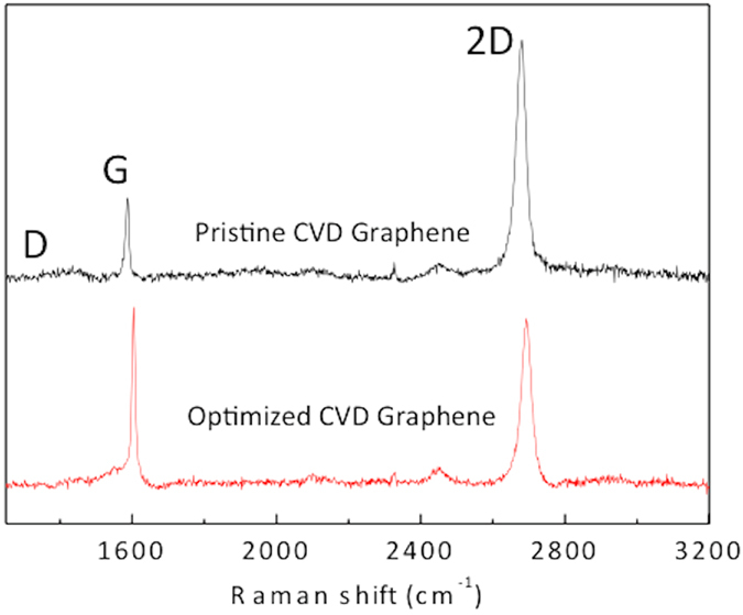
In Fig. 1 we report the Raman spectra of CVD graphene before and after SOCl2 treatment. The hole-doping effect is clearly demonstrated by the red-shift of both the G and 2D peaks and by the increase of the ratio between their intensities17. We note the absence of the D peak in the spectrum of the chemical doped graphene, which attests to the absence of any breaking in the C-sp2 lattice conjugation induced by the SOCl2 treatment. In general, the interaction between SOCl2 and graphitic materials is expected to occur by removing hydroxyl and carboxyl functionalities, and by introducing both covalently and ionically bonded chlorine atoms14,16. Indeed, since the SOCl2/graphene interaction as well as the resulting dopant functionalities on graphene is still the subject of discussion in the literature, the interaction with other SOCl2/graphene reaction products, including SO2, cannot be excluded14.
Figure 1.

Comparison of the Raman spectra of monolayer CVD graphene before (black) and after (red) SOCl2 doping.
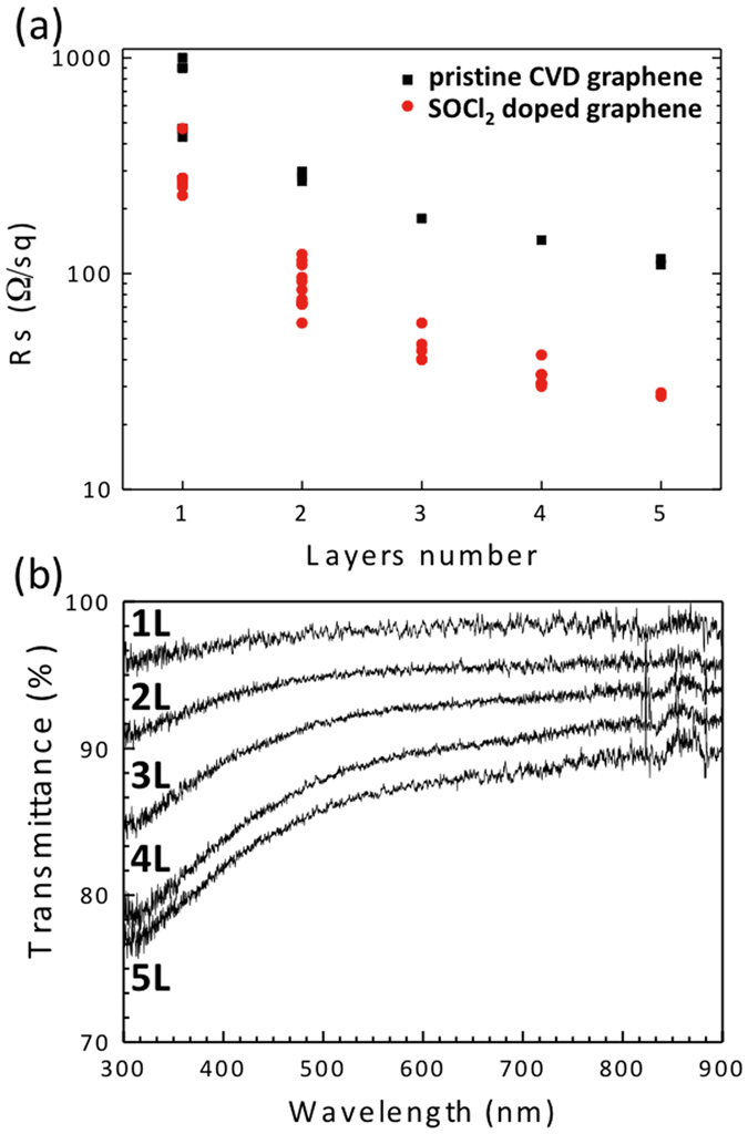
The effect of the combined use of SOCl2 chemical doping and multilayer graphene in terms of sheet resistance is shown in Fig. 2a. In going from the monolayer to five layers the sheet resistance Rs of pristine CVD graphene monotonically decreases and plateaus to values larger than 100 Ω/sq (black solid squares). In contrast, chemically doped graphene can overcome the low threshold limit with only two layers. The minimum sheet resistance value measured for chemically doped graphene is 27 Ω/sq, and was achieved with five-layer graphene samples. If additional graphene layers are added, the effect of series resistances between adjacent graphene layers becomes predominant, resulting in higher Rs.
Figure 2.

(a) Comparison of sheet resistance of 1–5 layers CVD graphene samples on glass substrate with (red circles) and without (black squares) SOCl2 doping. (b) Optical transmittance for 1–5 layer CVD graphene doped by SOCl2 treatment.
The optical transmittance of chemically doped graphene from one to five layers is reported in Fig. 2b. No differences were found between the transmittance values of pristine and chemically doped multilayer graphene. The higher absorbance found for three, four and five graphene layers are related mainly to residual impurities due to the transferal processes, and not to impurities introduced by SOCl2 treatment.
The possibility to operate with very-low sheet resistance samples (quasi-metallic graphene) allowed us to test the electromagnetic response of hole-doped graphene at microwave frequencies. In particular, we measured reflectance, transmittance, and absorbance of samples with different sheet-resistances. The measurements were carried out by means of a microwave setup consisting of a klystron connected to a WR90 rectangular waveguide (the waveguide supports only the TE10 mode). A slotted-line acquired the electromagnetic power (square law) with a spatial resolution of 1 mm in the rectangular waveguide at 9 GHz (the guide wavelength is λg = 48 mm, while the free-space wavelength is λ0 = 33 mm). Further details on the measurement setup are reported in the Supplementary Information (Paragraph SI1).
The analysis is based on the measurement of the standing waves that originate in the rectangular waveguide from the discontinuity at one end of the waveguide. In order to validate the experimental protocol we measured the reflection coefficient Γ when the waveguide is either shorted with a metallic plate or open-ended.
We began our analysis by measuring the response of glass samples covered by graphene sheets with different sheet resistances. The area covered by the doped graphene was about 3 cm × 2 cm, allowing total coverage of the WR90 waveguide cross-section.
We note that the thickness of the hole-doped graphene is of the order of 1 nm, corresponding to ~λ/106, thus confirming the two-dimensional nature of graphene at microwave frequencies.
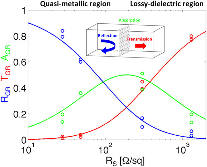
Figure 3 shows experimental reflectance, transmittance and absorbance of the hole-doped graphene when the sheet resistance varies from the lossy-dielectric region to the quasi-metallic range. The solid line refers to the analytical model described and implemented in the Methods (Analytical Model). The comparison between the analytical model and the experimental results shows very good agreement.
Figure 3.

Analytical model (solid line) and experimental findings (circles) for the reflectance RGR (blue), transmittance TGR (red) and absorbance AGR (green) when Rs is varied in the range 10 Ω/sq – 2 kΩ/sq. Please note that the x-axis is in logarithm scale. The maximum absorbance (obtained considering Rs = η0/2 where η0 is the vacuum impedance) separates the quasi-metallic region (Rs < η0/2) from the lossy-dielectric region (Rs > η0/2). The reflectance and transmittance were measured by means of a microwave setup operating at 9 GHz.
We emphasize that the maximum achievable absorption with the doped graphene sheet is equal to 50%, while the graphene in the quasi-metallic region acts as a metal by efficiently reflecting the impinging electromagnetic field. For example, when Rs = 27 Ω/sq the reflectance is larger than 80%. At the same time, the doped graphene sheet conductivity is independent over a wide frequency range (reported theoretically and experimentally in references [6, 7, 8, 9, 10, 11]), which makes the results reported in Fig. 3 also relatively frequency-independent, and may consequently be applied to other regions of the spectrum.
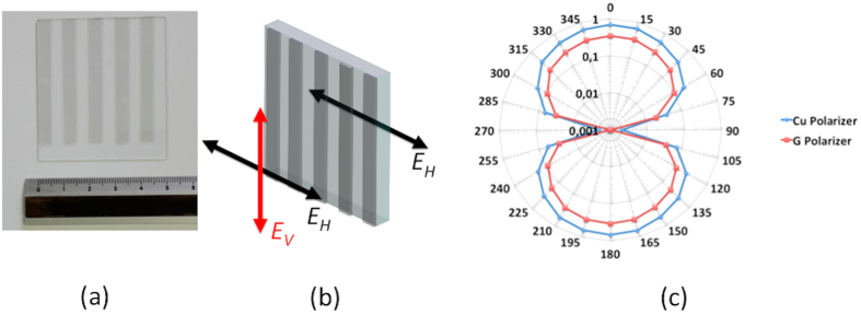
The chemically optimized graphene was exploited to realize a graphene-based wire-grid polarizer, by superimposing four graphene stripes. Using this procedure we achieved a minimum sheet resistance of 50 Ω/sq (quasi-metallic region) in the stripes over an area of about 50 × 55 mm2 (Fig. 4a). The presence of quasi-metallic stripes allows the transmission of the electric field that is polarized along the horizontal direction (EH), while the electric field with vertical polarization (EV) is reflected (Fig. 4b).
Figure 4.
(a) Picture of the fabricated 4-layer-graphene-based wire-grid polarizer; (b) sketch of the graphene-based polarizer and its working principle. (c) Normalized transmittance (T90 – Tpol)/T90 for the graphene-based polarizer (red curve) and the copper-based polarizer (blue curve) where T90 and Tpol are the transmittance at 90° and the polarizer transmittance, respectively.
In order to verify its behavior in terms of polarization, the graphene-based wire-grid polarizer was placed in between two horn pyramidal antennas with a mutual distance larger than that the Fraunhofer distance, thus allowing operation in the far-field (further details are reported in the Supplementary Information). The device was placed on a plastic goniometer (Δ⊖ step was set at 15°) and the transmitted signal was normalized with respect to a reference structure (glass substrate without graphene).
Figure 4 shows the normalized transmittance (T90 – Tpol)/T90 of the polarizer Tpol with respect to transmission at 90° (T90). We adopted this normalization to emphasize the difference at 0° (reflected signal). In fact, the graphene-based wire-grid polarizer (red curve) shows a near-unity transmission at 90°.
We compared the graphene-based wire-grid polarizer with a wire-grid polarizer made with copper stripes of identical dimensions (5 mm width) and identical foot-print with respect to the graphene-based polarizer. The comparison reveals that the two polarizers only show a constant 3 dB difference over the entire angular range while their angular behavior is identical. This result is quite remarkable, considering that the copper layer is 35 μm thick, while graphene thickness is about 1 nm.
Conclusion
In conclusion, we have detailed a chemical protocol for the optimization of graphene in terms of (i) doping stability, (ii) scalability to large areas, and (iii) reduction of the series resistances between graphene layers in multilayer graphene, thus achieving multilayer graphene with sheet resistance values below 30 Ω/sq.
This protocol allowed us to experimentally verify the optimized graphene behavior in terms of reflectance, transmittance, and absorbance of hole-doped graphene when the sheet resistance ranges from that of a lossy-dielectric to that of a quasi-metal.
Finally, the optimized graphene was exploited for the realization of an optically transparent graphene-based polarizer. The comparison between the graphene-based polarizer and its copper-based counterpart revealed that the two polarizers show only a constant 3 dB difference over the entire angular range while their angular behavior remains identical.
The possibility to operate in the quasi-metallic region with very-low sheet resistance graphene may allow the realization of microwave devices (e.g. microstrip patch antennas) and the dynamical tuning of their S-parameters over a wide-range. In this regard, graphene-based antennas with low-sheet resistance graphene may help overcome the limitation of low gain2,3,4.
Methods
CVD graphene growth and transferal
Graphene was grown by CVD on a 25 μm thick copper foils in a typical quartz tube CVD reactor at 1000 °C using CH4/H2 as precursors. The graphene was transferred onto corning glass substrate (treated by O2 plasma to improve graphene adhesion) by the thermal tape method. The copper was etched in a solution of ammonium persulfate. Multilayer graphene samples were fabricated by transferring of additional graphene layers onto graphene/glass substrates.
Chemical doping
SOCl2 treatments were performed in a dry chamber by placing graphene/glass substrate and 1 mL of liquid SOCl2 (avoiding direct contact) at 105 °C for 60 min. Doping of multilayer samples was performed by repeating SOCl2 treatment after transferring and stacking each graphene layer.
Electrical measurements
Sheet resistance measurements were carried out using four-point contacts geometry in the Van der Pauw configuration on a sampled area of 4 × 4 mm2 in air and at room temperature (further details on the measurement setup are reported in the Supplementary Information).
Analytical model
Considering the boundary conditions at the interface z = 0, between two (semi-infinite) media (impinging from medium 1 to medium 2), that introduces a finite sheet conductivity σ2D, we can write:
 |
where η1 and η2 are the wave impedances in the two media, respectively, and  corresponds to Ohm’s law. When graphene is considered in the microwave regime, the graphene sheet conductivity can be approximated by the DC sheet conductivity, i.e. σ2D ≈ σDC = 1/Rs. Moreover, the sheet conductivity is independent over a wide frequency range, as found in references [6, 7, 8, 9, 10, 11]. At the same time, the graphene sheet may be considered as an interface (current sheet) between two media, since its thickness is ~λ/106 at microwave frequencies (X-band). If we apply the boundary conditions for the electric and magnetic fields at the interface z = 0 we obtain:
 |
where Γ and T are the reflection and transmission coefficients, respectively.
Solving the Equation 2 yields to:
 |
where we set  . Reflection and transmission coefficients allow calculation of reflectance RGR and transmittance TGR,
  and
and  , respectively, while absorbance AGR may be evaluated as AGR = 1 – RGR – TGR. If we assume η1 = η2 = η0 (where η0 corresponds to the impedance of free space) it is possible to define two different regions for a single graphene sheet: the lossy-dielectric region
  and the quasi-metallic region
  , where
  defines the sheet resistance that corresponds to the absorbance maximum.
Additional Information
How to cite this article: Grande, M. et al. Optically Transparent Microwave Polarizer Based On Quasi-Metallic Graphene. Sci. Rep. 5, 17083; doi: 10.1038/srep17083 (2015).
Supplementary Material
Acknowledgments
M. Grande thanks the U.S. Army International Technology Center Atlantic for financial support (W911NF-13-1-0434). G.V. Bianco and G. Bruno acknowledge funding from the European Community’s FP7 under grant agreement no. 314578 MEM4WIN and from the National Laboratory Sens&Micro LAB Project (POFESR 2007–2013, code number 15) funded by Apulia Region. This research was performed while the authors M.A. Vincenti and D. de Ceglia held National Research Council Research Associateship awards at the U.S. Army Aviation and Missile Research Development and Engineering Center. A. Sacchetti at CNR-NANOTEC is also acknowledged for his technical assistance during graphene growth and transferring.
Footnotes
Author Contributions M.G., G.V.B., M.A.V., D.d.C., P.C., M.S., A.D.O. and G.B. designed the experiments and discussed the results. M.G. developed the design of the polarizer. G.V.B. and G.B. performed the graphene synthesis, transferring and chemical doping as well as the polarizer fabrication. M.G and G.V.B. carried out the experimental characterization. M.G. and G.V.B. drafted the paper and all authors contributed to the writing.
References
- Kasry A., Kuroda M. A., Martyna G. J., Tulevski G. S. & Bol A. A. Chemical Doping of Large-Area Stacked Graphene Films for Use as Transparent, Conducting Electrodes. ACS Nano 4, 3839–3844 (2010). [DOI] [PubMed] [Google Scholar]
- Dragoman M. et al. A tunable microwave slot antenna based on graphene. Applied Physics Letters 106, 153101 (2015). [Google Scholar]
- Wu B. et al. Microwave absorption and radiation from large-area multilayer CVD graphene. Carbon 77, 814–822 (2014). [Google Scholar]
- Katsounaros A., Cole M. T., Tuncer H. M., Milne W. I. & Hao Y. Near-field characterization of chemical vapor deposition graphene in the microwave regime. Applied Physics Letters 102, 233104 (2013). [Google Scholar]
- Balci O., Polat E. O., Kakenov N. & Kocabas C. Graphene-enabled electrically switchable radar-absorbing surfaces. Nature Communications 6, 6628 (2015). [DOI] [PubMed] [Google Scholar]
- Hanson G. W. Dyadic Green’s functions and guided surface waves for a surface conductivity of graphene. J. Appl. Phys. 103, 064302 (2008). [Google Scholar]
- Hanson G. W. Dyadic Green’s functions for an anisotropic nonlocal model of biased graphene. IEEE Trans. Antennas Propag. 56, 747–757 (2008). [Google Scholar]
- Deligeorgis G. et al. Microwave propagation in graphene. Appl. Phys. Lett. 95, 073107 (2009). [Google Scholar]
- Dragoman M. et al. Coplanar waveguide on graphene in the range 40 MHz–110 GHz. Appl. Phys. Lett. 99, 033112 (2011). [Google Scholar]
- Gomez-Diaz J. S., Perruisseau-Carrier J., Sharma P. & Ionescu A. Non-contact characterization of graphene surface impedance at micro and millimeter waves. J. Appl. Phys. 111, 114908 (2012). [Google Scholar]
- Zhang W., Pham P. H. Q., Brown E. R. & Burke P. J. AC conductivity parameters of graphene derived from THz etalon transmittance, Nanoscale 6, 13895–13899 (2014). [DOI] [PubMed] [Google Scholar]
- Yu Q. et al. Control and characterization of individual grains and grain boundaries in graphene grown by chemical vapour deposition. Nature Materials 10, 443–449 (2011). [DOI] [PubMed] [Google Scholar]
- Li X. et al. Large-Area Graphene Single Crystals Grown by Low-Pressure Chemical Vapor Deposition of Methane on Copper. J. Am. Chem. Soc. 133, 2816 (2011). [DOI] [PubMed] [Google Scholar]
- Wassei J. K., Cha K. C., Tung V. C., Yang Y. & Kaner R. B. The effects of thionyl chloride on the properties of graphene and graphene–carbon nanotube composites, J. Mater. Chem. 21, 3391 (2011). [Google Scholar]
- Eda G. et al. Transparent and conducting electrodes for organic electronics from reduced graphene oxide. Applied Physics Letters 92, 233305 (2008). [Google Scholar]
- Dettlaff-Weglikowska U. et al. Effect of SOCl2 Treatment on Electrical and Mechanical Properties of Single-Wall Carbon Nanotube Networks. J. Am. Chem. Soc. 127, 5125–5131 (2005). [DOI] [PubMed] [Google Scholar]
- Das A. et al. Monitoring dopants by Raman scattering in an electrochemically top-gated graphene transistor. Nature Nanotechnology 3, 210–215 (2008). [DOI] [PubMed] [Google Scholar]
Associated Data
This section collects any data citations, data availability statements, or supplementary materials included in this article.


