

Abstract
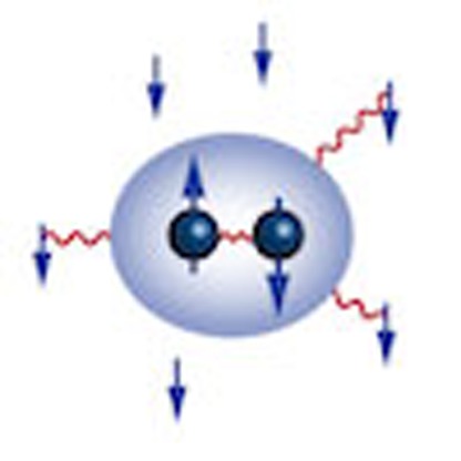
A system of two exchange-coupled Kondo impurities in a magnetic field gives rise to a rich phase space hosting a multitude of correlated phenomena. Magnetic atoms on surfaces probed through scanning tunnelling microscopy provide an excellent platform to investigate coupled impurities, but typical high Kondo temperatures prevent field-dependent studies from being performed, rendering large parts of the phase space inaccessible. We present a study of pairs of Co atoms on insulating Cu2N/Cu(100), which each have a Kondo temperature of only 2.6 K. The pairs are designed to have interaction strengths similar to the Kondo temperature. By applying a sufficiently strong magnetic field, we are able to access a new phase in which the two coupled impurities are simultaneously screened. Comparison of differential conductance spectra taken on the atoms to simulated curves, calculated using a third-order transport model, allows us to independently determine the degree of Kondo screening in each phase.
 Magnetic atoms on a surface possess diverse correlated phases under an applied magnetic field due to a balance of exchange interaction and carrier-mediated coupling. Here, the authors use scanning tunnel microscopy to explore the phase diagram of coupled Co atom pairs on the surface of Cu2N/Cu(100).
The coupling of individual magnetic atoms to the itinerant host electrons of a metal substrate can lead to the formation of a correlated Kondo state in which the magnetic moment is effectively reduced1. This has been shown for 3d-atoms on bare metal surfaces2,3 as well as on thin decoupling layers4,5 and leads to a strong spectroscopic feature at the Fermi energy. Pairs of magnetic atoms are considerably more complex because in addition to the Kondo coupling they can also couple to each other through exchange interactions mediated by the substrate electrons. Depending on their spatial distance, this oscillatory Rudermann–Kittel–Kasuya–Yoshida (RKKY) interaction results in a ferromagnetic (FM) or antiferromagnetic (AFM) coupling6,7,8.
As shown in Fig. 1, the competition between these two effects in combination with an external magnetic field embodies rich physics ranging from a correlated singlet or triplet state to complex Kondo states and has been of considerable theoretical interest for decades9,10,11,12,13,14,15,16. The lower part of this phase space has previously been investigated experimentally through studies at zero magnetic field on coupled quantum dots17, molecules18,19 and atoms on top of20,21,22, as well as buried below23 a metal surface. In particular, controlled mechanical separation of two Kondo atoms enabled continuous tuning between the single impurity Kondo screening and two-impurity singlet phases24. However, field-dependent measurements have so far been hampered by high Kondo temperatures for atoms in direct contact with a metal, resulting in wide resonances that are impossible to split or recombine with experimentally available magnetic fields. Kondo temperatures can be reduced by decoupling the atoms from their host either by means of molecular ligands19,25 or a thin insulating layer4.
Figure 1. Phase diagram of the two-impurity Kondo problem.

Schematic phase diagram of two coupled Kondo-screened spins with varying interaction strength J and external field B transverse to the main anisotropy axis of the individual spins. Kondo screening occurs in the green shaded region. When  is small compared with the characteristic Kondo energy
  , at B=0 the two spins are independently screened by the substrate electrons, while for
 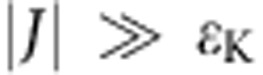 a non-magnetic singlet or high-spin triplet state forms. For J>0 a sufficient B-field can lead to the formation of a new, combined correlated state in which both spins are screened.
Here we use a low-temperature scanning tunnelling microscope (STM) in ultra-high vacuum to assemble pairs of Kondo-screened Co atoms on a thin insulating Cu2N/Cu(100) substrate. By adjusting the relative position and orientation of the atoms on the underlying crystal lattice we are able to tune their exchange interaction strength, and by applying magnetic fields up to 8 T we can access the complete phase space of Fig. 1. Furthermore, by simulating the spectra using a transport model accounting only for weak Kondo coupling, we independently estimate the Kondo screening. We find that when in AFM coupled dimers the field exactly cancels the exchange interaction, Kondo resonances are re-established, signifying a phase transition through the two-impurity Kondo-screened phase.
Results
Spin Hamiltonian
A single Co atom on Cu2N can be described by an effective spin with magnitude S=3/2, and the crystal field induced by the surface is such that the two lowest energy states have magnetization m=±1/2, degenerate in absence of an external magnetic field4. Its differential conductance (dI/dV) spectrum shows a sharp peak at zero excitation voltage, corresponding to a Kondo resonance with a Kondo temperature TK=2.6±0.2 K (ref. 4), equivalent to a characteristic Kondo energy ɛK=kBTK=0.22±0.02 meV, which is much lower than for single atoms directly on2,3 or inside a metal23. This peak splits when a magnetic field is applied due to the Zeeman effect removing the degeneracy of the states with m=±1/2 (ref. 5). If a second magnetic atom is placed adjacent to the first, the Kondo peak splits similarly to when an effective magnetic field is applied; the intensity of this field scales with the strength of the exchange interaction between the two atoms26.
To model the differential conductance spectra we use a single spin anisotropy Hamiltonian in presence of an external magnetic field B, and we assume isotropic Heisenberg exchange J (ref. 27) between the atoms in the dimer:
 |
Here μB is the Bohr magneton and Si refers to the spin on atom i=A, B. The parameters Λμμ (μ=x, y, z) come from second-order expansion of the spin–orbit coupling λL·S (ref. 28) (with spin–orbit constant λ=−21 meV) and represent the extent to which the angular momentum L (which for a free Co atom has magnitude L=3) is unquenched along the μ-direction. Individual Co atoms experience a strong hard-axis anisotropy Λxx=0, Λyy=Λzz=6.4 eV−1 along the vacancy direction (x) of the Cu2N lattice (shown in Fig. 2e), as a result of which the m=±3/2 doublet is split off by 2λ2Λzz=5.6 meV from the lower energy m=±1/2 doublet4. When written in terms of the conventional phenomenological anisotropy parameters D and E (refs 29, 30, 31), this corresponds to D=+2.8 meV, E=0. In most dimers studied here, the intra-dimer exchange coupling J, which can be either AFM (J>0) or FM (J<0), is much weaker than the anisotropy energy 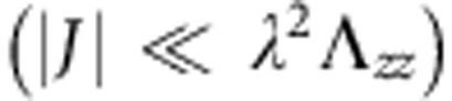 . As a result, each dimer is characterized by a low-energy quartet that consists of combinations of m=±1/2 states of both atoms.
Figure 2. Sign and strength of the exchange interaction between atoms.

(a,b) Energy versus transverse magnetic field of the four lowest energy states for two example dimers, corresponding to the instances presented in panels (c,d) with AFM (J>0) and FM (J<0) coupling respectively. In the AFM case, a state crossing is expected at a field Bc. (c,d) Example of zero-field differential conductance spectra taken on a Co atom in two different dimers. Red and green arrows show, respectively, the exchange and anisotropy energies. In the FM spectrum, an additional step can be resolved at 3/2J. (e) Colour map of the experimentally extracted coupling strength between Co atoms on Cu2N. Each circle corresponds to the position of the second Co atom atop a Cu atom of the lattice, with respect to a reference Co atom (blue sphere). Light grey represent Cu positions too close to allow a Co dimer to be built while the small grey circles are the N atoms. The axes identify the coordinate system for the reference atom, with the nitrogen direction defined as z-axis. (f) Coupling strength versus inter-dimer distance. For comparative purposes, an isotropic three-dimensional RKKY curve with Fermi wavelength of bulk Cu and horizontal offset of 0.15 nm, corresponding to a phase shift of 1.3π, is shown (dashed line). The point represented with an open circle is the {2, 0} dimer, whose coupling cannot be explained in terms of RKKY interaction only. Errors are estimated based on variance found during fitting.
Exchange interaction
For either sign of J, the zero-field energy difference between the lowest and the highest state of the quartet is 4J (Fig. 2a,b). In the limit of J being much smaller than the magnetic anisotropy, the energy difference between the ground state and the first excited state is ∼(5/2)J or ∼(3/2)J for AFM or FM coupling, respectively. Figure 2c,d show two dI/dV spectra taken on Co atoms in two different dimers, where each step-like increase in the differential conductance corresponds to a spin excitation from the ground state to an excited state, and in which the two energy scales 4J and 2λ2Λzz are clearly distinguishable. The evolution of the energetically lowest excitation as a function of magnetic field (in our experiment applied along the transverse direction y) reveals the sign of J. For AFM coupling, the step-energy decreases until the critical field Bc=(13/8) × J/(gμB) is reached, (g=2−2λΛyy), at which the ground state and the first excited state become degenerate (Fig. 2a). At B>Bc these states change their order and their energy difference increases with field. For FM coupling, the step-energy will only increase with increasing field and a crossing between the ground state and the first excited state does not occur (Fig. 2b).
Following these considerations, we can extract the coupling value between any two atoms placed on the Cu2N surface through differential conductance spectroscopy. In Fig. 2e we show the obtained coupling map with respect to a reference Co atom drawn in the centre. Depending on the relative distance and orientation between the atoms in the pair that can be placed only in specific positions allowed by the substrate, the coupling can be tuned in strength and sign. The obtained results are in good agreement with the coupling values that were previously extracted for Fe dimers32.
In previous experiments33 and theoretical calculations14,34 on magnetic atoms directly on a metal surface, the dominant exchange mechanism was found to be RKKY interaction6,7,8. It is not known to what extent this is still true in the current case, where the adatoms are embedded in a covalently bonded network29 which decouples them from the substrate conduction electrons mediating this interaction. In Fig. 2f we plot the extracted coupling value of each dimer as a function of the absolute separation distance. We classify each dimer by the number of unit cells separating the Co atoms in the two symmetry directions of the underlying Cu2N lattice, first stating the distance along the nitrogen direction (z) and then along the vacancy direction (x): {N, v}. For all dimers studied except the {2, 0} type depicted with a different symbol, the coupling dependence on the distance seems to be qualitatively comparable to isotropic bulk RKKY (ref. 35), shown in the same figure for comparative purposes only. A full theoretical treatment of the RKKY coupling on this composite surface, in which also anisotropic RKKY interaction36 could play a role, is beyond the scope of this paper.
In the case of the {2, 0} dimer, the exchange coupling is an order of magnitude larger than for the equally spaced {0, 2} dimer. According to isotropic RKKY theory the coupling strength and sign depend only on absolute distance, and should therefore be identical for these two dimers. In this particular case we believe that, in addition to RKKY interaction, superexchange coupling plays an important role37. Being mediated by the Co–N and Cu–N bonds separating the two Co atoms, superexchange coupling should be strongly direction-dependent: every 90° corner in the coupling path significantly reduces its magnitude38,39. Of all dimers studied, the {2, 0} geometry is the only case where the two Co atoms are connected by a series of bonds without any corner. To further investigate the role of superexchange interaction, dimers would have to be built in which Co atoms are separated by a single N atom only, which so far we have not been able to do controllably.
Spectroscopy measurements
We measured dI/dV spectra on every atom of each dimer at different values of external magnetic field applied perpendicular to the sample plane, transverse to the magnetic hard-axis (Fig. 3b–f). For comparison, spectra taken on a single Co are shown in Fig. 3a. In addition, we simulate the experimental data by diagonalizing the Hamiltonian (1) and using a perturbative scattering model in which the tunnelling electrons interact with the localized spin S via an exchange interaction S·σ, with σ=(σx, σy, σz) the standard Pauli matrices for spin-1/2 electrons40. In the differential conductance curves of Fig. 3b–e, the magnetic anisotropy is best described with Λxx=0, and Λyy and Λzz varying between 6.1 and 7.0 eV−1, very close to the single Co values. However, this is not the case for the {2, 0} dimer, presented in Fig. 3f, for which Λzz=2Λyy. We believe that in this structure the strain induced by the presence of the second atom is playing a critical role, enhancing the magnetic anisotropy32,41 (Supplementary Fig. 1 and Supplementary Note 1).
Figure 3. Overview of dimer configurations: experimental data and simulated spectra.

(a–f) Measured dI/dV spectra (blue dots) and simulated curves (green lines) on a single Co atom and on all five types of dimers showing a measurable coupling, presented with increasing value of 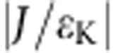 , with ɛK=0.22±0.02 meV, for zero magnetic field and fields applied in the y direction, perpendicular to the sample surface. Orange shaded regions mark the difference between measurement and simulation in the voltage range from −3 to +3 mV. Field spectra have been offset for clarity; all measurements were performed at 330 mK. A corresponding atomic lattice diagram and topographic STM image (scale bar, 1 nm) are shown for each type of dimer. Large and small grey circles represent, respectively, Cu and N atoms; the blue spheres the Co atoms. The arrows in panels b and d indicate which atom of the dimer is presented in the figure; those are the only two cases in which the two atoms are not equivalent. (g) MSE between the data and the simulated conductance curve as a function of J/ɛK for zero field (blue), 4 T (green) and 8 T (red).
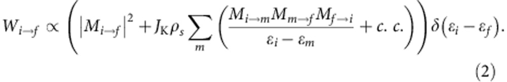
We account for scattering up to third order in the matrix elements by additionally considering an AFM spin–spin Kondo-exchange coupling JKρs between the substrate electrons and the localized spin system42,43, with ρs the density of states in the substrate around the Fermi energy. When the exchange interaction J between the Co spins is large compared with the Kondo energy ɛK, that is, 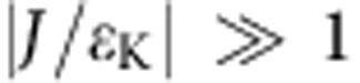 , we find very good agreement between model and experimental data when using a constant exchange coupling of JKρs=0.15. This value is in accordance with previous results44,45,46. Additional parameter values are listed in Supplementary Table 1.
This model cannot account for the additional spectral weight which arises when the localized spin system enters a state in which it is strongly screened by the substrate electrons. For example, the zero-field Kondo peak of a single Co atom (Fig. 3a) is strongly underestimated in the simulations. The observed discrepancy arises most likely from the fact that the model accounts only for correlations induced by scattering events up to third order during the tunnelling process, meaning that processes involving interaction with more than a single substrate electron are not taken into account43. In a full theoretical treatment of the Kondo interaction, higher order scattering between the localized spin and the substrate electrons produces correlations which strongly influences the spectral weight around the Fermi energy, leading to an increased tunnelling probability and therefore a higher conductance at zero bias.
The difference between measured and simulated spectra provides an easily accessible quantitative measure for the degree of Kondo screening in the system. In Fig. 3g we have plotted the mean square error (MSE), defined as 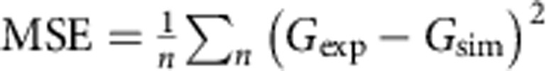 (with n the number of data points in the voltage range and Gexp and Gsim, respectively, the normalized measured and simulated conductance), as a function of J/ɛK. The MSE, which was determined for spectra at zero field, 4 and 8 T in the voltage range from −3 to 3 mV, scales with the areas coloured in yellow in Fig. 3a–f (Fig. 3g). We find that for larger field values, the region of largest MSE shifts in the direction of positive J/ɛK, as expected based on the phase diagram in Fig. 1.
Intriguingly, in the case of AFM coupling, the combined ground state at zero field is the non-magnetic singlet which we can deliberately tune to different phases by applying an external magnetic field. The field effectively counteracts the exchange interaction leading to a crossing of the singlet state with the lowest triplet state at the critical field Bc. Around this degeneracy point, the system enters a new phase in which the two impurities are together Kondo-screened by the substrate electrons (Fig. 1). Among the dimers studied, there are three with AFM coupling. For the {2, 0} dimer the coupling is so strong that the state crossing occurs at a field much larger than 9 T, not accessible in our experimental set-up. For the other two cases, {0, 2} and {3/2, 1/2}, the crossings are at ∼3 and ∼5 T, respectively.
In Fig. 4a,b we show a series of dI/dV spectra measured around these crossing points for the two dimers in the voltage range from −3 to 3 mV. Here, we clearly observe the emergence of Kondo screening concomitant with a zero-voltage peak in the dI/dV spectrum, which disappears quickly at fields larger or smaller than Bc. Note that this two-impurity Kondo state differs significantly from that of a single atom at zero field (Fig. 3a): it reflects the combined screening of the dimer by the substrate electrons. In addition to the central Kondo peak the spectra show low-energy features near the crossing. These features, that cannot be captured by our current model, may contain additional information about the two-impurity Kondo screening phase. Due to some of these features being close to the central peak, it is difficult to extract the exact Kondo line width. However, in both cases the Kondo peak is clearly wider than the thermal energy of our measurement, which is ∼30 μeV.
Figure 4. Two-impurity Kondo screening phase.

(a,b) Differential conductance spectra for the {0, 2} and the {3/2, 1/2} dimer, respectively, around the critical field of each pair. (c) Phase diagram of the two-impurity Kondo problem showing the locations of performed measurements; white markers refer to panels a,b. The data points marked with a square indicate the presence of a Kondo resonance. The solid line marks the position of the ground state degeneracy.
Figure 4c shows the locations of all presented measurements in the phase diagram of Fig. 1. All possible phases are found in our data. The FM {1, 1} dimer is always in the two-impurity triplet state, while the AFM {2, 0} dimer is always a two-impurity singlet; for those two instances, no Kondo screening is observed. The weakly FM-coupled {3/2, 3/2} dimer is very similar to the single Co: at zero field it behaves like a single Kondo-screened impurity, whereas for large fields the two atoms are separate paramagnetic moments. Lastly, the {0, 2} and the {3/2, 1/2} both undergo a phase transition from the singlet-phase to being separate moments through the two-impurity Kondo screening phase.
Discussion
In summary, we have been able to experimentally explore the complete phase space of a system of two coupled Kondo atoms in a magnetic field. We showed that for AFM coupled dimers the phase can be continuously tuned from the two-impurity singlet to the single impurity local moment phase solely by an external magnetic field, leading to the formation of the correlated two-impurity Kondo screening phase at the critical crossover field. This transition, which is fundamentally different from the previously investigated zero-field transition between the single impurity Kondo screening and two-impurity singlet phases24, technically constitutes a quantum phase transition, even though our experiments do not allow us to reveal the associated quantum critical behaviour12. Using a third-order perturbative transport model, we have demonstrated that the spectra can be well reproduced except in the vicinity of the ground state crossings, where additional weight around zero bias voltage occurs. These results may form the basis for future work on one and two-dimensional engineered Kondo lattices.
Methods
Experimental set-up
The experiments were performed in a commercial STM system (Unisoku USM 1300 S), at low-temperature (330 mK) and in ultra-high vacuum (<2 × 10⁻¹⁰ mbar). Magnetic fields up to 8 T were applied perpendicular to the sample surface and the hard uniaxial anisotropy of the Co atoms. The Cu2N/Cu(100) sample was prepared in situ by N2 sputtering on the clean Cu crystal47; Co atoms were evaporated on the precooled Cu2N. The STM tip, made of PtIr, was prepared by indentation in the bare Cu surface. Co dimers were built via vertical atom manipulation48. dI/dV spectra were recorded with a non-polarized tip, using a lock-in technique with excitation voltage amplitude of 70–100 μVRMS at 928 Hz. The tunnel current for spectroscopy was set between 1.5 and 2 nA at −10 or −15 mV sample bias for different types of dimer. Variation of the distance between the tip and the atoms up to 150 pm (corresponding to a factor ∼30 variation in tunnel current) on the same atom did not lead to any significant modification of the spectral lineshapes. The resolution of the spectral features is limited mostly by the temperature and the lock-in modulation.
Simulations
The simulation of the differential conductance curves was performed using a perturbative approach established by Appelbaum, Anderson, and Kondo49,50,51,52, which accounts for spin-flip scattering processes up to third order in the matrix elements. The transition probability Wi→f for an electron to tunnel between tip and sample or vice versa and simultaneously changing the quantum state of the dimer system between the initial (i) and final (f) state is in this model given by:
 |
In this expression,  is the scattering matrix element from the combined state vector
 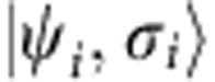 to
to  , with
  as the eigenstate of the localized spin system and σ as the wavevector of the interacting electron. Energy conservation between initial energy ɛi and final energy ɛf is obeyed by the delta distribution δ(ɛi−ɛf) in equation (2).
The first term of equation (2) is responsible for the conductance steps observed in the spectra29, while the second term leads to logarithmic peaks at the intermediate energy ɛm and scales with the coupling JKρs to the substrate42. Note, that this model cannot cover strong correlations because it neglects higher order effects.
Additional information
How to cite this article: Spinelli, A. et al. Exploring the phase diagram of the two-impurity Kondo problem. Nat. Commun. 6:10046 doi: 10.1038/ncomms10046 (2015).
Supplementary Material
Supplementary Figure 1, Supplementary Table 1, Supplementary Note 1 and Supplementary References.
Acknowledgments
This work was supported by the Dutch Organizations FOM and NWO (VIDI) and by the Kavli Foundation. M.T. acknowledges support by the SFB 767.
Footnotes
Author contributions A.S., M.G., R.T. and B.B. performed the experiments and analysed the data. A.S, M.T. and A.F.O. wrote the manuscript. All authors discussed the results and commented on the manuscript.
References
- Hewson A. C. The Kondo Problem to Heavy Fermions Cambridge University Press (1997). [Google Scholar]
- Madhavan V., Chen W., Jamneala T., Crommie M. F. & Wingreen N. S. Tunneling into a single magnetic atom: spectroscopic evidence of the Kondo resonance. Science 280, 567–569 (1998). [DOI] [PubMed] [Google Scholar]
- Li J., Schneider W.-D., Berndt R. & Delley B. Kondo scattering observed at a single magnetic impurity. Phys. Rev. Lett. 80, 2893–2896 (1998). [Google Scholar]
- Otte A. F. et al. The role of magnetic anisotropy in the Kondo effect. Nat. Phys. 4, 847–850 (2008). [Google Scholar]
- von Bergmann K., Ternes M., Loth S., Lutz C. P. & Heinrich A. J. Spin polarization of the split Kondo state. Phys. Rev. Lett. 114, 076601 (2015). [DOI] [PubMed] [Google Scholar]
- Ruderman M. A. & Kittel C. Indirect exchange coupling of nuclear magnetic moments by conduction electrons. Phys. Rev. 96, 99–102 (1954). [Google Scholar]
- Kasuya T. A theory of metallic ferro- and antiferromagnetism on Zener's model. Prog. Theor. Phys. 16, 45–57 (1956). [Google Scholar]
- Yosida K. Magnetic properties of Cu-Mn alloys. Phys. Rev. 106, 893–898 (1957). [Google Scholar]
- Jayaprakash C., Krishna-Murthy H. R. & Wilkins J. W. Two-impurity Kondo problem. Phys. Rev. Lett. 47, 737–740 (1981). [Google Scholar]
- Jones B. A. & Varma C. M. Study of two magnetic impurities in a Fermi gas. Phys. Rev. Lett. 58, 843–846 (1987). [DOI] [PubMed] [Google Scholar]
- Jones B. A., Varma C. M. & Wilkins J. W. Low-temperature properties of the two-impurity Kondo Hamiltonian. Phys. Rev. Lett. 61, 125–128 (1988). [DOI] [PubMed] [Google Scholar]
- Jones B. A. & Varma C. M. Critical point in the solution of the two magnetic impurity problem. Phys. Rev. B 40, 324–329 (1989). [DOI] [PubMed] [Google Scholar]
- Silva J. B. et al. Particle-hole asymmetry in the two-impurity Kondo model. Phys. Rev. Lett. 76, 275–278 (1996). [DOI] [PubMed] [Google Scholar]
- Simon P., Lopez R. & Oreg Y. Ruderman-Kittel-Kasuya-Yosida and magnetic-field interactions in coupled Kondo quantum dots. Phys. Rev. Lett. 94, 086602 (2005). [DOI] [PubMed] [Google Scholar]
- Žitko R. Kondo screening in high-spin side-coupled two-impurity clusters. J. Phys. Condens. Matter 22, 026002 (2010). [DOI] [PubMed] [Google Scholar]
- Jabben T., Grewe N. & Schmitt S. Spectral properties of the two-impurity Anderson model with varying distance and various interactions. Phys. Rev. B 85, 045133 (2012). [Google Scholar]
- Craig N. J. et al. Tunable nonlocal spin control in a coupled-quantum dot system. Science 304, 565–567 (2004). [DOI] [PubMed] [Google Scholar]
- Wegner D. et al. Tuning molecule-mediated spin coupling in bottom-up-fabricated vanadium-tetracyanoethylene nanostructures. Phys. Rev. Lett. 103, 087205 (2009). [DOI] [PubMed] [Google Scholar]
- Tsukahara N. et al. Evolution of Kondo resonance from a single impurity molecule to the two-dimensional lattice. Phys. Rev. Lett. 106, 187201 (2011). [DOI] [PubMed] [Google Scholar]
- Jamneala T., Madhavan V. & Crommie M. F. Kondo response of a single antiferromagnetic chromium trimer. Phys. Rev. Lett. 87, 256804 (2001). [DOI] [PubMed] [Google Scholar]
- Wahl P. et al. Exchange interaction between single magnetic adatoms. Phys. Rev. Lett. 98, 056601 (2007). [DOI] [PubMed] [Google Scholar]
- Néel N. et al. Two-site Kondo effect in atomic chains. Phys. Rev. Lett. 107, 106804 (2011). [DOI] [PubMed] [Google Scholar]
- Prüser H. et al. Interplay between the Kondo effect and the Ruderman-Kittel-Kasuya-Yosida interaction. Nat. Commun. 5, 5417 (2014). [DOI] [PubMed] [Google Scholar]
- Bork J. et al. A tunable two-impurity Kondo system in an atomic point contact. Nat. Phys. 7, 901–906 (2011). [Google Scholar]
- Dubout Q. et al. Controlling the spin of Co atoms on Pt(111) by hydrogen adsorption. Phys. Rev. Lett. 114, 106807 (2015). [DOI] [PubMed] [Google Scholar]
- Otte A. F. et al. Spin excitations of a Kondo-screened atom coupled to a second magnetic atom. Phys. Rev. Lett. 103, 107203 (2009). [DOI] [PubMed] [Google Scholar]
- Fernández-Rossier J. Theory of single-spin inelastic tunneling spectroscopy. Phys. Rev. Lett. 102, 256802 (2009). [DOI] [PubMed] [Google Scholar]
- Dai D., Xiang H. & Whangbo M. H. Effects of spin-orbit coupling on magnetic properties of discrete and extended magnetic systems. J. Comput. Chem. 29, 2187–2209 (2008). [DOI] [PubMed] [Google Scholar]
- Hirjibehedin C. F. et al. Large magnetic anisotropy of a single atomic spin embedded in a surface molecular network. Science 317, 1199–1203 (2007). [DOI] [PubMed] [Google Scholar]
- Brune H. & Gambardella P. Magnetism of individual atoms adsorbed on surfaces. Surf. Sci. 603, 1812–1830 (2009). [Google Scholar]
- Gatteschi D., Sessoli R. & Villain J. Molecular Nanomagnets Oxford University Press (2006). [Google Scholar]
- Bryant B., Spinelli A., Wagenaar J. J. T., Gerrits M. & Otte A. F. Local control of single atom magnetocrystalline anisotropy. Phys. Rev. Lett. 111, 127203 (2013). [DOI] [PubMed] [Google Scholar]
- Khajetoorians A. A. et al. Atom-by-atom engineering and magnetometry of tailored nanomagnets. Nat. Phys. 8, 497–503 (2012). [Google Scholar]
- Simon E. et al. Exchange interaction between magnetic adatoms on surfaces of noble metals. Phys. Rev. B 83, 224416 (2011). [Google Scholar]
- Kittel C. Quantum Theory of Solids Wiley (1987). [Google Scholar]
- Zhou L. et al. Strength and directionality of surface Ruderman-Kittel-Kasuya-Yosida interaction mapped on the atomic scale. Nat. Phys. 6, 187–191 (2010). [Google Scholar]
- Pavarini E., Koch E., Anders F. & Jarrel M. Correlated Electrons: From Models to Materials. Modeling and Simulation Vol. 2, Forschungszentrum Jüilich (2012). [Google Scholar]
- Goodenough J. B. An interpretation of the magnetic properties of the peroskite-type mixed crystals La1−xSrxCoO3−λ. J. Phys. Chem. Solids 6, 287–297 (1958). [Google Scholar]
- Kanamori J. Superexchange interaction and symmetry properties of electron orbitals. J. Phys. Chem. Solids 10, 87–98 (1959). [Google Scholar]
- Loth S. et al. Controlling the state of quantum spins with electric currents. Nat. Phys. 6, 340–344 (2010). [Google Scholar]
- Bryant B. et al. Controlled complete suppression of single-atom inelastic spin and orbital cotunnelling. Nano Lett. 15, 6542–6546 (2015). [DOI] [PubMed] [Google Scholar]
- Zhang Y.-H. et al. Temperature and magnetic field dependence of a Kondo system in the weak coupling regime. Nat. Commun. 4, 2110 (2013). [DOI] [PMC free article] [PubMed] [Google Scholar]
- Ternes M. Spin excitations and correlations in scanning tunneling spectroscopy. New. J. Phys. 17, 063016 (2015). [Google Scholar]
- Delgado F., Hirjibehedin C. F. & Fernández-Rossier J. Consequences of Kondo exchange on quantum spins. Surf. Sci. 630, 337–342 (2014). [Google Scholar]
- Spinelli A., Bryant B., Delgado F., Fernandez-Rossier J. & Otte A. F. Imaging of spin waves in atomically designed nanomagnets. Nat. Mater. 13, 782–785 (2014). [DOI] [PubMed] [Google Scholar]
- Oberg J. C. et al. Control of single-spin magnetic anisotropy by exchange coupling. Nat. Nanotechnol 9, 64–68 (2014). [DOI] [PubMed] [Google Scholar]
- Leibsle F. M., Flipse C. F. J. & Robinson A. W. Structure of the Cu{100}-c(2 × 2)N surface: a scanning-tunneling-microscopy study. Phys. Rev. B 47, 15865–15868 (1993). [DOI] [PubMed] [Google Scholar]
- Hirjibehedin C. F., Lutz C. P. & Heinrich A. J. Spin coupling in engineered atomic structures. Science 312, 1021–1024 (2006). [DOI] [PubMed] [Google Scholar]
- Kondo J. Resistance minimum in dilute magnetic alloys. Prog. Theor. Phys. 32, 37–49 (1964). [Google Scholar]
- Appelbaum J. A. ‘s-d' Exchange model of zero-bias tunneling anomalies. Phys. Rev. Lett. 17, 91–95 (1966). [Google Scholar]
- Anderson P. W. Localized magnetic states and Fermi-surface anomalies in tunneling. Phys. Rev. Lett. 17, 95–97 (1966). [Google Scholar]
- Appelbaum J. A. Exchange model of zero-bias tunneling anomalies. Phys. Rev. 154, 633–643 (1967). [Google Scholar]
Associated Data
This section collects any data citations, data availability statements, or supplementary materials included in this article.
Supplementary Materials
Supplementary Figure 1, Supplementary Table 1, Supplementary Note 1 and Supplementary References.