

Abstract
High-pressure high-temperature (HPHT) nanodiamonds originate from grinding of diamond microcrystals obtained by HPHT synthesis. Here we report on a simple two-step approach to obtain as small as 1.1 nm HPHT nanodiamonds of excellent purity and crystallinity, which are among the smallest artificially prepared nanodiamonds ever shown and characterized. Moreover we provide experimental evidence of diamond stability down to 1 nm. Controlled annealing at 450 °C in air leads to efficient purification from the nondiamond carbon (shells and dots), as evidenced by X-ray photoelectron spectroscopy, Raman spectroscopy, photoluminescence spectroscopy, and scanning transmission electron microscopy. Annealing at 500 °C promotes, besides of purification, also size reduction of nanodiamonds down to ∼1 nm. Comparably short (1 h) centrifugation of the nanodiamonds aqueous colloidal solution ensures separation of the sub-10 nm fraction. Calculations show that an asymmetry of Raman diamond peak of sub-10 nm HPHT nanodiamonds can be well explained by modified phonon confinement model when the actual particle size distribution is taken into account. In contrast, larger Raman peak asymmetry commonly observed in Raman spectra of detonation nanodiamonds is mainly attributed to defects rather than to the phonon confinement. Thus, the obtained characteristics reflect high material quality including nanoscale effects in sub-10 nm HPHT nanodiamonds prepared by the presented method.
Introduction
Nanodiamonds (NDs) belong to a family of carbon-based nanomaterials1 that are promising for numerous applications. Applications of NDs in biology such as imaging,2,3 drug delivery, or gene therapy4 as well as in spintronic5 and photonic6 are the most topical. Because the ratio of surface atoms on typical 5 nm ND is already ∼15%, the structure and chemistry of the surface determines the ND properties to a great extent. For instance, surface termination was shown to control photoluminescence (PL) of NDs from NV centers via electric dipoles of the surface atoms.7,8 High-quality surface oxidation9,10 or fluorination11 leads to enhancement of NV– over NV0 color centers population, while surface-states-related broad band PL is efficiently quenched at the same time. Thus, an attention is increasingly focused on the well-defined surface chemistry and purity of NDs, in particular, for their biological or electronic applications.12
There are various sources of NDs. When sub-10 nm NDs are required the DND13 (detonation nanodiamond) is the typical choice at present. They have the characteristic, narrow size distribution of 5 ± 2 nm, although considerable decrease in their mean size down to 2.8 nm using nanosized explosives was recently reported.14,15 On the contrary, separation of individual DNDs is not a straightforward process due to a complex, hierarchical structure of the detonation soot they have to be isolated from.16 In addition, a DND nanoparticle itself exhibits a complex structure given by its detonation origin. A DND nanoparticle is often modeled by a diamond core, including various lattice defects, transient sp3/sp2 layer, and sp2 surface shell that may carry various surface functional groups.17 Lattice defects in DNDs can inactivate laboriously created color centers by acting as sink (low energy) sites. NDs with well-defined inner structure and surface in the DND size range are currently missing.
One of the candidates may be NDs, which arise from mechanical grinding of high-quality HPHT (high-pressure high-temperature) diamond microcrystals. Their main advantage over DNDs is the expected uniform structure with low concentration of lattice defects such as dislocations or twinning. This is particularly important for their spintronic and sensing applications as they may stably host various color centers.18−20 Ultrasmall HPHT NDs receive a growing attention21,22 as the size of HPHT NDs below 10 nm may facilitate easier cell penetration, which together with the shape, their aggregation stage, and their surface charge play important role.23 NDs smaller than 10 nm may thus enable efficient molecular tracking biological applications as well as general exploration of nanoscale-related phenomena in high-quality diamond. The finest HPHT NDs available nowadays on the market have a size median of ∼18 nm. Similar HPHT diamond powder (median size of 25 nm) was recently reported to contain 60% of sub-10 nm particles, as revealed by a transmission electron microscopy (TEM) analysis.24 The particle size thus approaches that of DNDs, although their size distribution is broader due to the grinding processes they arise from. Another study showed that an acceleration of 8.65 × 10⁴g for 40 min in a centrifuge can provide NDs with median size of 4 nm starting from a HPHT material with median size of 30 nm;25 however, in both cases, no attention was paid to material characterization of the separated sub-10 nm NDs.
Yet raw ND powders (i.e., detonation or HPHT) are well-known to contain also nondiamond carbon, metal, and metal oxides impurities coming either from the grinding process in the case of HPHT NDs or from the explosive chamber and explosion event itself in the case of DNDs. Many manufacturers use wet chemical post-treatments to address the purity and surface chemistry of the NDs such as H2SO4, mixture of H2SO4/HNO3, HCl, and K2CrO4 in H2SO4 for removing metallic impurities and KOH/KNO3, Na2O2, CrO3/H2SO4, and HNO3/H2O2 under pressure for nondiamond carbon etching. Numerous other purification approaches have been reviewed by Schrand et al.4 Oxidation in air26−28 at elevated temperatures and oxidation in ozone29,30 have been demonstrated as alternative and effective approaches for nondiamond carbon phase removal and surface oxidation of NDs. In particular the air-oxidized NDs were shown to be chemically stable in ambient air despite their nanoscale dimensions.31
In this study we describe an efficient approach how to obtain sub-10 nm HPHT NDs down to 1 nm with excellent purity and crystallinity by optimized control of annealing time and temperature in air, followed by a relatively short centrifugation step. We present comprehensive microscopic, scattering, thermogravimetric, photoelectron, Raman, infrared, and photoluminescence analysis and provide structural, chemical and photoluminescence correlations. We show that it is possible to prepare and separate sub-10 nm HPHT NDs with a distribution function close to the DNDs but with considerably better structural quality. At the same time, a considerable fraction of probably smallest man-made NDs as small as 1.1 nm is obtained and visualized by scanning transmission electron microscopy (STEM). This demonstrates the stability of diamond down to 1 nm. By means of particularly Raman spectroscopy, we demonstrate a real phonon confinement effect in sub-10 nm NDs.
Materials and Methods
Nanodiamonds Preparation
Monocrystalline synthetic NDs of HPHT origin with a median size of 18 nm (MSY 18, size range: 0–25 nm) were purchased from Microdiamant AG. The NDs were used as received or annealed in air at 450 °C for 30, 60, and 120 min and at 500 °C for 30 min. Deionized water-based colloidal solutions with concentration of 20 mg/mL were prepared from the as-received and annealed MSY 18 HPHT NDs. The solutions were ultrasonicated by means of an ultrasound horn (Hielscher) at 200 W for 1 h to ensure a proper dispersion and then centrifuged (Eppendorf Mini plus) at 14 000 rpm (13 124g) for 1 h. 1 mL of supernatant was carefully separated by a micropipette to isolate the smallest NDs. This resulted in the set of five samples: MSY18-asrec (as-received NDs), MSY18-O1 (annealed 30 min, 450 °C), MSY18-O2 (annealed 60 min, 450 °C), MSY18-O3 (annealed 120 min, 450 °C), and MSY18-O4 (annealed 30 min, 500 °C).
We further involved commercial DNDs (distributor: New Metals and Chemicals, Kyobashi, manufacturer: Lingyun Granda Nano (China)) with nominal size of 5 nm as a reference. These DNDs are made from TNT (trinitrotoluene) and RDX (hexogen) charge, cooled by surrounding water shell. Colloidal solutions were obtained from these DNDs by the same approach as previously described, that is, after ultrasonic treatment and centrifugation. Two particular colloidal samples were prepared: DND-asrec (as-received DNDs) and DND-O (air-annealed 30 min, 450 °C).
Characterizations
For atomic force microscopy (AFM) analysis, Si substrates (p-type, 3–8 Ωcm, MEMC Electronic Materials) covered by a native oxide layer were immersed in the NDs colloidal solutions and placed in an ultrasonic bath for 30 min to achieve a moderate coverage. AFM images were acquired by NTegra Prima (NT-MDT) using PPP NCSTR Si tips (Nanosensors) in a noncontact regime. To obtain particle size histograms from the AFM topography data, we performed the particle analysis procedure on at least three randomly chosen spots on the sample. The sizes of the particles were determined from a maximum height of a particle values to exclude the effect of the tip convolution. The particle size analysis was performed by the AFM software from the 256 × 265 images. Because the image size was 1 × 1 μm2, the length of the scanner step was 3.9 nm laterally. Because a typical 3 nm particle was imaged having diameter of ∼20 nm, ∼5 pixels (x, y, z coordinates) were recorded on such particle, which provide reasonable accuracy. At the same time, the tip was still sharp enough to distinguish the vast majority of single particles. A minimum number of nanoparticles used for the particle size determination was always >1000. Particles were assumed to be perfect spheres to extract the volume fraction. Although the particles located on the image borders were not excluded from the analysis, it did not have any significant effect on the obtained size distribution.
Dynamic light scattering (DLS) measurements of colloidal solutions were performed on a Malvern instrument Zetasizer Nano ZS equipped with a helium–neon laser (633 nm); the scattering angle was 173°. The refractive index of bulk diamond (2.4) was used to convert the measured intensity/size distributions to volume/size distributions as the Rayleigh approximation predicts that the intensity of the light scattered is proportional to particle diameter by r6, and so even small concentration of larger particles would dominate the intensity spectrum.
The thermogravimetric analysis (TGA) was done using a homemade apparatus constructed of a computer-controlled oven and a Sartorius BP210 S balance. The measurements were carried out in air between 30 and 960 °C at a heating rate of 5 °C min–1. For TGA analysis, raw MSY18 and DND powders were used in an as-received state.
X-ray powder diffraction using Bruker D8 diffractometer (CuKa radiation) was employed to determine the lattice parameters and crystallite sizes of NDs. X-ray diffraction patterns were analyzed with the Rietveld method using the FULLPROF program.
A TEM grid covered with CVD-grown graphene (purchased from Graphenea) was dipped into colloidal solution of NDs and then rinsed in isopropanol. To avoid damage of the graphene support caused by surface tension during drying, a critical point drying technique was used. STEM imaging was carried out with a Nion UltraSTEM 100 operated at 60 kV in ultrahigh vacuum. The achieved structural resolution was 1 Å.
Material quality of NDs was characterized by micro-Raman spectroscopy. Raman spectra were measured by using a Renishaw InVia Raman microspectrometer with UV excitation wavelength of 325 nm. The intensity of the incident laser was below 1 mW to minimize possible heat-induced changes of the samples. A volume of 20 μL of the colloidal solution was applied on a Si substrate by drop-casting and dried at 100 °C for 2 min to evaporate the water. All measurements were performed with a 40× objective with numerical aperture 0.5, resulting in the laser spot diameter of 20 μm. The accumulation time was set to 100 s to increase the signal-to-noise ratio. A spectral calibration was done on a bulk monocrystalline diamond sample.
Photoluminescence of NDs in the form of colloidal solutions was excited by the third harmonic (355 nm) of pulsed Nd:YAG laser (8 ns long pulses, 10 Hz repetition rate, and excitation power density of 100 kW/cm2). The photoluminescence signal was collected with an optical fiber coupled to a spectrograph Shamrock with gated intensified CCD camera Andor (minimal gate width of 4 ns, irising effect of 0.2 ns).32 The integrated spectra were measured within the detection gate of 100 ns. The time-resolved spectra were measured by shifting the 5 ns long detection gate by steps of 1 ns. The detection gate was pretriggered to detect also the rise of the signal. The measured spectra were corrected for the spectral response of the detection system.
Characterization of the chemical and material composition of the NDs was done by X-ray photoelectron spectroscopy (XPS) using an Al Kα X-ray source (1486.6 eV, Specs), equipped with a hemispherical energy analyzer (Phoibos 100, Specs). The XPS photoelectron spectra were acquired at a constant takeoff angle of 90°. The survey scans were recorded using 40 eV pass energy (step 0.5 eV, dwell time 0.1 s), whereas the C 1s scans were recorded at 10 eV pass energy (step 0.05 eV, dwell time 0.1 s, 10 repetitions). The obtained XPS spectra were calibrated to 285.3 eV binding energy that corresponds to sp3 hybridization of carbon.33,34 Deconvolution of C 1s peaks was carried out using the CasaXPS software using linear baseline and Gaussian line shapes of variable widths. The samples for XPS analysis were prepared in the same way as for the Raman analysis, that is, by drop casting the colloidal solutions on a Si wafer. We did not observe any significant charging of the samples that would influence the obtained spectra.
Evolution of surface functional groups on the NDs surfaces before and after air-annealing was characterized by grazing angle reflectance (GAR) Fourier transform infrared (FTIR) spectroscopy. IR absorbance spectra were measured using a nitrogen-purged Thermo Nicolet8700 spectrometer equipped with the KBr beam splitter and mercury–cadmium telluride detector cooled by liquid nitrogen. A 120 μL drop of the colloidal solution was applied on the Au mirror by a drop-casting just before the GAR-FTIR measurement. Prior to the drop-casting the Au mirrors were oxidized in radio-frequency plasma (45 W, 1 min) to achieve hydrophilic surface properties and thereby good spreading and adhesion of NDs. NDs on Au mirrors were dried at 100 °C for 2 min to evaporate water from the Au surface. Optical absorbance was calculated in the standard absorbance units as A = −log(R/R0), where R is the spectrum measured with NDs and R0 is the reference (background) spectrum recorded using clean Au mirror prior to the NDs application. In all cases, the spectra represent an average of 128 scans recorded with a resolution of 4 cm–1.
Results
Figure 1 shows particle size distribution as obtained by DLS technique on colloidal MSY18 samples after centrifugation. It was recorded as intensity by volume. We use this formalism rather than the intensity by number to clearly demonstrate dominating sub-10 nm sized NDs from the volumetric point of view. The DLS spectra clearly show that the centrifugation reduces the mean particle size of the annealed MSY18 well below 10 nm. The MSY18-asrec exhibits somewhat broader distribution with the mean particle size of 9 nm. In most DLS spectra, a very weak signal from particles larger than 10 nm is detected; however, the size distribution curves obtained by DLS may be influenced by a solvation shell (i.e., tightly bound water) on NDs at these sizes.
Figure 1.
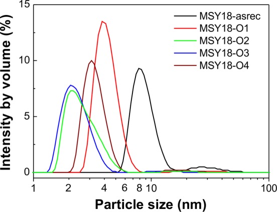
DLS distribution of MSY18 sample set taken as intensity by volume.
To roughly evaluate the yield of sub-5 nm NDs isolated by centrifugation from initial colloids, we used the procedure reported by Rehor and Cigler24 for MSY 25 powder. The MSY 25 powder has median size of 25 nm, which is close to the MSY 18 powder (median 18 nm) used in this work. The fraction of sub-5 nm HPHT nanodiamonds in the as-received MSY 25 powder was estimated to 33% (number-weighted distribution) from TEM image analysis; however, 33% of number-weighted distribution corresponds only to 0.4 wt %. We assumed similar distribution also in the MSY 18 powder. Because we used 20 mg of the MSY 18 powder for the preparation of the 1 mL colloids, 0.4 wt % from 20 mg corresponds to 80 μg, which was below detection limit of our laboratory scales. On the basis of the size distribution characteristics provided by Rehor and Cigler,24 we estimated the yield of sub-5 nm NDs to 5 μg of per 1 mg (i.e., 5 mg/g) of the initial powder after using the centrifugation step. Nevertheless, we obtained sufficient amount to be analyzed by XRD using MSY18-O3 dried colloidal solution. Comparison of (111) XRD peaks of DND and HPHT nanodiamonds (MSY18-O3) of similar size distribution is presented and discussed in Figure S1 in the Supporting Information. In brief, the peak of MSY18-O3 XRD peak matches that of monocrystalline diamond, while the DND-asrec XRD peak is asymmetric and shifted. In addition, the size obtained from XRD is underestimated for DNDs (3.2 nm) and overestimated for MSY nanodiamonds (7.2 nm).
To avoid the previously mentioned problems with XRD and DLS analysis, we performed AFM measurements that provide more accurate size values in both cases, including size distribution. Figure 2a shows the typical AFM image of the MSY18-O1 on Si substrate with the height distribution in the range of 0–10 nm. Figure 2b shows the processed AFM image after the particle size analysis procedure, which was used to obtain the accurate size distribution from the maximum particle height data. The size distribution statistics derived from the particle analysis is shown in Figure 2c,d as number versus particle size and as volume versus particle size, respectively. The same statistics of DND-asrec are shown for comparison. (For the AFM image, see Figure S2 in the Supporting Information.) The histograms show very similar size distribution of MSY18 and DND; that is, the number of sub-8 nm particles is dominant. Actually, from the number versus size histograms, it is obvious that the centrifugation keeps the mean MSY18 particle size around 3 ± 2 nm, which is even smaller than the DND size. Nevertheless, certain but not dominant fraction of larger (>8 nm) MSY18 NDs appears in volume versus size histograms due to their grinding origin. Despite a reported existence of single DNDs of up to 30 nm in size,35 we excluded larger particles (>8 nm) from the DND size distribution analysis because the typical size of DNDs is 5 ± 3 nm. It is clear that due to the grinding origin of MSY18 NDs the larger particles (>8 nm) cannot be ignored because they may still represent single particles. Nevertheless, their contribution to the volume distribution is not dominant for MSY18 samples, as shown in Figure 2d, which is in accordance with the DLS analysis. As a matter of course, it is not possible to securely distinguish between a single particle and agglomerate from the AFM data.
Figure 2.

AFM image (1 × 1 μm2, Z scale 15 nm) of MSY18-O1 on Si substrate after ultrasonic-assisted deposition from the colloidal solution (a). Corresponding AFM image of MSY18-O1 after the particle analysis procedure (b). Size distribution histograms by number (c) and by volume fraction (d) of the DND and MSY18 NDs as derived from the AFM particle analysis.
In Figure 3a the TGA curves of MSY18, and DND NDs (raw powders, no annealing/centrifugation) are shown. The TGA curves of both types of NDs can be divided to four temperature regions. In the first region “I” (25–150 °C), an initial decrease in weight due to desorption of adsorbed water is observed. This region is magnified in the inset of Figure 3a, showing ∼3 wt % of water in MSY18, and DND. In the second region “II” (150–300 °C), the weight of both the MSY18 and DND is more or less constant. In the third region “III”, an increase in the weight of DND is observed having a maximum around 450 °C. When the DND particles were annealed at 450 °C for 30 min prior to the TGA measurement, they become fully oxidized and did not exhibit any increase in this region any more (TGA curve not shown here). This indicates an oxidation of “light” C–H bonds31 to “heavier” C=O or C–O bonds. In contrast, the MSY18 seems to be already fully oxidized, as they do not exhibit any increase in their weight; that is, they do not contain any C–H bonds and gradually decrease their weight, which indicates nondiamond phase removal. In the fourth region (>500 °C) “IV”, a pronounced steep decrease in weight of both MSY18 and DND samples occurs due to etching of diamond via oxidation in air. The temperature where the oxidative etching of diamond phase starts can be roughly extracted from the TGA curves. These temperatures are 450 °C for MSY18 and 480 °C for the DND. The lower temperature found for MSY18 indicates the presence of very small particles (sub-5 nm) that etch away faster than the larger particles due to their high surface-to-volume ratio. Also, various surface or lattice defects induced by grinding process may lower the oxidation temperature. DNDs exhibit a steeper decay of weight than MSY18-asrec due to their narrower size distribution, and their decomposition is finished at 780 °C. In contrast, the decomposition of the MSY18 is not finished until 800 °C due to broader size distribution.
Figure 3.
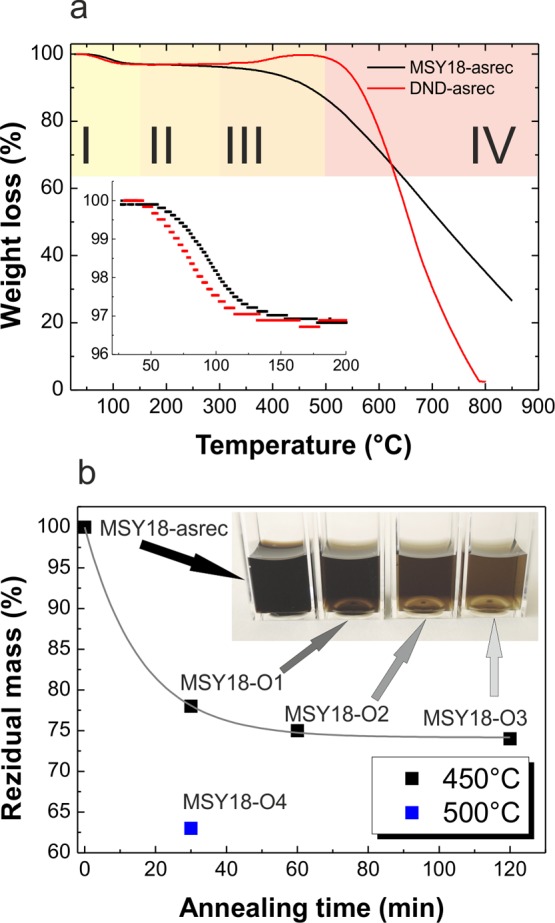
TGA curves of MSY18-asrec and DND-asrec with four temperature regions indicated. The inset shows the initial weight loss due to water evaporation. (a). Weight loss versus annealing time curve at 450 °C (MSY18-O1-3, black squares) and at 500 °C, 30 min (MSY18-O4, blue square) shown with corresponding colloidal solutions (b).
Figure 3b shows an exponential decay of the MSY18 mass with time during annealing at 450 °C. It is obvious that after 120 min of annealing at 450 °C the mass decay almost stops at ∼75% of the initial weight. The temperature of 450 °C was chosen in consensus with the TGA curve because above this temperature the weight loss accelerates, which points out the direct oxidative etching of diamond phase. Indeed, it is shown that the weight decreases to 63% after annealing at 500 °C for only 30 min (MSY18-O4).
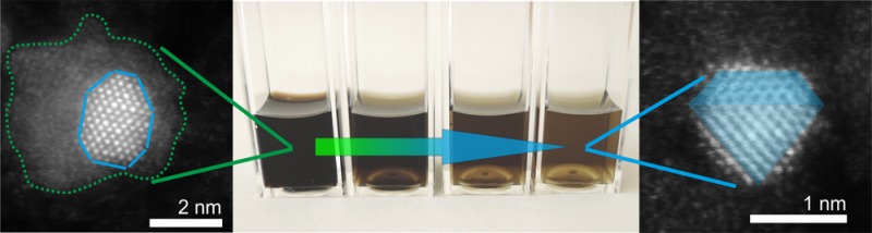
Representative STEM image of a nonannealed MSY18-asrec sub-10 nm NDs is shown in Figure 4a,b. Besides the ∼2 nm crystalline diamond core, an irregular amorphous shell around the NDs is visible (Figure 4a,b). Figure 4a can be identified as the diamond particle projected along the (110) direction, where the [111] and [002]-type reflections (2.06 and 1.78 Å spacing, respectively) are visible and apparent in the Fourier transform. Figure 4b is identified as a projection along (001), where the 1.78 Å spacing of the [002] type reflections is the largest visible periodicity. Interestingly, the amorphous shell around this ND seems to be reduced from the top and flattened more on the sides of this particular particle. Because the ND is deposited on the well-conductive monatomic layer of graphene, the low-density material charged with electron beam might be attracted to the graphene substrate during electron scanning. On the contrary, the particle in Figure 4b seems to be surrounded with the amorphous layer also from the top side. It is indicated from a slightly disturbed atomic order in the direct image (Figure 4b) as well as from the blurred FFT pattern shown in the inset. Figure 4c,d shows a representative sub-1.5 nm NDs with no apparent amorphous shell as a result of air annealing. They can again be identified as diamond particles projected along (110), although a small mistilt appears to be present in Figure 4c. Figure 4d, in particular, shows one of the smallest ND identified having size of 1.1 nm. The diamond character of these NDs is confirmed by the FFT patterns shown in insets, which show clear symmetry corresponding to different orientations of the NDs and good agreement with the well-ordered crystal structure of diamond. Comparison of STEM images of representative detonation and HPHT nanodiamonds is provided in the Figure S3 in Supporting Information.
Figure 4.
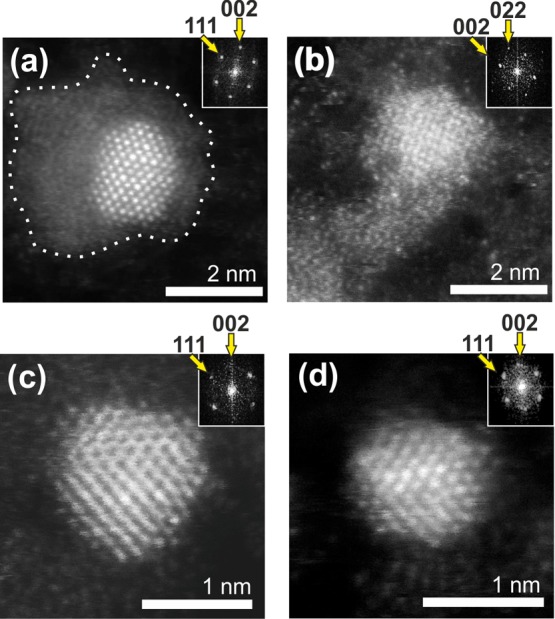
STEM images and related FFT data (insets) of representative MSY18 NDs. MSY18-asrec ND showing a diamond core surrounded by an amorphous nondiamond carbon shell (a,b). Ultrasmall, sub-1.5 nm MSY18-O3 NDs after efficient removal of the nondiamond carbon shell by air-annealing (c,d).
Surface chemical composition and sp2/sp3 carbon content of the MSY18 NDs were analyzed by XPS. Figure 5 shows the deconvoluted C 1s XPS spectra of the original MSY18 as-received NDs prior to the centrifugation, MSY18-asrec, and MSY18-O1. The spectra of the C 1s peak were deconvoluted into four peaks: C-sp2 (284.2 eV),33 C-sp3 (285.3 eV),34,36 C–O (286.6 eV), and C=O (287.6 eV).37 The deviation of binding energies in the deconvolutions was in the range of ±0.2 eV.
Figure 5.
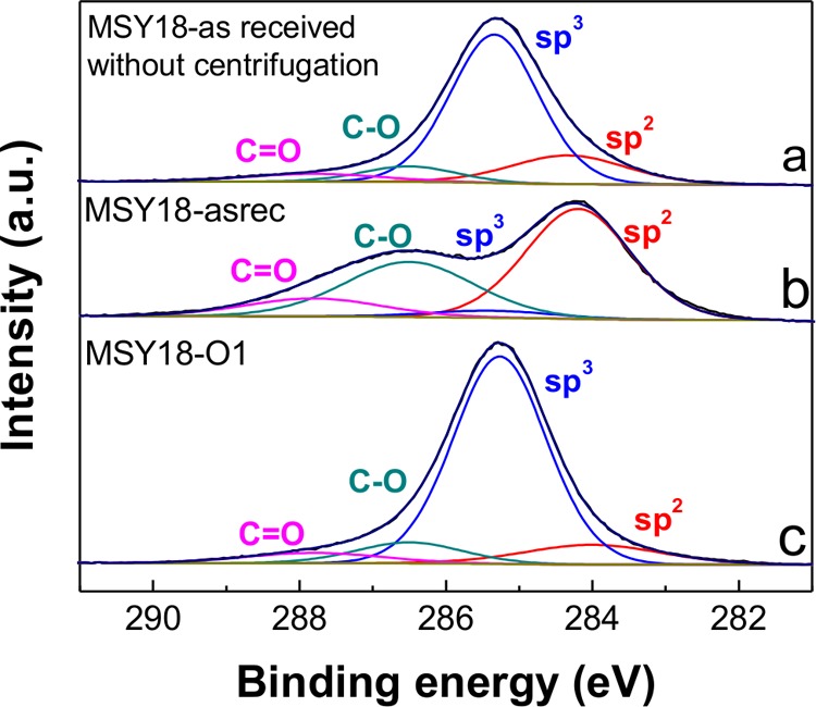
Deconvoluted C 1s spectra of MSY18 as-received powder prior to centrifugation (a), centrifuged MSY18-asrec (b), and annealed (30 min) and centrifuged MSY18-O1 (c).
The concentration of particular elements and chemical bonds as determined by XPS is summarized in Table 1. The main identified elements were oxygen and carbon. Traces of other elements were not detected except for a trace amount of nitrogen (<1%), which was not included in the compositional calculation. The signal from Si substrate was screened by a thick enough ND layer.
Table 1. Elemental Composition and Concentration of the Chemical Bonds (Carbon Hybridization and Oxygen Bonding) of MSY18 NDs as Derived from the XPS Analysis.
| sample name | O (%) | C (%) | sp2 (%) | sp3 (%) | C–O (%) | C=O (%) |
|---|---|---|---|---|---|---|
| MSY18-asrec, prior to centrifugation | 13 | 87 | 17 | 69 | 8 | 6 |
| MSY18-asrec | 12 | 88 | 52 | 4 | 33 | 11 |
| MSY18-O1 | 13 | 87 | 10 | 76 | 9 | 5 |
| MSY18-O2 | 15 | 85 | 9 | 74 | 10 | 7 |
| MSY18-O3 | 14 | 86 | 9 | 76 | 9 | 6 |
| MSY18-O4 | 16 | 84 | 9 | 74 | 8 | 9 |
The XPS data show a slight increase in the total oxygen content in the MSY18 NDs after the air annealing (Table 1). From the deconvoluted XPS spectra of the carbon C 1s peak (Figure 5), it is obvious that the initial MSY18 as-received NDs already contain considerable amount of nondiamond sp2 phase (17%). As soon as the MSY18 as-received sample is analyzed after centrifugation (MSY18-asrec), the sp2 content further increases to 52%, while the sp3 content decreases to only 4%. This indicates very low concentration of real NDs in the MSY18-asrec sample, which is instead composed of sp2 carbon nanoparticles or NDs heavily covered by sp2 carbon. (See Figure 4a.) These as-received particles (sub-10 nm according to AFM) are nevertheless well-oxidized, as suggested by totally 44% of C–O bonds detected by XPS. It is expected that the oxygen-containing surface functional groups are located on the surface of these carbon nanoparticles and its high concentration is a sign of the high surface-to-volume ratio of the sub-10 nm fraction. In accordance with the mass analysis, the sp2 content is greatly reduced already after 30 min annealing at 450 °C. Longer annealing time does not lead to further significant decrease in the sp2 content according to the XPS data.
The evolution of the surface chemistry as a function of air-annealing was also corroborated by the FTIR spectroscopy (Figure S4). As-received HPHT NDs contain epoxy and carboxylic acid groups that are the most probably a result of a treatment in strong acids at elevated temperatures during the fabrication process. The air-annealing leads to carboxylation and hydroxylation of the diamond core as well as to further formation of anhydrides and lactones, while the initially sp2-bonded epoxy and carboxylic acid groups are removed together with the amorphous graphitic shell. See the Supporting Information for more details.
The photoluminescence spectra of the studied samples are shown in Figure 6. The PL spectra are composed of two broad peaks centered at around 430 and 520 nm, respectively. The intensity ratio depends on the sample treatment (time and temperature of annealing). The PL spectrum of the MSY18-asrec sample is dominated by the second component at 520 nm, and the 430 nm component manifests itself only as a high-energy shoulder. Because the MSY18-asrec NDs are annealed at 450 °C, the overall PL intensity decreases and the PL spectrum changes. The initially dominant peak at 520 nm decreases with annealing time, while the peak at 430 nm starts to dominate the spectra of MSY18-O3 and MSY18-O4 samples. Because diamond has an energy band gap of 5.5 eV, that is, there is no band gap excitation at 355 nm, it is realistic to attribute these phenomena to modifications of functional groups on nanodiamonds. It is worth mentioning that C=O and OH functional groups alone in organic solvents such as alcohol and acetic acid do not give out light. Nevertheless, bound to the nanodiamonds backbone, the formation of some special conformations can be facilitated by the combination of hydroxyl groups and carbonyl groups in the vicinity of the edge of carbon nanomaterials.38 The time-resolved spectra of MSY18-asrec (Figure 6b) and MSY18-O4 (Figure 6c) show a different kinetics of both the 520 and 430 nm photoluminescence peaks. While the 520 nm peak has a slower decay (tens of nanoseconds) the peak at 430 nm exhibits an order of magnitude shorter (nanoseconds) decay time. This measurement indicates that the origin of the two PL peaks is different.
Figure 6.
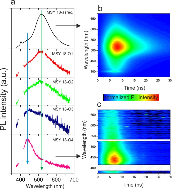
Photoluminescence spectra of MSY18-asrec (black), MSY18-O1 (red), MSY18-O2 (green), MSY18-O3 (dark blue), and MSY18-O4 (magenta) (a). PL kinetics of the MSY18-asrec (b) and MSY18-O4 (c). Blue vertical line is depicted at the spectral position of the PL peak attributed to surface functional groups present on purified NDs, whereas the green vertical line is plotted at the position of the PL related to functional groups bonded to sp2 carbon. In the case of MSY18-O1-4, spectral regions at around 400 and 520 nm were strongly contaminated by the Raman peak of the water and by the second harmonic of the excitation laser, respectively, and thus they were omitted from the plot.
The UV-Raman spectra of the MSY18 as well as DNDs are shown in Figure 7. Two main features dominate the Raman spectra of both kinds of NDs—the diamond peak at 1330 cm–1 for MSY18 and 1323 cm–1 for DND corresponding to the first-order excitation of the triply degenerate (F2g) optical phonon at the Brillouin-zone center39 and a broad band feature (1500–1800 cm–1) commonly ascribed to the presence of a graphitic carbon.40,41 Let us focus on the diamond peak first. Besides the large shift of diamond peak of DND samples (−10 cm–1 vs monocrystalline diamond standard), it also shows significant asymmetric broadening to lower wavenumbers (fwhm = 40 cm–1) with a sideband at ∼1250 cm–1. These spectral features are characteristic for UV Raman spectra of NDs of detonation origin.26,42 On the contrary the diamond peak of MSY18 NDs exhibits only a minor shift (−3 cm–1) and broadening (fwhm = 15 cm–1) in comparison with the monocrystalline diamond standard. It is important to emphasize here that because we measured spectra of MSY18 samples after centrifugation, we deal with a very similar size distribution of the MSY18 and DNDs. (See the DLS and AFM data.)
Figure 7.
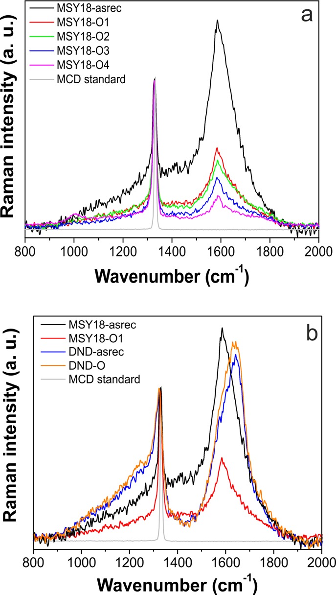
(a) UV Raman spectra of the MSY18 NDs (after centrifugation) showing considerable increase in the diamond peak intensity over the broad sp2-related band 1500–1800 cm–1 of the annealed samples. (b) Raman spectra of centrifuged MSY18 and DNDs before (MSY18-asrec, DND-asrec) and after the same annealing treatment (MSY18-O1, DND-O; 450 °C, 30 min). Reference spectrum of monocrystalline diamond (MCD, 1332.8 cm–1, fwhm = 8.9 cm–1) is shown for comparison.
The second dominant feature in the Raman spectra is a broad band rising between 1500 and 1800 cm–1. It has been shown that it might be composed of at least three overlapping peaks: G-band at 1590 cm–1 from in plane vibrations of graphitic carbon, a peak centered around 1640 cm–1 that has been ascribed either to O–H bending vibrations from the adsorbed water43 or to small sp2 fragments,40,42 and a shoulder at 1760 cm–1 related to stretching the surface C=O functional groups.43 The Raman spectra unambiguously confirm that the MSY18-asrec sample contains a high amount of nondiamond carbon sp2 phase as the broad band with maximum at 1590 cm–1 has higher intensity than the diamond peak at 1330 cm–1. Figure 7a, at the same time, perfectly demonstrates that already after 30 min annealing at 450 °C the diamond peak becomes dominant. The longer annealing times lead to further decrease in 1500–1800 cm–1 band intensity. Moreover as soon as the temperature of the annealing is raised to 500 °C (MSY18-O4), the 1500–1800 cm–1 band is further suppressed.
In the case of DNDs, the band at 1500–1800 cm–1 has a maximum at 1640 cm–1 (O–H or sp2) with the G-band (1590 cm–1) and C=O (1760 cm–1) related peaks as shoulders. Raman spectra clearly confirm different inner or surface structure of the MSY18 and DNDs of similar size. It is evident that while the air annealing of MSY18 at 450 °C for 30 min already reduces the graphitic content considerably, the same treatment does not lead to any significant change of DNDs.
Discussion
1. Size Control
Centrifugation has already been used before for fractionation of NDs.16,18,25 In the case of DND, nearly monodispersed distribution of single particles is possible to achieve44 because the size distribution of DND is already narrow. Another study showed that centrifuge acceleration to 8.65 × 10⁴g for 40 min can provide NDs with median size of 4 nm starting from a HPHT material with median size of 30 nm.25 Our results show that the HPHT material of 18 nm median size is more advantageous due to the possibility of using a common table-top centrifuge to separate the sub-10 nm ND fraction. The AFM particle analysis of all centrifuged MSY18 samples (Figure 2c) showed that their size distribution is very similar to the size distribution of DNDs.
Nevertheless, we noticed a certain discrepancy between the DLS and AFM data. In particular for the MSY18-asrec sample the DLS shows larger sizes than detected by AFM. This may be caused by the fact that DLS technique measures the value of hydrodynamic diameter, i.e., also a hydration shell contributes to the measured diameter value. Purification treatment of the MSY18 powder involves oxidation treatment in aqua regia (HNO3/HCl, private correspondence with O. Kaderli from Microdiamant AG), which results in the removal of the metallic impurities after the grinding process and oxidation of the sp2 carbon phase (not to its removal), as evidenced by the detection of C–OH, C=O, and C–O–C bonds in the MSY18-asrec powder. (See XPS and FTIR data.) Thanks to these chemical bonds a water adsorption or intercalation may occur in the oxidized sp2 phase when stored under ambient conditions (3 wt % indicated by the TGA). The dispersion of such particles in water then may lead to a certain swelling of the disordered graphitic material or to the formation of a relatively thick hydration shell around the MSY18-asrec NDs. That is why we employed two independent techniques such as DLS and AFM to carefully evaluate the particle size distribution.
The particle size was further influenced by annealing treatment. Note that centrifugation is performed after the annealing. Thus, the histograms contain about the same size of NDs as determined by their weight, centrifugation speed, and duration; however, their material composition is different, as clearly shown by Raman, FTIR, PL, and STEM.
There is also a slight but noticeable shift of number versus size histogram to the larger sizes with the annealing. This indicates that smaller NDs (∼3 nm) are etched (i.e., cleaned and/or reduced in size) more efficiently than larger particles. Indeed, this is confirmed by emergence of a double peak in MSY-O4 histogram, which shows two dominant sizes: 5 and 1.5 nm. The sub-2 nm fraction must arise from a size reduction of larger NDs, as such small diamond particles are not initially detected. The annealing at 500 °C thus most likely leads not only to graphitic phase removal but also to considerable etching of diamond phase. Such an effect was indeed detected by TGA and mass analysis. (See Figure 3.) The different etching efficiency as the function of particle size can be explained by the nonlinear dependence of surface-to-volume (S/V) ratio toward smaller particle sizes. Specifically, the S/V ratio can be estimated to 1.2 for 5 nm, 2 for 3 nm, and 4 for 1.5 nm particles.
True diamond character of the sub-2 nm particles is not directly obvious, though. Nondiamond particles would not withstand the etching process, yet they could newly arise due to instability of diamond particles < ∼2 nm, which is presumed during the detonation or plasma CVD process for diamond growth. More specifically, theoretical calculations predict a transformation of a ND into a bucky diamond (nanoparticle with a diamond core surrounded by fullerene shells) as its size decreases below 2.2 nm,45 and determine a window of stability for ND to be in the range of approximately 1.9–5.2 nm.46 More recent theoretical results show a strong dependence of the fraction of sp3, sp2+x, and sp2-bonded carbon atoms on ND shape (octahedral, truncated octahedral, cuboctahedral and cuboid shapes) in the 1–3.3 nm range;47 however, in the mentioned calculations, no air-annealing was involved. It was theoretically shown that the primary role of oxygen is the saturation of surface carbon atoms and the etching of the graphitic part, that is, to increase the sp3 ratio. It was suggested that if [200]-faceted NDs as small as 1 nm in diameter are formed during synthesis, they will be kinetically stable up to 1500 K.48 Such theoretical predictions are in good agreement with our experimental observations. For instance, the STEM images (Figure 4c,d) clearly show stable HPHT NDs as small as 1.1 nm with [111] facets and no apparent nondiamond shell. More details of the ND material quality and surface chemistry are discussed in the following section.
2. Purity Control
Achieving the small size of NDs is only the first step, though. Wherever well-defined NDs are needed, the considerable sp2 nondiamond phase (∼25 wt %) found in MSY18 as-received NDs (Figure 3b) might represent a severe obstacle. The centrifugation alone led only to further accumulation of the nondiamond carbon, as directly identified by XPS (Figure 5) and Raman spectroscopy (data not shown). The nondiamond carbon obviously comes from the grinding process. The high-energy impact of the grinding beads leads to cleavage of the diamond micro/nanocrystals and to the generation of dangling bonds at the new surface. This promotes the reconstruction of the particle surface to sp2 disordered carbon. The resulting sp2 carbon nuclei lead to the subsequent formation of more extended areas of graphitic material on the particle surfaces due to local heating in the milling mixture.49,50 Pressure-induced graphitization (pressure exceeding 900 GPa)51,52 of the smallest, originally diamond particles certainly contributes to the disordered graphitic material formation as well.
To purify the NDs, we can use a simple approach based on the annealing in the ambient air. The air-annealing of the DNDs is already a well-established technique not only for removing the nondiamond graphitic content but also for terminating their surface with oxygen-containing groups at the same time.28,31 The most suitable temperature–time range reported is 400–430 °C applied for 5 h, resulting in the oxidation of sp2-bonded carbon with no or minimal loss of diamond.26 On the basis of the TGA experiments, we chose the temperature of 450 °C, which enables us to use a shorter time for the sp2 phase removal. Indeed, efficient purification of the MSY18 NDs is evidenced by the XPS, STEM, PL, and Raman spectroscopy, which all show a substantial decrease in the sp2 phase content already after 30 min of the annealing treatment at 450 °C. The purification progress is visualized by STEM. STEM showed the core–shell structure of a ND prior to the annealing (Figure 4a) as well as well-defined clean NDs without any apparent disordered sp2 carbon shell after the annealing (Figure 4b–d). The core–shell structure of the untreated MSY18-asrec NDs is obviously responsible for the differences in XPS and Raman analysis. XPS is a very surface-sensitive technique, which in the case of centrifuged MSY18-asrec predominantly detects the surface sp2 carbon from the outer shells because the attenuation length of X-rays of used energy (1486.6 eV) is ∼3.5 nm for carbon.53 On the contrary, Raman spectroscopy also probes the volume of a sample, and thus both sp2 and sp3 carbons were detected in the MSY18-asrec sample.
The results of the PL experiments (Figure 6) correlate very well with the interpretation of structural and surface chemistry changes as a function of the annealing process. The PL component at 520 nm can be obviously assigned to the nondiamond phase with specific surface functional groups such as epoxy/carboxylic groups, the content of which is strongly reduced when the MSY18 NDs are annealed at 450 and 500 °C. On the contrary, the blue PL peak at 430 nm being originally a mere shoulder in the MSY18-asrec spectrum became dominant in the MSY18-O4 (500 °C, 30 min) spectrum. A similar blue-green PL (UV excitation) has been observed in graphene nanodots prepared in different oxidation states. While fully oxidized graphene nanodots with −COOH and C–O–C groups exhibited a green PL, the reduced graphene nanodots with −OH groups exhibited a blue PL.54 The most recent study of surface chemistry-dependent PL study on nanodiamonds also assigned a blue PL component to the −OH bond bound to nanodiamonds.55 Thus, the 520 nm green peak originates from the −COOH and C–O–C groups mainly bonded to sp2 amorphous shell, while the blue PL peak at 430 nm most probably originates from −OH moieties bonded to exposed diamond core. This assignment is in good agreement with evolution of surface-functional groups as a function of the annealing time and temperature, as evidenced by FTIR. (See Figure S4.)
Alternatively, the origin of the blue PL peak at 430 nm could be ascribed to the A band, which is one of the most characteristic luminescence features of diamond. Its decay time is typically below 10 ns,56 which is in a good agreement with our data in Figure 6c. While diamond itself should have no visible PL due to its wide band gap, this dislocation-related PL feature having a maximum at ∼430 nm is readily observed in natural diamonds, CVD diamond films, and HPHT synthetic diamonds.57 The presence of dislocations in the NDs may be indicated, for instance, by the broadening of diamond Raman peak compared with the monocrystalline sample. (See Figure 7.) Because the HPHT NDs are made by grinding process of HPHT microcrystals, it is likely that in addition to the already present dislocations in the original microcrystals, new ones can also be formed during the grinding process; however, if the blue PL peak at 430 nm arises from the A band it should emerge immediately after the first 30 min of annealing, as most of the nondiamond phase is removed. This is not observed, and rather a step-like increase is observed in the MSY18-O4 sample. Thus, it is most probably connected to the –OH bonds formation, as evidenced by FTIR.
UV-Raman spectroscopy (Figure 7) confirms graphitic carbon (G-band, 1590 cm–1) as the main component in the MSY18-asrec sample in accordance with the XPS analysis. The efficient removal of the graphitic carbon and thus purification of NDs by means of air annealing is evidenced by the decreasing the G–band (1590 cm–1) intensity, although the G-band signal does not fully disappear even after annealing at 500 °C for 30 min (MSY18-O4), again in accordance with the XPS analysis. At this temperature, an oxidation of the sp3 diamond phase already occurs (see TGA data), and thus it cannot be the original nondiamond shell. This leads us to the conclusion that the residual signal from the graphitic phase in Raman as well as XPS spectra comes from sp2 surface carbon atoms, which may be present especially on [111] planes of NDs. Indeed, STEM FFT patterns indicated [111] orientation of our HPHT NDs.
In contrast with HPHT NDs, Raman spectra of DND exhibit the broad band between 1500 and 1800 cm–1 with a maximum at 1640 cm–1, while the G band is present only as a shoulder. Moreover, the air annealing at 450 °C, 30 min of DND does not lead to any reduction of this band intensity or a change of its shape. It means that the shell of DND-asrec NDs has different and more complex structure than that of MSY18 NDs.
It was repeatedly reported that the diamond core of DNDs is covered by a surface shell that is formed during the explosion. The 1640 cm–1 Raman peak was ascribed to a mixed sp2/sp3 carbon structure,58 or it was referred to as a peak of “sp2 carbon”59 or “sp2 clusters”40 without any explanation regarding the structure. D′ peak (1620 cm–1) as it appears in nanocrystalline graphene60 may also contribute to this band. Pichot et al.27 performed a comprehensive study of air-annealing purification of DNDs, and despite very clean final DND product, the thickness of the nondiamond carbon shell, which still covered the ND surface, was estimated to be 0.345 nm. Pawlak et al.61 showed by means of scanning tunneling microscopy the presence of both ordered relaxed surfaces attributed to C[111] or graphene and disordered chain-like graphitic structure present on DNDs surface. Because of rapidly changing nonequilibrium conditions during the detonation process, also a transient sp3/sp2 layer between the diamond core and graphitic shell was suggested for the DNDs.17 While the utmost graphitic layer is accessible for the removal via air oxidation, the transient sp3/sp2 layer probably persists on the diamond core after the air oxidation. Obviously, the MSY18 NDs do not contain such transient sp3/sp2 layer, and the graphitic shell can be efficiently removed by the air annealing.
The 1640 cm–1 Raman peak was also suggested to originate from bending O–H vibration coming from adsorbed water based on Raman and FTIR experiments on DNDs despite a very weak Raman cross section of water.43 Mermoux et al.42 recently performed a multiwavelength Raman spectroscopy study and showed that Raman spectroscopy is actually rather insensitive to the surface chemistry of DNDs and concluded that the whole 1500–1800 cm–1 region in Raman spectrum indeed comes from a nondiamond carbon. We believe that our results support those of Mermoux et al.,42 as Figure S4 (see Supporting Information) shows that the FTIR spectra of both MSY18-O1 and DND-O NDs after the same annealing treatment exhibit the presence of O–H bending vibrations (1625 cm–1). Its intensity seems to be even higher in the MSY18-O1 spectrum. Thus, the obvious difference in the 1500–1800 cm–1 region of the MSY18-O1 and DND-O Raman spectra cannot be satisfactorily explained by adsorbed water because both MSY18-O1 and DND-O NDs have similar sizes (unless there is a significantly different water adsorption between DNDs62 and HPHT-NDs).
3. Phonon Confinement
Another striking difference between the Raman spectra of MSY18 and DNDs is the different shape of the diamond peak. While the diamond peak of the annealed MSY18 NDs resembles that of monocrystalline diamond, a strong shift toward the excitation-laser line, asymmetric broadening, and a low-frequency shoulder of diamond peak are typical features observed in Raman spectra of the DNDs. Depending on the peak shift and broadening, the Raman spectroscopy has often been used even as a tool for size determination of, for example, Si,63,64 TiO2,65 and ZnO66 nanocrystals using the phonon confinement model.67,68
Also, for DNDs, the shift and asymmetric broadening are regularly explained by phonon confinement effect due to the small size of the DNDs (∼5 nm); however, the origin of the shoulder at 1250 cm–1 remains speculative. On the basis of the Raman investigation of diamond-like carbon films, Merkulov et al.69 and Prawer et al.70 assigned this shoulder to amorphous diamond, that is, to a disordered structure of sp3-hybridized units. On the contrary, Mykhaylyk et al.58 and Osswald et al.71 suggested that not only the shift and asymmetric broadening of the diamond peak but also its low-frequency shoulder originate from the phonon confinement effect in smaller coherent scattering domains separated by defects in DNDs. In brief, the phonon-confinement model (PCM) took into account contributions from phonons away from the center of the Brillouin zone, which may start to contribute to Raman spectrum if a scattering domain (nanoparticle) is sufficiently small; however, this explanation is problematic due to following reason: Most often the 2D defects present in the DNDs are the twin boundaries, leading up to even 5-fold twin structure, as identified by HRTEM.71,72 Then, each grain can be considered as an independent domain and may contribute to the phonon confinement effect, that is to a broadening and blue shift of the diamond line, but because the DNDs are not strictly monodisperse, a smooth broadening of the diamond peak to lower wave numbers is reasonable to expect. (Particles of different sizes have scattering domains of different sizes, and an overlap has to occur.) This is in disagreement with the real Raman spectra of DNDs, in which the 1260 cm–1 band is typically detected as a sideband.
The Raman diamond peak blue shift down to 1323 cm–1 and broadening to 32 cm–1 as predicted by the PCM41 roughly correlates with values extracted from our DND Raman spectra as well as with the results reported by other groups.41,42,71 On the contrary, the fitting of diamond peak of HPHT NDs (MSY18-O1) according to frequently used PCM modification of Yoshikawa41 (see the blue curve in Figure 8) resulted in the size of scattering domain of 10.8 nm, while the volumetric mean size evaluated from AFM is 6.3 nm. Thus, the use of the simple approach of Yoshikawa41 leads to inaccurate values of the mean ND size estimation. In general, sufficiently accurate estimation of mean particle size from single spectral measurement can be done only for ideal size distributions such as normal or log-normal.
Figure 8.
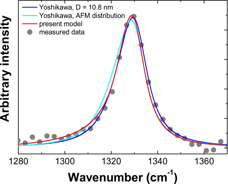
Diamond peak line shape of MSY18-O1 NDs fitted by the approach of Yoshikawa, equations S2 and S4 in the Supporting Information (blue curve). The fitted parameters of the red curve are fwhm = 12 cm–1, D = 10.8 nm. The approach of Yoshikawa involving the AFM distribution and fwhm =8.9 + 6.88/D (cyan curve). Simulated diamond peak line shape of MSY18-O1 NDs by the modified PCM model using the measured AFM size distribution (red curve, equations S6 and S7 in the Supporting Information).
It may be objected that the larger NDs may mask the phonon confinement effect in HPHT NDs as the Raman signal is directly proportional to the volume of particles; however, we have shown by the AFM particle size analysis that the main volume fraction is concentrated between 3 and 8 nm (∼70%) and the rest of the region 8–14 nm has somewhat flat volumetric distribution. Incorporating this measured size distribution into the Yoshikawa model gave an even worse fit of the measured diamond peak. (See the light blue curve in Figure 8.)
Osswald et al.71 modified the PCM by fitting the contributions of seven individual phonon modes to fit not only the diamond peak but also its low-frequency shoulder. With each phonon mode, independent particle (or domain) size was fitted; however, this approach led to the size between 1.8 and 3.9 nm for five phonon modes but to 11.3 and 17.4 nm for the other two phonon modes. In our opinion, the contribution of the larger domain size cannot be ignored in any phonon mode. Also, the weighting of particular phonon branches is not clear. Thus, although the approach of Osswald et al.71 leads to more accurate fits, it cannot be used to determine the mean particle size. For such a purpose, the model can be modified under the assumption that NDs do not contain coherent domains that are smaller than their size. (See the Supporting Information for more details.) Under this assumption, all phonon modes equally contribute to the Raman scattering because virtually no crystallographic direction is preferred in the ensemble of approximately spherical NDs. It can be seen in Figure 8 that the shape of the measured MSY-18-O1 diamond peak can now be reconstructed without any fitting, just using the measured volumetric particle size distribution (red curve). It means that the slightly asymmetric shape and minor blue shift of the peak could be indeed explained by real phonon confinement effect in the HPHT (MSY18) NDs.
Because the DNDs have very similar volumetric size distribution to the MSY-18 centrifuged particles, other effects must be considered to explain much larger blue-shift, asymmetric broadening, and distinct low-frequency shoulder of the DND diamond peak compared to HPHT NDs. For example, laser-induced heating was shown to influence the diamond peak maximum of HPHT NDs.73 However, for DNDs this effect was negligible. It has also been shown by experiments with diamond anvil that the Raman diamond peak broadens and shifts to higher energies by application of a compressive stress.74 The opposite shift observed here may indicate a tensile stress due to certain lattice distortion. Using XRD, Yurev et al.75 has shown that quality of DNDs may be assessed by measuring lattice distortion compared to natural diamonds. Indeed, various lattice distortions were frequently found in DNDs from various manufacturers. Thus, we assume that the anomalies in the Raman spectra of DNDs are most likely due to various defects (point defects, lattice defects, scattering domains) rather than to phonon confinement in perfect diamond nanocrystals.
4. Model of Size and Purity Control
We can summarize the above data and findings by assembling a schematic model of the size and purity control by air annealing of HPHT NDs. The model is shown in Figure 9. At first, there is a high concentration of graphitic carbon in the MSY18-asrec NDs. Larger particles have a core–shell structure with a diamond core surrounded by a graphitic layer, while the smallest MSY18-asrec nanoparticles dominantly consist of sp2 amorphous carbon. As we demonstrated for larger particles, the graphitic shell becomes greatly reduced by the air annealing at 450 °C without affecting the diamond core, yet note that the annealing obviously reduces the overall particle size and thus in the given size range more purified NDs are collected in the supernatant after centrifugation (as indicated by the tilted black arrows). Hence, with the help of centrifugation, sub-10 nm NDs (mean size ∼3 nm) of excellent purity and crystallinity may be obtained. As the temperature of the air-annealing is increased to 500 °C, the oxidative etching of diamond is initiated, and a certain loss of diamond content is additionally observed. At the same time this produces a considerable amount of 1 to 2 nm NDs due to the size reduction of originally larger NDs (as indicated by the tilted red arrows).
Figure 9.
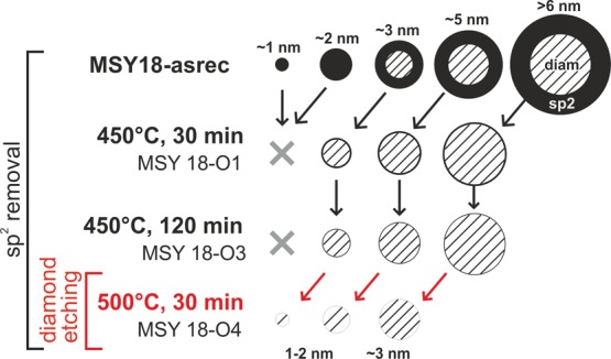
Schematic model of the sub-10 nm MSY18 NDs size distribution and composition before and after subsequent annealing at 450 °C. It shows gradual reduction of graphitic phase (black) content with annealing time, including removal of amorphous carbon dots. Size reduction of diamond core itself is also depicted for the annealing at 500 °C.
Conclusions
We presented a simple yet effective approach to control the size and purity of HPHT NDs below 10 nm by annealing in air and centrifugation. We showed that as-received NDs contain ∼25 wt % of nondiamond carbon in the form of stand-alone carbon dots and nanodiamonds thickly covered by amorphous sp2 carbon shell weakly bound to the diamond core. The amorphous sp2 carbon is efficiently removed by air annealing at 450 °C. This temperature was derived from the thermogravimetric analysis because it represents a boundary of the oxidative etching of diamond phase. After this purification treatment, dominant fractions of high-quality HPHT NDs as small as 3 ± 2 nm (i.e., at or even below DNDs typical size) were obtained by relatively short centrifugation treatment, as evidenced by AFM/DLS/STEM (size) and XPS/STEM/Raman spectroscopy (purity). Furthermore, we showed that this approach can provide a considerable amount of nanodiamonds as small as 1.1 nm, which are probably the smallest man-made nanodiamonds ever shown and characterized. This size already attacks a molecular level, yet it remains fully crystalline without any apparent nondiamond shell. These findings shift the stability region of the standalone nanodiamonds down to 1 nm. For instance, Vlasov et al. recently showed76 that NDs as small as 1.6 nm isolated from a meteorite are capable of housing stable photoluminescent silicon vacancy (SiV) color centers.77 In this context, our method offers a great advantage in employing easily available HPHT NDs for making high-quality molecular-sized luminescent NDs for numerous applications.
The direct comparison of the MSY18 and DNDs Raman spectra on similar particle size scale brought us a new insight into the phonon confinement in diamond. The slightly asymmetrically broadened diamond peak of the HPHT NDs was fully described by the phonon confinement model when the measured ND size distribution was taken into account. Contrary, the spectra of DNDs could not be fitted correctly by this model. The observed DND diamond peak anomalies (blue shift and broadening) are thus caused rather by scattering on small domains separated by defects or by other effects, including the lattice stress or material gradient (diamond core-sp3/sp2 transient layer). From this point of view, the Raman spectra of the annealed HPHT NDs can be considered as the direct evidence of their excellent diamond character down to 1 nm size, which may also enable further experimental studies of general quantum phenomena in diamond that was scarcely attempted so far due to lack of convenient material. Thus, they may represent a new quality standard among sub-10 nm NDs.
Acknowledgments
This research was financially supported by the project 15-01809S (GACR). We acknowledge Vitezslav Zima for thermogravimetric measurements, Karel Knizek for XRD measurements, and Ivan Pelant for fruitful discussions. J.C.M. acknowledges support from the European Research Council (ERC) Project No. 336453-PICOMAT. This work occurred in frame of the LNSM infrastructure.
Supporting Information Available
The Supporting Information is available free of charge on the ACS Publications website at DOI: 10.1021/acs.jpcc.5b05259.
Comparison of X-ray diffraction peak of (111) plane of MSY18-O3 and DND-asrec nanodiamonds, AFM topography image of DNDs on Si substrate, size distribution histogram derived from the AFM data showing mean particle size ∼4 nm, STEM images of single DND and HPHT nanodiamond particle, full range FTIR spectra and 1000–2000 cm–1 region of the MSY18 NDs before and after air-annealing, full range and 1000–2000 cm–1 region FTIR spectra of MSY18-O1 and UDD-O annealed under the same conditions, and modified phonon confinement model equations. (PDF)
The authors declare no competing financial interest.
Supplementary Material
References
- Shenderova O. A.; Zhirnov V. V.; Brenner D. W. Carbon Nanostructures. Crit. Rev. Solid State Mater. Sci. 2002, 27, 227–356 10.1080/10408430208500497. [DOI] [Google Scholar]
- Hui Y. Y.; Cheng C.-L.; Chang H.-C. Nanodiamonds for Optical Bioimaging. J. Phys. D: Appl. Phys. 2010, 43, 374021. 10.1088/0022-3727/43/37/374021. [DOI] [Google Scholar]
- Balasubramanian G.; Lazariev A.; Arumugam S. R.; Duan D. Nitrogen-Vacancy Color Center in Diamond - Emerging Nanoscale Applications in Bioimaging and Biosensing. Curr. Opin. Chem. Biol. 2014, 20, 69–77 10.1016/j.cbpa.2014.04.014. [DOI] [PubMed] [Google Scholar]
- Schrand A. M.; Hens S. A. C.; Shenderova O. A. Nanodiamond Particles: Properties and Perspectives for Bioapplications. Crit. Rev. Solid State Mater. Sci. 2009, 34, 18–74 10.1080/10408430902831987. [DOI] [Google Scholar]
- Tisler J.; Balasubramanian G.; Naydenov B.; Kolesov R.; Grotz B.; Reuter R.; Boudou J.; Curmi P. A.; Sennour M.; Thorel A.; et al. Fluorescence and Spin Properties of Defects in Single Digit Nanodiamonds. ACS Nano 2009, 3, 1959–1965 10.1021/nn9003617. [DOI] [PubMed] [Google Scholar]
- Mochalin V. N.; Shenderova O.; Ho D.; Gogotsi Y. The Properties and Applications of Nanodiamonds. Nat. Nanotechnol. 2012, 7, 11–23 10.1038/nnano.2011.209. [DOI] [PubMed] [Google Scholar]
- Stacey A.; Karle T. J.; McGuinness L. P.; Gibson B. C.; Ganesan K.; Tomljenovic-Hanic S.; Greentree A. D.; Hoffman A.; Beausoleil R. G.; Prawer S. Depletion of Nitrogen-vacancy Color Centers in Diamond via Hydrogen Passivation. Appl. Phys. Lett. 2012, 100, 071902. 10.1063/1.3684612. [DOI] [Google Scholar]
- Petráková V.; Taylor A.; Kratochvílová I.; Fendrych F.; Vacík J.; Kučka J.; Štursa J.; Cígler P.; Ledvina M.; Fišerová A.; et al. Luminescence of Nanodiamond Driven by Atomic Functionalization: Towards Novel Detection Principles. Adv. Funct. Mater. 2012, 22, 812–819 10.1002/adfm.201101936. [DOI] [Google Scholar]
- Fu K.-M. C.; Santori C.; Barclay P. E.; Beausoleil R. G. Conversion of Neutral Nitrogen-vacancy Centers to Negatively Charged Nitrogen-vacancy Centers Through Selective Oxidation. Appl. Phys. Lett. 2010, 96, 121907. 10.1063/1.3364135. [DOI] [Google Scholar]
- Smith B. R.; Gruber D.; Plakhotnik T. The Effects of Surface Oxidation on Luminescence of Nano Diamonds. Diamond Relat. Mater. 2010, 19, 314–318 10.1016/j.diamond.2009.12.009. [DOI] [Google Scholar]
- Cui S.; Hu E. L. Increased Negatively Charged Nitrogen-vacancy Centers in Fluorinated Diamond. Appl. Phys. Lett. 2013, 103, 051603. 10.1063/1.4817651. [DOI] [Google Scholar]
- Krueger A.; Lang D. Functionality is Key: Recent Progress in the Surface Modification of Nanodiamond. Adv. Funct. Mater. 2012, 22, 890–906 10.1002/adfm.201102670. [DOI] [Google Scholar]
- Dolmatov V. Yu. Detonation-synthesis Nanodiamonds: Synthesis, Structure, Properties and Applications. Russ. Chem. Rev. 2007, 76, 339–360 10.1070/RC2007v076n04ABEH003643. [DOI] [Google Scholar]
- Pichot V.; Comet M.; Risse B.; Spitzer D. Detonation of Nanosized Explosive: New Mechanistic Model for Nanodiamond Formation. Diamond Relat. Mater. 2015, 54, 59–63 10.1016/j.diamond.2014.09.013. [DOI] [Google Scholar]
- Pichot V.; Risse B.; Schnell F.; Mory J.; Spitzer D. Understanding Ultrafine Nanodiamond Formation Using Nanostructured Explosives. Sci. Rep. 2012, 3, 2159. 10.1038/srep02159. [DOI] [PMC free article] [PubMed] [Google Scholar]
- Ozawa M.; Inaguma M.; Takahashi M.; Kataoka F.; Krüger A.; Osawa E. Preparation and Behavior of Brownish, Clear Nanodiamond Colloids. Adv. Mater. 2007, 19, 1201–1206 10.1002/adma.200601452. [DOI] [Google Scholar]
- Baidakova M. V.Methods of Characterization and Models of Nanodiamond Particles. In Detonation Nanodiamonds: Science and Applications; Vul A., Shenderova O., Eds.; CRC Press: Boca Raton, FL, 2014. [Google Scholar]
- Boudou J.-P.; Tisler J.; Reuter R.; Thorel A.; Curmi P. A.; Jelezko F.; Wrachtrup J. Fluorescent Nanodiamonds Derived from HPHT with a Size of Less than 10 nm. Diamond Relat. Mater. 2013, 37, 80–86 10.1016/j.diamond.2013.05.006. [DOI] [Google Scholar]
- Schirhagl R.; Chang K.; Loretz M.; Degen Ch. L. Nitrogen-Vacancy Centersin Diamond: Nanoscale Sensors for Physics and Biology. Annu. Rev. Phys. Chem. 2014, 65, 83–105 10.1146/annurev-physchem-040513-103659. [DOI] [PubMed] [Google Scholar]
- Aharonovich I.; Castelletto S.; Simpson D. A.; Su C.-H.; Greentree A. D.; Prawer S. Diamond-based Single-photon Emitters. Rep. Prog. Phys. 2011, 74, 076501. 10.1088/0034-4885/74/7/076501. [DOI] [Google Scholar]
- Mohan N.; Tzeng Y.; Yang L.; Chen Y.; Hui Y. Y.; Fang C.; Chang H. Sub-20-nm Fluorescent Nanodiamonds as Photostable Biolabels and Fluorescence Resonance Energy Transfer Donors. Adv. Mater. 2010, 22, 843–847 10.1002/adma.200901596. [DOI] [PubMed] [Google Scholar]
- Beranova J.; Seydlova G.; Kozak H.; Benada O.; Fiser R.; Artemenko A.; Konopasek I.; Kromka A. Sensitivity of Bacteria to Diamond Nanoparticles of Various Size Differs in Gram-positive and Gram-negative Cells. FEMS Microbiol. Lett. 2014, 351, 179–186 10.1111/1574-6968.12373. [DOI] [PubMed] [Google Scholar]
- Chu Z.; Zhang S.; Zhang B.; Zhang Ch.; Fang; Ch-Y; Rehor I.; Cigler P.; Chang H-Ch.; Lin G.; Liu R.; Li Q.; et al. Unambiguous Observation of Shape Effects on Cellular Fate of Nanoparticles. Sci. Rep. 2014, 4, 4495. 10.1038/srep04495. [DOI] [PMC free article] [PubMed] [Google Scholar]
- Rehor I.; Cigler P. Precise Estimation of HPHT Nanodiamond Size Distribution Based on Transmission Electron Microscopy Image Analysis. Diamond Relat. Mater. 2014, 46, 21–24 10.1016/j.diamond.2014.04.002. [DOI] [Google Scholar]
- Morita Y.; Takimoto T.; Yamanaka H.; Kumekawa K.; Morino S.; Aonuma S.; Kimura T.; Komatsu N. A Facile and Scalable Process for Size- Controllable Separation of Nanodiamond Particles as Small as 4 nm. Small 2008, 4, 2154–2157 10.1002/smll.200800944. [DOI] [PubMed] [Google Scholar]
- Osswald S.; Yushin G.; Mochalin V.; Kucheyev S. O.; Gogotsi Y. Control of sp2/sp3 Carbon Ratio and Surface Chemistry of Nanodiamond Powders by Selective Oxidation in Air. J. Am. Chem. Soc. 2006, 128, 11635–11642 10.1021/ja063303n. [DOI] [PubMed] [Google Scholar]
- Pichot V.; Comet M.; Fousson E.; Baras C.; Senger A.; Le Normand F.; Spitzer D. An Efficient Purification Method for Detonation Nanodiamonds. Diamond Relat. Mater. 2008, 17, 13–22 10.1016/j.diamond.2007.09.011. [DOI] [Google Scholar]
- Shenderova O.; Petrov I.; Walsh J.; Grichko V.; Grishko V.; Tyler T.; Cunningham G. Modification of Detonation Nanodiamonds By heat Treatment in Air. Diamond Relat. Mater. 2006, 15, 1799–1803 10.1016/j.diamond.2006.08.032. [DOI] [Google Scholar]
- Cunningham G.; Panich A. M.; Shames A. I.; Petrov I.; Shenderova O. Ozone-modified Detonation Nanodiamonds. Diamond Relat. Mater. 2008, 17, 650–654 10.1016/j.diamond.2007.10.036. [DOI] [Google Scholar]
- Shenderova O.; Koscheev A.; Zaripov N.; Petrov I.; Skryabin Y.; Detkov P.; Turner S.; Van Tendeloo G. Surface Chemistry and Properties of Ozone-Purified Detonation Nanodiamonds. J. Phys. Chem. C 2011, 115, 9827–9837 10.1021/jp1102466. [DOI] [Google Scholar]
- Kozak H.; Remes Z.; Houdkova J.; Stehlik S.; Kromka A.; Rezek B. Chemical Modifications and Stability of Diamond Nanoparticles Resolved by Infrared Spectroscopy and Kelvin Force Microscopy. J. Nanopart. Res. 2013, 15, 1568. 10.1007/s11051-013-1568-7. [DOI] [Google Scholar]
- Ondič L.; Dohnalová K.; Pelant I.; Žídek K.; De Boer W. D. A. M. Data Processing Correction of the Irising Effect of a Fast-gating Intensified Charge-coupled Device on Laser-pulse-excited Luminescence Spectra. Rev. Sci. Instrum. 2010, 81, 063104. 10.1063/1.3431536. [DOI] [PubMed] [Google Scholar]
- Lesiak B.; Zemek J.; Jiricek P.; Stobinski L. Temperature Modification of Oxidized Multiwall Carbon Nanotubes Studied by Electron Spectroscopy Methods. Phys. Status Solidi B 2009, 246, 2645–2649 10.1002/pssb.200982268. [DOI] [Google Scholar]
- Haerle R.; Riedo E.; Pasquarello A.; Baldereschi A. sp(2)/sp(3) Hybridization Ratio in Amorphous Carbon from C 1s Core-level Shifts: X-ray Photoelectron Spectroscopy and First-principles Calculation. Phys. Rev. B: Condens. Matter Mater. Phys. 2001, 65, 045101–045109 10.1103/PhysRevB.65.045101. [DOI] [Google Scholar]
- Osswald S.; Havel M.; Mochalin V.; Yushin G.; Gogotsi Y. Increase of Nanodiamond Crystal Size by Selective Oxidation. Diamond Relat. Mater. 2008, 17, 1122–1126 10.1016/j.diamond.2008.01.102. [DOI] [Google Scholar]
- Popov C.; Kulisch W.; Bliznakov S.; Mednikarov B.; Spasov G.; Pirov J.; Jelinek M.; Kocourek T.; Zemek J. Characterization of the Bonding Structure of Nanocrystalline Diamond and Amorphous Carbon Films Prepared by Plasma Assisted Techniques. Appl. Phys. A: Mater. Sci. Process. 2007, 89, 209–212 10.1007/s00339-007-4092-8. [DOI] [Google Scholar]
- Beamson G.; Briggs D.. High Energy XPS of Organic Polymers: The Scienta ESCA 300 Database; Wiley: Chichester, U.K., 1992. [Google Scholar]
- Xiao J.; Liu P.; Li L.; Yang G. Fluorescence Origin of Nanodiamonds. J. Phys. Chem. C 2015, 119, 2239–2248 10.1021/jp512188x. [DOI] [Google Scholar]
- Solin A. S.; Ramdas A. K. Raman Spectrum of Diamond. Phys. Rev. B 1970, 1, 1687. 10.1103/PhysRevB.1.1687. [DOI] [Google Scholar]
- Chen P.; Huang F.; Yun S. Structural Analysis of Dynamically Synthesized Diamonds. Mater. Res. Bull. 2004, 39, 1589–1597 10.1016/j.materresbull.2004.05.009. [DOI] [Google Scholar]
- Yoshikawa M.; Mori Y.; Obata H.; Maegawa M.; Katagiri G.; Ishida H.; Ishitani A. Raman Scattering from Nanometersized Diamond. Appl. Phys. Lett. 1995, 67, 694. 10.1063/1.115206. [DOI] [Google Scholar]
- Mermoux M.; Crisci A.; Petit T.; Girard H. A.; Arnault J-Ch. Surface Modifications of Detonation Nanodiamonds Probed by Multi-Wavelength Raman Spectroscopy. J. Phys. Chem. C 2014, 118, 23415–23425 10.1021/jp507377z. [DOI] [Google Scholar]
- Mochalin V.; Osswald S.; Gogotsi Y. Contribution of Functional Groups to the Raman Spectrum of Nanodiamond Powders. Chem. Mater. 2009, 21, 273–279 10.1021/cm802057q. [DOI] [Google Scholar]
- Williams O. A.; Hees J.; Dieker Ch.; Jäger W.; Kirste L.; Nebel Ch. E. Size-Dependent Reactivity of Diamond Nanoparticles. ACS Nano 2010, 4, 4824–4830 10.1021/nn100748k. [DOI] [PubMed] [Google Scholar]
- Barnard A. S.; Russo S. P.; Snook I. K. Coexistence of Bucky Diamond with Nanodiamond and Fullerene Carbon Phases. Phys. Rev. B: Condens. Matter Mater. Phys. 2003, 68, 073406. 10.1103/PhysRevB.68.073406. [DOI] [Google Scholar]
- Barnard A. S.; Russo S. P.; Snook I. K. Size Dependent Phase Stability of Carbon Nanoparticles: Nanodiamond versus Fullerenes. J. Chem. Phys. 2003, 118, 5094–5097 10.1063/1.1545450. [DOI] [Google Scholar]
- Barnard A. S.; Sternberg M. Crystallinity and Surface Electrostatics of Diamond Nanocrystals. J. Mater. Chem. 2007, 17, 4811–4819 10.1039/b710189a. [DOI] [Google Scholar]
- Kaviani M.; Deák P.; Aradi B.; Köhler T.; Frauenheim T. How Small Nanodiamonds Can Be? MD Study of the Stability Against Graphitization. Diamond Relat. Mater. 2013, 33, 78–84 10.1016/j.diamond.2013.01.002. [DOI] [Google Scholar]
- Heyer S.; Janssen W.; Turner S.; Lu Y.-G.; Yeap W. S.; Verbeeck J.; Haenen K.; Krueger A. Toward Deep Blue Nano Hope Diamonds: Heavily Boron-Doped Diamond Nanoparticles. ACS Nano 2014, 8, 5757–5764 10.1021/nn500573x. [DOI] [PubMed] [Google Scholar]
- Butenko Yu. V.; Kuznetsov V. L.; Chuvilin A. L.; Kolomiichuk V. N.; Stankus S. V.; Khairulin R. A.; Segall B. Kinetics of the Graphitization of Dispersed Diamonds at “Low” Temperatures. J. Appl. Phys. 2000, 88, 4380. 10.1063/1.1289791. [DOI] [Google Scholar]
- Pantea C.; Qian J.; Voronin G. A.; Zerda T. W. High Pressure Study of Graphitization of Diamond Crystals. J. Appl. Phys. 2002, 91, 1957. 10.1063/1.1433181. [DOI] [Google Scholar]
- Gogotsi Y. G.; Kailer A.; Nickel K. G. Transformation of Diamond to Graphite. Nature 1999, 401, 663–664 10.1038/44323. [DOI] [Google Scholar]
- Cumpson P. J.; Seah M. P. Elastic Scattering Corrections in AES and XPS. II. Estimating Attenuation Lengths and Conditions Required for their Valid Use in Overlayer/Substrate Experiments. Surf. Interface Anal. 1997, 25, 430–446. [DOI] [Google Scholar]
- Zhu S.; Zhang J.; Tang S.; Qiao C.; Wang L.; Wang H.; Liu X.; Li B.; Li Y.; Yu W.; et al. Surface Chemistry Routes to Modulate the Photoluminescence of Graphene Quantum Dots: From Fluorescence Mechanism to Up-Conversion Bioimaging Applications. Adv. Funct. Mater. 2012, 22, 4732–4740 10.1002/adfm.201201499. [DOI] [Google Scholar]
- Xiao J.; Liu P.; Li L.; Yang G. Fluorescence Origin of Nanodiamonds. J. Phys. Chem. C 2015, 119, 2239–2248 10.1021/jp512188x. [DOI] [Google Scholar]
- Khong Y. L.; Collins A. T.; Allers L. Luminescence Decay Time Studies and Time-resolved Cathodoluminescence Spectroscopy of CVD Diamond. Diamond Relat. Mater. 1994, 3, 1023–1027 10.1016/0925-9635(94)90112-0. [DOI] [Google Scholar]
- Partlow W. D.; Ruan J.; Witkowski R. E.; Choyke W. J.; Knight D. S. Cryogenic Cathodoluminescence of Plasma-deposited Polycrystalline Diamond Coatings. J. Appl. Phys. 1990, 67, 7019. 10.1063/1.345048. [DOI] [Google Scholar]
- Mykhaylyk O. O.; Solonin Y. M.; Batchelder D. N.; Brydson R. Transformation of Nanodiamond into Carbon Onions: a Comparative Study by High Resolution Transmission Electron Microscopy, Electron Energy-loss Spectroscopy, X-ray Diffraction, Small-angle X-ray Scattering, and Ultraviolet Raman spectroscopy. J. Appl. Phys. 2005, 97, 074302. 10.1063/1.1868054. [DOI] [Google Scholar]
- Aleksenskii A. E.; Osipov V. Y.; Vul A. Y.; Ber B. Y.; Smirnov A. B.; Melekhin V. G.; Adriaenssens G. J.; Iakoubovskii K. Optical Properties of Nanodiamond Layers. Phys. Solid State 2001, 43, 145–150 10.1134/1.1340200. [DOI] [Google Scholar]
- Ferrari A. C.; Robertson J. Raman Spectroscopy of Amorphous, Nanostructured, Diamond-like Carbon, and Nanodiamond. Philos. Trans. R. Soc., A 2004, 362, 2477–2512 10.1098/rsta.2004.1452. [DOI] [PubMed] [Google Scholar]
- Pawlak R.; Glatzel T.; Pichot V.; Schmidlin L.; Kawai S.; Fremy S.; Spitzer D.; Meyer E. Local Detection of Nitrogen-Vacancy Centers in a Nanodiamond Monolayer. Nano Lett. 2013, 13, 5803–5807 10.1021/nl402243s. [DOI] [PubMed] [Google Scholar]
- Korobov M. V.; Avramenko N. V.; Bogachev A. G.; Rozhkova N. N.; Osawa E. Nanophase of Water in Nano-Diamond Gel. J. Phys. Chem. C 2007, 111, 7330–7334 10.1021/jp0683420. [DOI] [Google Scholar]
- Faraci G.; Gibilisco S.; Pennisi A. R. Quantum Confinement and Thermal Effects on the Raman Spectra of Si Nanocrystals. Phys. Rev. B: Condens. Matter Mater. Phys. 2009, 80, 193410. 10.1103/PhysRevB.80.193410. [DOI] [Google Scholar]
- Duan Y.; Kong J. F.; Shen W. Z. Raman Investigation of Silicon Nanocrystals: Quantum Confinement and Laser-induced Thermal Effects. J. Raman Spectrosc. 2012, 43, 756–760 10.1002/jrs.3094. [DOI] [Google Scholar]
- Bersani D.; Lottici P. P.; Ding X.-Z. Phonon Confinement Effects in the Raman Scattering by TiO2 Nanocrystals. Appl. Phys. Lett. 1998, 72, 73. 10.1063/1.120648. [DOI] [Google Scholar]
- Calizo I.; Alim K. A.; Fonoberov V. A.; Krishnakumar S.; Shamsa M.; Balandin A. A.; Kurtz R. Micro-Raman Spectroscopic Characterization of ZnO Quantum Dots, Nanocrystals and Nanowires. Proc. of SPIE 2007, 6481, 64810N–2 10.1117/12.713648. [DOI] [Google Scholar]
- Nemanich R. J.; Solin S. A.; Martin R. M. Light Scattering Study of Boron Nitride Microcrystals. Phys. Rev. B: Condens. Matter Mater. Phys. 1981, 23, 6348. 10.1103/PhysRevB.23.6348. [DOI] [Google Scholar]
- Richter H.; Wang Z. P.; Ley L. The One Phonon Raman Spectrum in Microcrystalline Silicon. Solid State Commun. 1981, 39, 625. 10.1016/0038-1098(81)90337-9. [DOI] [Google Scholar]
- Merkulov V. I.; Lannin J. S.; Munro C. H.; Asher S. A.; Veerasamy V. S.; Milne W. I. uv Studies of Tetrahedral Bonding in Diamond-like Amorphous Carbon. Phys. Rev. Lett. 1997, 78, 4869. 10.1103/PhysRevLett.78.4869. [DOI] [Google Scholar]
- Prawer S.; Nugent K. W.; Jamieson D. N.; Orwa J. O.; Bursill L. A.; Peng J. L. The Raman Spectrum of Nanocrystalline Diamond. Chem. Phys. Lett. 2000, 332, 93–97 10.1016/S0009-2614(00)01236-7. [DOI] [Google Scholar]
- Osswald S.; Mochalin V. N.; Havel M.; Yushin G.; Gogotsi Y. Phonon Confinement Effects in the Raman Spectrum of Nanodiamond. Phys. Rev. B: Condens. Matter Mater. Phys. 2009, 80, 075419. 10.1103/PhysRevB.80.075419. [DOI] [Google Scholar]
- Iakoubovskii K.; Mitsuishi K.; Furuya K. High-resolution Electron Microscopy of Detonation Nanodiamond. Nanotechnology 2008, 19, 155705. 10.1088/0957-4484/19/15/155705. [DOI] [PubMed] [Google Scholar]
- Chaigneau M.; Picardi G.; Girard H. A.; Arnault J-Ch.; Ossikovski R. Laser Heating Versus Phonon Confinement Effect in the Raman Spectra of Diamond Nanoparticles. J. Nanopart. Res. 2012, 14, 955. 10.1007/s11051-012-0955-9. [DOI] [Google Scholar]
- Akahama Y.; Kawamura H. High-pressure Raman Spectroscopy of Diamond Anvils to 250 GPa: Method for Pressure Determination in the Multimegabar Pressure Range. J. Appl. Phys. 2004, 96, 3748. 10.1063/1.1778482. [DOI] [Google Scholar]
- Yur’ev G. S.; Dolmatov V. Yu. X Ray Diffraction Study of Detonation Nanodiamonds. Journal of Superhard Materials 2010, 32, 311–328 10.3103/S1063457610050035. [DOI] [Google Scholar]
- Vlasov I. I.; Shiryaev A. A.; Rendler T.; Steinert S.; Lee S.-Y.; Antonov D.; Vörös M.; Jelezko F.; Fisenko A. V.; Semjonova L. F.; et al. Molecular-Sized Fluorescent Nanodiamonds. Nat. Nanotechnol. 2014, 9, 54–58 10.1038/nnano.2013.255. [DOI] [PubMed] [Google Scholar]
- Wang C.; Kurtsiefer C.; Weinfurter H.; Burchard B. Single Photon Emission from SiV Centres in Diamond Produced by Ion Implantation. J. Phys. B: At., Mol. Opt. Phys. 2006, 39, 37–41 10.1088/0953-4075/39/1/005. [DOI] [Google Scholar]
Associated Data
This section collects any data citations, data availability statements, or supplementary materials included in this article.