Abstract
TiO2 thin film based, chemiresistive sensors for NO2 gas which operate at room temperature under ultraviolet (UV) illumination have been demonstrated in this work. The rf-sputter deposited and post-annealed TiO2 thin films have been characterized by atomic force microscopy, X-ray photoelectron spectroscopy, and X-ray diffraction to obtain surface morphology, chemical state, and crystal structure, respectively. UV-vis absorption spectroscopy and Tauc plots show the optical properties of the TiO2 films. Under UV illumination, the NO2 sensing performance of the TiO2 films shows a reversible change in resistance at room-temperature. The observed change in electrical resistivity can be explained by the modulation of surface-adsorbed oxygen. This work is the first demonstration of a facile TiO2 sensor for NO2 analyte that operates at room-temperature under UV illumination.
Introduction
Nitrogen dioxide (NO2) pollution has become a critical global issue in recent years. NO2 is a toxic gas and a major cause of acid rain and photochemical smog. The source of NO2 mainly arises from the fossil fuels, automobile engines, and industrial plants [1]. The demand for controlling and monitoring NO2 drives gas sensor research community to detect a range of NO2 concentrations from about 100 nmol mol-1 (ppb) in ambient atmosphere [2] to hundreds of μmols mol-1 (ppm) in various industries [3, 4].
Solid-state semiconductor oxides have drawn continuous attention for the last few decades, as they promise miniature and low-cost sensors with capability of detecting numerous gas species and many other optoelectronic applications [5-8]. Among the studied oxide semiconductors, titanium dioxide (TiO2) stands out owing to its extraordinary chemical stability, resistance to harsh atmospheric conditions [9], and low production cost. TiO2, a wide-bandgap and intrinsically n-type semiconductor, has been extensively investigated as a NO2 gas sensor [9-14]. The sensing mechanism governing the n-type oxide semiconductors is the concentration of surface-adsorbed oxygen modulated by reducing or oxidizing analyte gases, which consequently transduces the conductivity of the sensor. Thus, the exposure of TiO2 films to reducing gases such as H2 and CO increases its conductance while oxidizing gases like NO2 do the opposite [9]. However, the poor conductivity of intrinsic TiO2 poses a challenge for realizing oxidative gas sensors [9, 10, 12]. To overcome the shortage, one approach to boost the conductivity of TiO2 is the addition of dopants such as Cr [9], Al [13], and Nb [11]. Alternatively, ultraviolet (UV) illumination can be used to induce the photoconductivity of TiO2 and thereby enhances the sensing performance of TiO2 based sensors. Additionally, UV-assisted chemical sensing opens up the intriguing potential of gas detection at room-temperature for sensors based on wide-bandgap oxides [1, 15-17]. The advantages associated with room-temperature operation are low-power consumption and longer sensor life-time, as well as safe operation in explosive environments [18]. Moreover, room-temperature operation enables the integration of chemical sensors with Si-based integrated circuits and the complete elimination of heating elements.
In this work, we demonstrate the use of rf-sputtered anatase-TiO2 thin-films for NO2 detection. The fabricated sensors operate at room-temperature under UV illumination and thus fill the application gap of existing TiO2 based gas sensors. The measured response of the device exhibits a broad NO2 detection range from 100 ppm to 500 ppm. The fabricated sensors show no response to gases such as CO or CO2 even at the concentration of 1000 ppm, indicating a good selectivity of the fabricated sensor.
Experimental
The TiO2 thin films were prepared by radio frequency (rf) sputtering of a 99.9% pure TiO2 target (Kurt. J. Lesker†) using a Denton Vacuum Discovery 550 sputtering system. Rf-sputtering is a most utilized low-cost method to produce uniform and dense TiO2 thin films [19] and compatible with microelectronics fabrication processing. The base pressure was kept at or below 2.7 × 10⁻⁴ Pa (2 × 10⁻⁶ Torr) and the substrate temperature was set at 325 °C to enhance the uniformity of the deposited films. 50 standard cubic centimeters per minute (sccm) Ar gas and 300 W rf-sputtering power were maintained during the process to yield a deposition rate of 2 nm/min. For sensor applications, 10 nm TiO2 films were deposited onto 5 mm × 5 mm sapphire substrates using the above recipe. Interdigitated contacts were e-beam evaporated through a shadow mask using the Ti (40 nm)\Al (100 nm)\Ti (40 nm)\Au (40 nm) stack. The samples were then thermally annealed in Ar environment for 30 s at 700 °C to form good ohmic contacts on TiO2 films.
The surface morphology of the TiO2 thin-film was examined with Bruker Dimension FastScan atomic force microscopy (AFM) under tapping mode. The small (7 nm) radius of the loaded AFM tip ensures enhanced lateral resolution of obtained scans. The chemical state of prepared TiO2 thin-films was confirmed by X- ray photoelectron spectroscopy (XPS). XPS analysis was performed using a Kratos Analytical Axis-Ultra DLD X-ray Photoelectron Spectrometer with a monochromated Al Kα source (150 W) and a nominal analysis area of 300 μm × 700 μm. Low resolution survey scans (160 eV pass energy, 0.5 eV step size) were taken at 0° and 45° to the surface normal. In addition, high resolution scans (20 eV pass energy, 0.1 eV step size) were measured at 0° and 45° to the surface normal for C 1s, O 1s, N 1s, Ti 2p, Al 2p and Al 2s. XPS curve-fitting and analysis was performed using CasaXPS software (v. 2.3.26, Pre-rel 1.4). The binding energy scale was calibrated to the C 1s C*-C peak at 284.5 eV. The optical absorbance and absorption coefficient (α) of the TiO2 films vs. wavelength were characterized using an Ocean optics QE65000 spectrometer and J. A. Woollam M2000 ellipsometer, respectively. Structural characterization of the oxide film was conducted by X-ray diffraction (XRD) using a Rigaku SmartLab system. To obtain a reasonable signal-to-noise ratio in the XRD scans, a thicker (50 nm) TiO2 film was deposited under identical conditions onto a large (3-inch) boron-doped Si wafer.
The gas sensing performance of the fabricated sensor was investigated at room-temperature in a custom-built apparatus. A gaseous mixture of NO2 and breathing air was introduced into the sensing apparatus. Mass flow controllers independently tuned the flow rate of each component, determining the composition of the mixed gas. The sensors were biased with a constant 5 V supply and currents were measured by a National Instrument PCI DAQ system. A 365 nm light emitting diode provided the UV illumination to the sensor. The output power of the UV source was maintained at 469 μW with less than 0.5% variation, as verified with a Newport power meter.
Results and discussion
Analysis of TiO2 films
A schematic diagram of the proposed sensor is illustrated in Fig. 1a. The surface morphology of a prepared 10 nm TiO2 thin-film on sapphire substrate is shown in Fig. 1b and 1c. The AFM image shows the relatively smooth surface as well as small grain size of the TiO2 thin-film. The estimated root mean square roughness (Rq) is roughly 0.42 nm while the grain size of annealed TiO2 films was estimated to be in the range of 15 nm to 18 nm.
Figure 1.
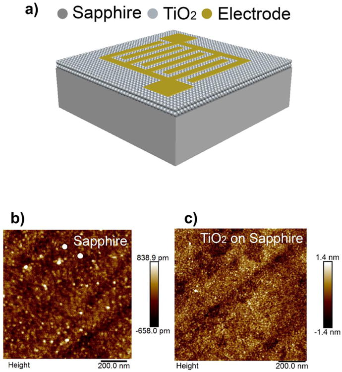
Fabricated TiO2 thin-film device: (a) Schematic of the device showing TiO2 along with sapphire substrate and Ti/Al/Ti/Au contacts. AFM images of (b) sapphire substrate and (c) TiO2 coated sample after annealing at 700 °C in Ar ambient for 30 s.
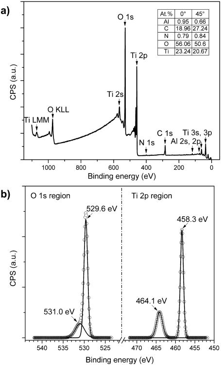
Fig. 2a shows a full spectrum XPS survey scan of a prepared TiO2/sapphire sample collected at 0° to the surface normal. The peak intensities are normalized by the Kratos relative sensitivity factors provided by CasaXPS. The inset of Fig. 2a lists the surface compositions with the uncertainties due to spectrum fitting. A 5% uncertainty is estimated for measurement reproducibility (data not shown). The compositions are calculated from XPS survey scans collected at both 0° and 45° to the surface normal. All peaks in the spectrum are attributed to the sputter-deposited TiO2 or the sapphire substrate except for C and negligible amount of N. The relative increase in C atomic percentage observed at 45° indicates that the species arises from the surface contamination, presumably due to exposure of the sample to the ambient environment after deposition. Fig. 2b shows high resolution, deconvoluted XPS scans of the Ti 2p and O 1s regions. A typical Ti 2p doublet peaks centered at 458.3 eV and 464.1 eV verifies the presence of TiO2 (Ti4+) while the main O 1s peak at 529.6 eV is assigned to lattice oxygen from TiO2, and the side peak at higher binding energy is attributed to surface hydroxylation [20, 21].
Figure 2.
XPS spectra of the prepared TiO2 thin-film: (a) Full spectrum survey scan collected at 0° to the surface normal. The inset shows the calculated surface compositions from XPS survey scans performed at both 0° and 45° to the surface normal. (b) High resolution scans of O 1s and Ti 2p regions with background signal removals. The solid lines represent the deconvoluted peaks from collected signals (denoted by open circles). The binding energy scales of all spectra are calibrated to the C 1s C*-C peak at 284.5 eV.
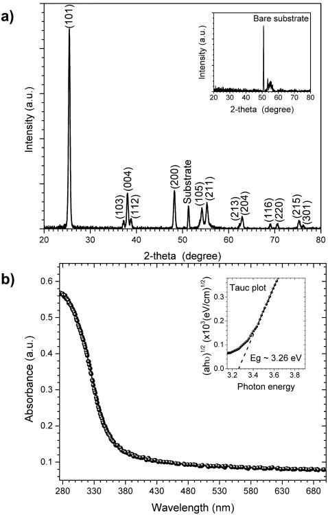
Fig. 3a shows XRD patterns of the prepared 50 nm TiO2 film on a 3-inch Si substrate. We use the large Si substrate instead of small sapphire pieces as large surface area of TiO2 yields better signal-to-noise ratio in our XRD measurement. Results by other groups show that for rf-sputtered TiO2, the nature of substrate has very limited influence on the crystal structure of the deposited film [22]. The inset shows the XRD diffraction peaks obtained from a bare substrate. All the diffraction peaks in Fig. 3a are assigned to the anatase phase. No rutile phase is observed in the XRD patterns. Thus, the XRD data indicates that the prepared TiO2 film is a polycrystalline anatase phase, which is likely due to the low deposition temperature (< 400 °C) [23] and the low annealing temperature (< 900 °C) [24]. Fig. 3b shows the UV-vis absorbance of the prepared TiO2 film in the 275 nm to 700 nm wavelength range. A sharp decrease of the film absorbance in the visible region (λ > 400 nm) shows a high transparency of the film in the visible region.
Figure 3.
(a) XRD patterns of 50 nm TiO2 coated Si showing diffraction peaks arising exclusively from anatase phase of prepared TiO2 and Si substrate. The inset confirms the diffraction peaks of the Si substrate. (b) Obtained absorbance spectrum of the prepared TiO2 thin-film from UV to visible light regions. The inset shows the estimation of the indirect optical band gap of TiO2 using Tauc plot.
The inset of Fig. 3b shows the Tauc plot which relates the absorption coefficient α to photon energy hν. In general, the absorption coefficient obeys the following empirical relation [25]:
where β-1 is the band edge parameter, Eg is the band-gap energy, and r is a number that denotes the nature of electronic transition. For allowed indirect transitions, which is the case for TiO2, r is 2 [26]. By following Tauc's approach, the optical band-gap energy Eg is determined by extrapolating the linear region of the plot of (αhν)1/2 versus hν to hν = 0. Therefore, the estimated optical bandgap of the prepared TiO2 is 3.26 eV, in good agreement with reported anatase values [23].
Sensing performance
Fig. 4a shows the room-temperature dynamic responses of the TiO2 sensors exposed to 250 ppm NO2 under UV illumination and in dark conditions. For both UV on and off conditions, the sensors are subjected to 250 ppm NO2 exposure for 5 min followed by 5 min exposure to breathing air. Under UV illumination, the current level of the sensor increases roughly 5.5 times over the dark condition. Compared to the small and noisy gas response in the dark, the sensor demonstrates reversible and distinct NO2 chemiresistive response under UV illumination. Moreover, unlike shifting of the baseline current observed in the dark operation, the TiO2 sensor maintains constant baseline current after three gas exposure cycles under UV illumination. Notably, this stable baseline current is essential for sensing applications. The response of the TiO2 sensor is defined as the relative change in resistance in presence of the analyte,
Figure 4.
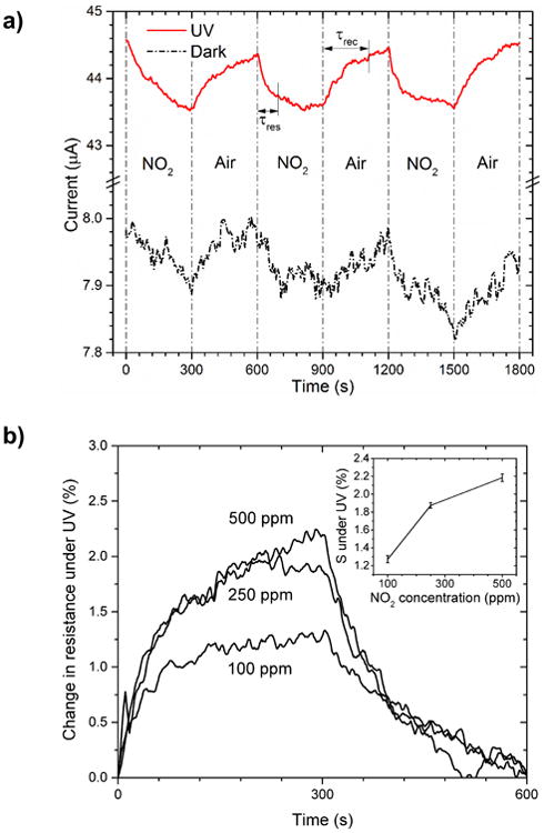
Dynamic responses of the TiO2 based sensor exposed to: (a) 250 ppm NO2 mixed with breathing air under UV illumination and dark. (b) Comparison of NO2 response under UV at mixture of 100 ppm, 250 ppm, and 500 ppm with breathing air. The inset shows the measured responses under UV as a function of NO2 concentrations with uncertainty.
where Rg and Ro are measured resistances of the sensor with NO2 and air flow, respectively. The calculated responses with and without UV illumination are 2.4% and 1.6%, respectively. When exposed to NO2, the response time (τres) is defined as the time taken by the sensor current to reach 80% of the response (I0 - If), where I0 stands for the current measured in air and If is the steady current in the presence of the analyte. While the recovery time (τrec) represents the time required for the sensor to recover to 20% of the response with air flow. The τres = 100 s and τrec = 210 s are observed for sensing operation under UV as marked in Fig. 4a. Due to the noisy signal, the corresponding response and recovery time for the dark case are difficult to estimate accurately.
Fig. 4b shows the responses of the sensor to different NO2 concentrations under UV illumination at room-temperature. The response is tested for NO2 concentrations ranging from 100 ppm to 500 ppm. The response reaches saturation at high concentration under UV illumination. Such wide sensing range makes the TiO2 film suitable for industrial NO2 sensor applications.
Mechanism of NO2 sensing under UV
A proposed possible gas sensing mechanism of the TiO2 based sensor is illustrated in Fig. 5. According to surface science experiment results, oxygen adsorbs on TiO2 surface at a broad range of temperature from 105 K to 1000 K [27, 28]. The adsorbed oxygen are chemisorbed at oxygen vacancy sites, surrounded by Ti3+ pairs, forming oxygen anions on TiO2 surface [29]. Meanwhile, reports have confirmed as the dominant chemisorbed species on TiO2 [28, 30]. Therefore, the adsorption of the oxygen is equivalent to the ionosorption of oxygen by taking nearby electrons near on TiO2 surface as described by the following equation [17],
Figure 5.
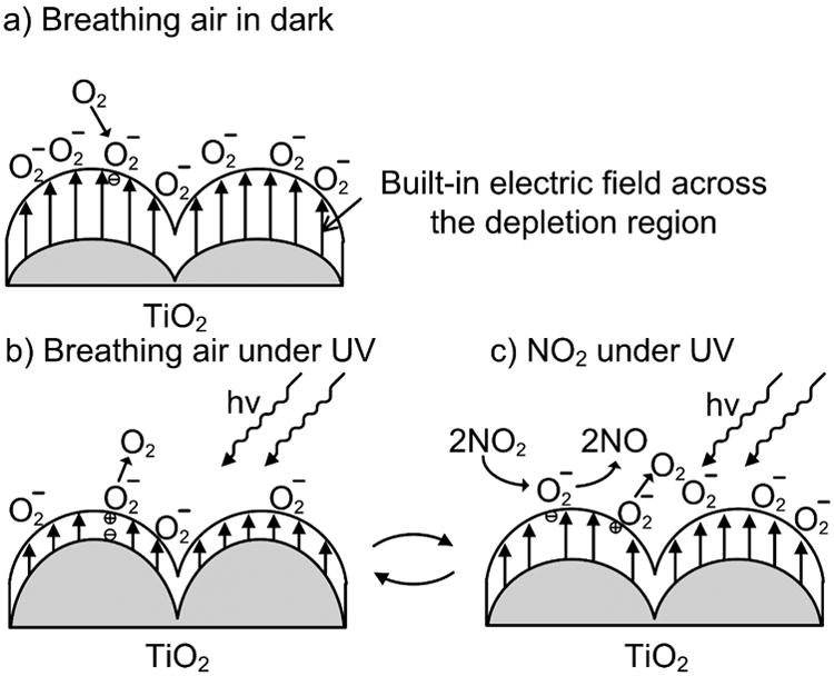
Schematic of proposed NO2 gas sensing mechanism of the TiO2 sensor under UV illumination: (a) In dark environment with breathing air in. (b) Under UV illumination in breathing air. (c) Under UV illumination with mixture of NO2 and breathing air.
The schematic shown in Fig. 5a describes such a condition where is adsorbed on the polycrystalline TiO2 surface in dark. The surface-adsorbed induces the built-in electric field across the depletion region, resulting in high resistance in the dark. Upon UV illumination, photogenerated electron-hole pairs within the depletion region are separated by the electric filed. While photogenerated electrons are driven into the bulk, photogenerated holes migrate to the surface and recombine with the adsorbed . Both processes decrease the depth of the depletion region, leading to the increase in current. Eventually, the surface adsorption and desorption processes of oxygen reach equilibrium as depicted in Fig. 5b. When exposed to NO2 as shown in Fig. 5c, the resistance of the sensor increases due to the following reaction [31],
NO2 acts as a scavenger for photogenerated electron, resulting in decreasing the photo current. In addition, this reaction also restores surface adsorbed concentration, which broadens the depletion region, resulting in further decrease of the current. Table 1 summarizes some of the proposed NO2 sensors based on TiO2 and their corresponding operating conditions.
Table 1. Operation conditions of TiO2 based NO2 sensors.
| Sensor materials (dopant) | Operation temperature (°C) | Detection limits (ppm) |
|---|---|---|
| TiO2-WO3 [32] | 350-800 | 20 |
| ZnO-TiO2 [14] | 250 | 2-20 |
| TiO2 [10] | 450-550 | 2-25 |
| TiO2(Cr) [9] | 250 | 2-50 |
| TiO2(Al) [13] | 400-800 | 50-200 |
| Nano-tubular TiO2 [12] | 300-500 | 10-100 |
| Nano-tubular TiO2(Nb) [11] | 100-200 | 10 |
| TiO2 (this work) | Room-temperature, UV | 100-500 |
Conclusions
In this study, we have successfully fabricated selective TiO2 based NO2 sensors that work at room-temperature under UV illumination. The prepared anatase TiO2 thin-film exhibits small grain size, smooth surface, and sharp UV absorbance. Assisted by UV illumination, the TiO2 film shows a reversible and distinct NO2 response with a relatively short response time at room-temperature. No response to the CO or CO2 is measured with the TiO2 based sensors. The measured responses to different NO2 concentrations indicate a broad detecting range from 100 ppm to 500 ppm. The proposed gas sensing mechanism under UV relies on the modulation of the depletion region in TiO2 due to the change in surface-adsorbed oxygen concentration.
Acknowledgments
This work was sponsored through N5 Sensors and the Maryland Industrial Partnerships (MIPS, #5418). The TiO2 based NO2 gas sensing devices were fabricated in the Nanofab of the NIST Center for Nanoscale Science and Technology. Gas sensing measurements were conducted at N5 Sensors, Inc. The authors would like to acknowledge the technical support from Mr. Audie Castillo.
Footnotes
Certain commercial equipment, instruments, or materials are identified in this paper in order to specify the experimental procedure adequately. Such identification is not intended to imply recommendation or endorsement by the National Institute of Standards and Technology, nor is it intended to imply that the materials or equipment identified are necessarily the best available for the purpose.
References
- 1.Comini E, Faglia G, Sberveglieri G. UV light activation of tin oxide thin films for NO2 sensing at low temperatures. Sensors and Actuators B-Chemical. 2001;78:73–77. [Google Scholar]
- 2.Dai Z, Lee CS, Tian Y, Kim ID, Lee JH. Highly reversible switching from P- to N-type NO2 sensing in a monolayer Fe2O3 inverse opal film and the associated P-N transition phase diagram. Journal of Materials Chemistry A. 2015;3:3372–3381. [Google Scholar]
- 3.Yoo J, Yoon H, Wachsman ED. Sensing properties of MOx/YSZ/Pt (MOx = Cr2O3, SnO2, CeO2) potentiometric sensor for NO2 detection. J Electrochem Soc. 2006;153:H217–H221. [Google Scholar]
- 4.Das A, Dost R, Richardson T, Grell M, Morrison JJ, Turner ML. A nitrogen dioxide sensor based on an organic transistor constructed from amorphous semiconducting polymers. Advanced Materials. 2007;19:4018–4023. [Google Scholar]
- 5.Eranna G, Joshi BC, Runthala DP, Gupta RP. Oxide materials for development of integrated gas sensors - A comprehensive review. Critical Reviews in Solid State and Materials Sciences. 2004;29:111–188. [Google Scholar]
- 6.Williams DE. Semiconducting oxides as gas-sensitive resistors. Sensors and Actuators B-Chemical. 1999;57:1–16. [Google Scholar]
- 7.Debnath R, Xie T, Wen BM, Li W, Ha JY, Sullivan NF, Nguyen NV, Motayed A. A solution-processed high-efficiency p-NiO/n-ZnO heterojunction photodetector. RSC Advances. 2015;5:14646–14652. [Google Scholar]
- 8.Xie T, Liu G, Wen B, Ha JY, Nguyen NV, Motayed A, Debnath R. Tunable Ultraviolet Photoresponse in Solution-Processed p–n Junction Photodiodes Based on Transition-Metal Oxides. ACS Applied Materials & Interfaces. 2015;7:9660–9667. doi: 10.1021/acsami.5b01420. [DOI] [PubMed] [Google Scholar]
- 9.Ruiz AM, Sakai G, Cornet A, Shimanoe K, Morante JR, Yamazoe N. Cr-doped TiO2 gas sensor for exhaust NO2 monitoring. Sensors and Actuators B-Chemical. 2003;93:509–518. [Google Scholar]
- 10.Esmaeilzadeh J, Marzbanrad E, Zamani C, Raissi B. Fabrication of undoped-TiO2 nanostructure-based NO2 high temperature gas sensor using low frequency AC electrophoretic deposition method. Sensors and Actuators B-Chemical. 2012;161:401–405. [Google Scholar]
- 11.Galstyan V, Comini E, Faglia G, Vomiero A, Borgese L, Bontempi E, Sberveglieri G. Fabrication and investigation of gas sensing properties of Nb-doped TiO2 nanotubular arrays. Nanotechnology. 2012;23:235706. doi: 10.1088/0957-4484/23/23/235706. [DOI] [PubMed] [Google Scholar]
- 12.Gonullu Y, Rodriguez GCM, Saruhan B, Urgen M. Improvement of gas sensing performance of TiO2 towards NO2 by nano-tubular structuring. Sensors and Actuators B-Chemical. 2012;169:151–160. [Google Scholar]
- 13.Saruhan B, Yuce A, Gonullu Y, Kelm K. Effect of Al doping on NO2 gas sensing of TiO2 at elevated temperatures. Sensors and Actuators B-Chemical. 2013;187:586–597. [Google Scholar]
- 14.Vyas R, Sharma S, Gupta P, Vijay YK, Prasad AK, Tyagi AK, Sachdev K, Sharma SK. Enhanced NO2 sensing using ZnO-TiO2 nanocomposite thin films. Journal of Alloys and Compounds. 2013;554:59–63. [Google Scholar]
- 15.Haridas D, Gupta V. Study of collective efforts of catalytic activity and photoactivation to enhance room temperature response of SnO2 thin film sensor for methane. Sensors and Actuators B-Chemical. 2013;182:741–746. [Google Scholar]
- 16.Comini E, Cristalli A, Faglia G, Sberveglieri G. Light enhanced gas sensing properties of indium oxide and tin dioxide sensors. Sensors and Actuators B-Chemical. 2000;65:260–263. [Google Scholar]
- 17.Chen H, Liu Y, Xie CS, Wu J, Zeng DW, Liao YC. A comparative study on UV light activated porous TiO2 and ZnO film sensors for gas sensing at room temperature. Ceramics International. 2012;38:503–509. [Google Scholar]
- 18.Dhivya P, Prasad AK, Sridharan M. Nanostructured TiO2 films: Enhanced NH3 detection at room temperature. Ceramics International. 2014;40:409–415. [Google Scholar]
- 19.Mardare D, Tasca M, Delibas M, Rusu GI. On the structural properties and optical transmittance of TiO2 r.f. sputtered thin films. Applied Surface Science. 2000;156:200–206. [Google Scholar]
- 20.McCafferty E, Wightman JP. Determination of the concentration of surface hydroxyl groups on metal oxide films by a quantitative XPS method. Surface and Interface Analysis. 1998;26:549–564. [Google Scholar]
- 21.Trimboli J, Mottern M, Verweij H, Dutta PK. Interaction of water with titania: Implications for high-temperature gas sensing. Journal of Physical Chemistry B. 2006;110:5647–5654. doi: 10.1021/jp0551519. [DOI] [PubMed] [Google Scholar]
- 22.Al-Homoudi IA, Thakur JS, Naik R, Auner GW, Newaz G. Anatase TiO2 films based CO gas sensor: Film thickness, substrate and temperature effects. Applied Surface Science. 2007;253:8607–8614. [Google Scholar]
- 23.Tang H, Prasad K, Sanjines R, Schmid PE, Levy F. Electrical and optical properties of TiO2 anatase thin-films. Journal of Applied Physics. 1994;75:2042–2047. [Google Scholar]
- 24.Hou YQ, Zhuang DM, Zhang G, Zhao M, Wu MS. Influence of annealing temperature on the properties of titanium oxide thin film. Applied Surface Science. 2003;218:97–105. [Google Scholar]
- 25.Urbach F. The long-wavelength edge of photographic sensitivity and of the electronic absorption of solids Physical Review. 1953;92:1324–1324. [Google Scholar]
- 26.Tauc J, Grigorov R, Vancu A. Optical properties and electronic structure of amorphous germanium. Physica Status Solidi. 1966;15:627–637. [Google Scholar]
- 27.Lu GQ, Linsebigler A, Yates JT. The adsorption and photodesorption of oxygen on the TiO2(110) surface. Journal of Chemical Physics. 1995;102:4657–4662. [Google Scholar]
- 28.Gopel W, Rocker G, Feierabend R. Intrinsic defects of TiO2(110): Interaction with chemisorbed O2, H2, CO, and CO2. Physical Review B. 1983;28:3427–3438. [Google Scholar]
- 29.Shu C, Sukumar N, Ursenbach CP. Adsorption of O2 on TiO2(110): A theoretical study. Journal of Chemical Physics. 1999;110:10539–10544. [Google Scholar]
- 30.Naccache C, Meriaude P, Che M, Tench AJ. Identification of oxygen species adsorbed on reduced titanium dioxide. Transactions of the Faraday Society. 1971;67:506–512. [Google Scholar]
- 31.Lu GY, Xu J, Sun JB, Yu YS, Zhang YQ, Liu FM. UV-enhanced room temperature NO2 sensor using ZnO nanorods modified with SnO2 nanoparticles. Sensors and Actuators B-Chemical. 2012;162:82–88. [Google Scholar]
- 32.Guidi V, Carotta MC, Ferroni M, Martinelli G, Paglialonga L, Comini E, Sberveglieri G. Preparation of nanosized titania thick and thin films as gas-sensors. Sensors and Actuators B-Chemical. 1999;57:197–200. [Google Scholar]


