Significance
The ability to electrically control collective electron states is a central goal of materials research and may allow for the development of novel devices. 1T-TaS2 is an ideal candidate for such devices due to the existence of various charge ordered states in its phase diagram. Although various techniques have been demonstrated to manipulate charge order in 1T-TaS2, a fundamental understanding of the effects is still lacking, and the methods used are incompatible with device fabrication. By using both high-resolution transmission electron microscopy and electronic transport to investigate atomically thin 1T-TaS2 samples, we clarify the microscopic nature of the charge ordered phases in the 2D limit and further control them by all-electrical means.
Keywords: two-dimensional materials, strongly correlated systems, charge density waves
Abstract
The layered transition metal dichalcogenides host a rich collection of charge density wave phases in which both the conduction electrons and the atomic structure display translational symmetry breaking. Manipulating these complex states by purely electronic methods has been a long-sought scientific and technological goal. Here, we show how this can be achieved in 1T-TaS2 in the 2D limit. We first demonstrate that the intrinsic properties of atomically thin flakes are preserved by encapsulation with hexagonal boron nitride in inert atmosphere. We use this facile assembly method together with transmission electron microscopy and transport measurements to probe the nature of the 2D state and show that its conductance is dominated by discommensurations. The discommensuration structure can be precisely tuned in few-layer samples by an in-plane electric current, allowing continuous electrical control over the discommensuration-melting transition in 2D.
Layered 1T-TaS2 exhibits a number of unique structural and electronic phases. At low temperature and ambient pressure, the ground state is a commensurate (C) charge density wave (CDW). On heating, it undergoes a sequence of first-order phase transitions to a nearly commensurate (NC) CDW at 225 K, to an incommensurate (IC) CDW at 355 K, and finally to a metallic phase at 545 K. Each transition involves both conduction electron and lattice degrees of freedom—large changes in electronic transport properties occur, concomitant with structural changes to the crystal. By either chemical doping or applying high pressures, it is possible to suppress the CDWs and induce superconductivity (1–3). For device applications, it is desirable to control these phases by electrical means, but this capability is difficult to achieve in bulk crystals due to the high conduction electron density. Recent efforts to produce thin samples by mechanical exfoliation provide a new avenue for manipulating the CDWs in 1T-TaS2 (4–8). These studies have demonstrated the suppression of CDW phase transitions using polar electrolytes, as well as resistive switching between the different phases. As the material approaches the 2D limit, however, significant changes have been observed in the transport properties (4, 5, 8). However, the microscopic nature of the 2D state remains unclear. In this work, we use transmission electron microscopy (TEM) together with transport measurements to develop a systematic understanding of the CDW phases and phase transitions in ultrathin 1T-TaS2. We find that charge ordering disappears in flakes with few atomic layers due to surface oxidation. When samples are instead environmentally protected, the CDWs persist and their transitions can be carefully tuned by electric currents.
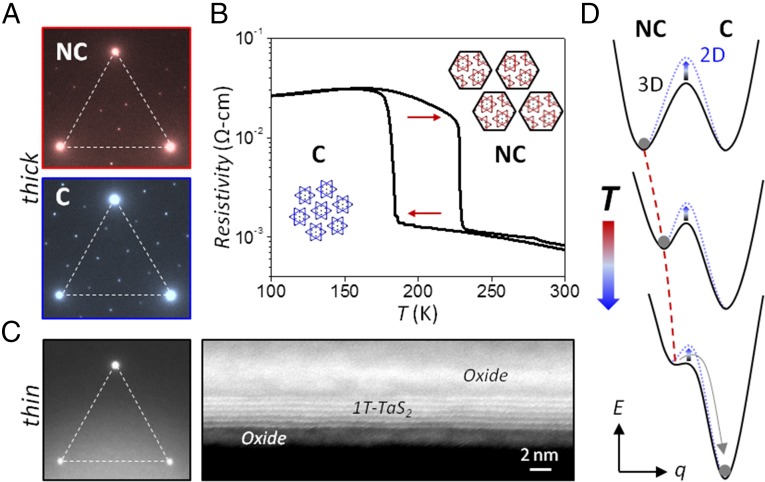
Both the atomic and CDW structure of 1T-TaS2 can be visualized in reciprocal space by TEM electron diffraction (9, 10). In Fig. 1A, we show diffraction images taken from a bulk-like, 50-nm-thick crystal at low and room temperature (C phase, blue panel; NC phase, red panel). The bright peaks (connected by dashed lines) correspond to Bragg scattering from a triangular lattice of Ta atoms with lattice constant a = 3.36 Å. Additional weaker diffraction peaks appear from the periodic atomic displacements of the CDW. In the low-temperature C phase, Ta atoms displace to make Star-of-David clusters (blue inset, Fig. 1B). The outer 12 atoms within each star displace slightly inward toward the atom at the center, giving rise to a commensurate superstructure with wavelength λC = a that is rotated ϕC = 13.9° with respect to the atomic lattice. The NC phase at room temperature also consists of such 13-atom distortions. Scanning tunneling microscope (STM) measurements have revealed, however, that such ordering is only preserved in quasi-hexagonal domains consisting of tens of stars (11, 12), with domain periodicity 60–90 Å depending on temperature (13, 14). The domains are separated by a discommensuration network forming a Kagome lattice, inside of which the Ta displacements are substantially reduced (15). A schematic of this structure is shown in the red inset of Fig. 1B.
Fig. 1.
NC-C CDW phase transition in bulk 1T-TaS2 and CDW suppression by oxidation in thin flakes. (A) TEM diffraction images of 50-nm-thick 1T-TaS2 at 295 K (red, NC phase) and 100 K (blue, C phase). Weaker peaks are due to CDW distortion. (B) Resistivity vs. temperature of bulk 1T-TaS2 crystal around the first-order, NC-C transition. (Insets) Real space schematics of CDW structure. (C) (Left) TEM diffraction of few-layer 1T-TaS2 flake shows absence of CDW order. (Right) High-resolution, cross section electron microscopy image reveals presence of amorphous oxide. (D) Free energy schematic of CDW evolution with temperature. Vertical and horizontal axis represent free energy (E) and reaction coordinate (q), respectively. NC domains grow slowly upon cooling until abrupt transition into the C phase. Energy barrier increases in 2D samples protected from oxidation.
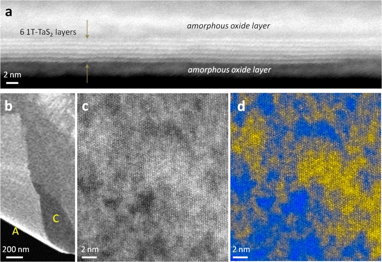
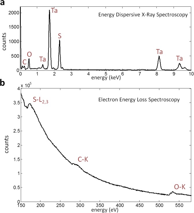
When ultrathin 1T-TaS2 crystals (approximately <5 nm thickness) are exfoliated in an ambient air environment, the CDW structure is not observed by the TEM electron diffraction. In the left panel of Fig. 1C, we show a room temperature electron diffraction pattern taken on a few-layer flake. The presence of Bragg peaks without CDW scattering suggests that the 1T-TaS2 layers are in a phase that is not observed in bulk crystals at this temperature. High-resolution electron microscopy and energy dispersive spectroscopy on fully suspended samples reveal a strong presence of oxidation as well as an amorphous layer on the surface (Figs. S1 and S2). The amorphous oxide (∼2 nm thickness) can be clearly seen atop both surfaces of the 1T-TaS2 layers in cross section (Fig. 1C, Right). It is possible that oxidation leads to strong surface pinning, which destroys charge ordering in ultrathin samples. Recent resistivity measurements on exfoliated 1T-TaS2 crystals have also reported the disappearance of CDWs in sufficiently thin flakes (5). It is not clear, however, whether these are intrinsic effects related to dimensionality or extrinsic consequences of oxidation.
Fig. S1.
High-resolution STEM image of ultrathin 1T-TaS2 prepared in air. (A) Amorphous layers appear on the top and bottom surfaces. (B) Overview of a curled sheet providing in-plane (A) and planar (C) and viewing. (C) High-resolution STEM image of the 1T-TaS2 sheet shows the high-frequency atomic structure and a lower frequency intensity variation corresponding to the amorphous surface layers. The amorphous surfaces are more clearly visualized in D, which uses Lab Color space to create blue/yellow contrast of the amorphous (low-frequency) intensity variation.
Fig. S2.
Chemical analysis with STEM-spectroscopy of ultrathin 1T-TaS2 exfoliated in air. In addition to the expected presence of Ta and S, oxygen and trace amounts of carbon are present in both the (A) dispersive X-ray and (B) electron energy loss spectroscopy. The sample was suspended such that all detected elements represent chemical species present in the specimen.
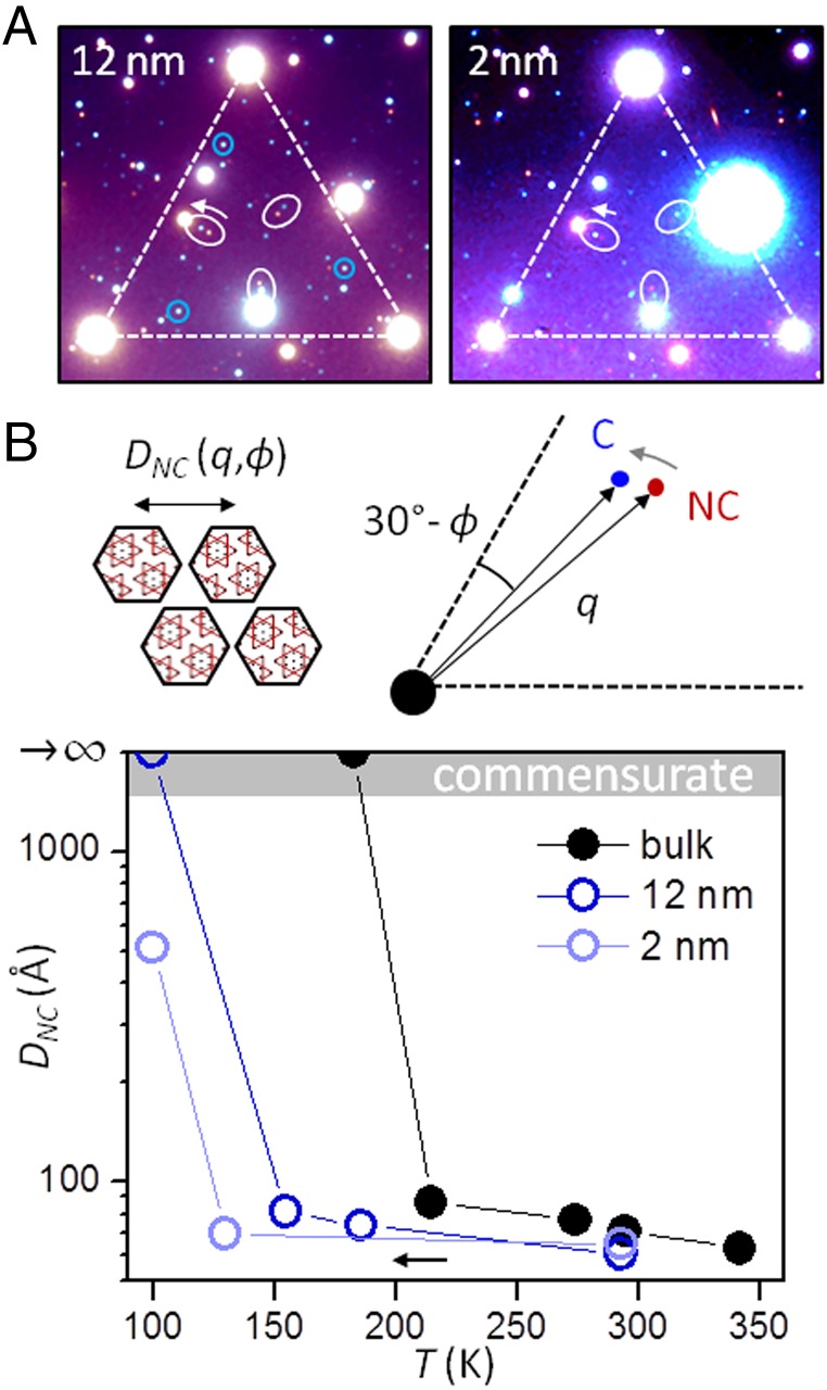
To prevent surface oxidation, we exfoliated 1T-TaS2 crystals within a nitrogen-filled glove box with under 2-ppm oxygen concentration. The flakes were protected by a capping layer of thin hexagonal boron nitride (hBN) before transfer out into the ambient environment (Methods). TEM diffraction performed on these protected samples reveals that CDW formation persists down to the lowest thicknesses measured (2 nm), as we discuss in detail in Fig. 4. This finding indicates that the absence of charge order in ultrathin, uncovered flakes is most likely caused by the effects of oxidation. The study and utilization of CDWs in 2D 1T-TaS2 thus requires careful sample preparation in inert atmosphere.
Fig. 4.
Dimensional dependence of phase transition—electron diffraction. (A) Overlaid TEM diffraction images of ultrathin 1T-TaS2 covered with hBN taken at 295 K (red peaks) and 100 K (blue peaks) for two flake thicknesses. hBN preserves CDW order (circled peaks) but introduces additional diffraction spots. (B) (Upper Right) Zoom-in schematic of CDW diffraction peaks showing temperature evolution. Position of NC spot can be used to estimate commensurate domain periodicity DNC (Upper Left). (Lower) DNC vs. temperature with cooling measured for the two covered samples compared with data reproduced from ref. 14. Reduced thickness pushes NC to C phase transition to lower temperature.
The different structural phases of 1T-TaS2 exhibit distinct electronic transport properties that may be exploited for device applications. In the main panel of Fig. 1B, we show temperature-dependent resistivity of a bulk crystal measured across the NC-C phase transition. Resistivity abruptly increases (decreases) by over an order of magnitude on entering the C (NC) phase. The hysteresis loop between cooling and warming defines the temperature region of metastability between the two phases and can be understood by a free energy picture (Fig. 1D). In a first-order transition, an activation barrier separates the stable energy minima corresponding to the NC and C states. With cooling from the NC phase, both the C state energy and the height of the barrier decrease with respect to the NC energy. When the C state has lower energy, the NC phase becomes metastable, but the system only transitions into the C phase when the activation barrier becomes comparable to the thermal energy. The situation is reversed when warming from the C phase. In oxidation-free 2D samples, this electronic transition is qualitatively unchanged.
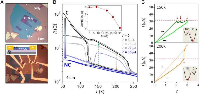
Fig. 2A shows an example of hBN-encapsulated 1T-TaS2 flakes before (Upper) and after device fabrication (Lower). To make electrical contact to the covered samples, we used a technique of edge metallization developed for graphene/hBN heterostructures (Methods) (16). A side-view device schematic is shown in the Inset of the lower panel. In the main panel of Fig. 2B (I = 0, black curve), we plot resistance as a function of temperature for a 4-nm-thick sample measured across the NC-C phase transition. The behavior is similar to that of the bulk crystal (Fig. 1B); however, the hysteretic region between cooling and warming is substantially widened, indicating that one or both of the CDW phases become more metastable.
Fig. 2.
Electrical control of NC-C transition in oxidation-free, 2D devices. (A) Optical images of 1T-TaS2 flakes on a SiO2/Si wafer covered by hBN in inert atmosphere before (Upper) and after (Lower) side electrical contact. (Inset) Side-view device schematic. (B) ac resistance vs. temperature for 4-nm-thick device as a function of dc current. Continuous current flow stabilizes NC phase at low temperature. Normalized resistance difference between cooling and warming is plotted as a function of dc current in Inset. (C) (Upper) Current vs. voltage sweep at 150 K starting in NC phase shows abrupt decreases in current and transition to the C phase. (Lower) Same at 200 K starting in C phase shows abrupt increase in current and transition to NC phase. Sweep rate is 3–6 V/min. Free energy schematics of electrically induced transitions are plotted in Insets.
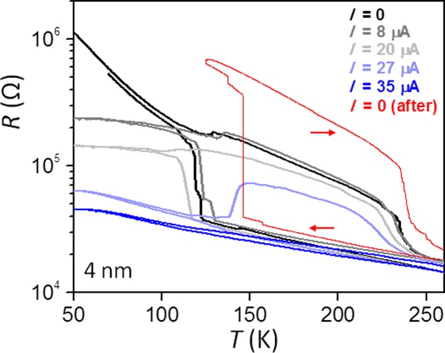
Metastable phases of a CDW system are generally more susceptible to electronic perturbations, because CDWs directly couple to electric field (6–8, 17). In our device, we observe that continuous current flow stabilizes the NC phase at low temperatures. In Fig. 2B (main panel), we show ac resistance with temperature while also applying a continuous, in-plane dc current, starting at room temperature (300 K). As the dc current I is increased, the final resistance at low temperature is monotonically lowered. Concomitant with this trend, the resistance jump resulting from the NC-C phase transition also decreases with increasing I. In the Inset, we plotted the ratio of the resistance difference between cooling and warming, ∆R, to resistance R in the more conducting state at T = 180 K, the temperature in the middle of the hysteresis region, as a function of the dc current level. For I = 35 μA (blue curve in main panel), the NC-C phase transition is completely absent. This measurement indicates that C phase formation in the current driven sample is very different compared with the zero-current, equilibrium condition. Current flow hinders the formation of the C phase and maintains the sample in the more conductive NC state at low temperature. We exclude Joule heating of the sample as a possible explanation by slowly turning off the current at low temperature and verifying that the resistance does not change. We also note that cooling and warming the sample again without dc current flow reproduces the original phase transitions (Fig. S3), indicating that the currents have not damaged the flake irreversibly.
Fig. S3.
Resistance vs. temperature before and after dc current measurements. Trace for I = 0 (after) reproduces original phase transitions suppressed by large dc current.
Our observation suggests that it is possible to maintain the NC phase in a temperature region where it is not thermodynamically stable. We now show that the opposite phenomenon is also possible, i.e., we can drive a transition toward the thermodynamically stable state, if we apply an in-plane current after cooling or warming the sample in equilibrium. Fig. 2C shows the current induced phase transitions in the same device (4 nm thickness). Here, we start in the NC phase at room temperature and cool the sample down to 150 K without current flow. At this temperature, although the sample remains in the NC state, the NC phase is now metastable, and the C phase is the thermodynamically stable state. As we increase the voltage across the device (upper panel, dark green curve), the measured current through the device decreases in abrupt steps (marked by red arrows) when it reaches a critical current Ic ∼ 30 μA (marked by red dashed line). On sweeping the bias current back to zero (light green curve), the device remains in a more insulating state. Warming up the sample after this point produces a temperature curve similar to the C phase, and a transition to the NC phase is observed. We have demonstrated that a bias current applied to the sample can be used to drive the metastable NC phase toward the thermodynamically preferred C state. The dashed green arrow in Fig. 2B marks the direction of this current-induced NC to C phase transition and a free energy schematic of this process is shown in the Inset of the upper panel of Fig. 2C.
Similarly, the metastable C state can also be driven toward the NC phase with current. Here, we start in the C phase at 50 K and warm up to 200 K. The sample remains in the C phase, but now the NC phase is the thermodynamic ground state. As shown in the lower panel of Fig. 2C, sweeping the voltage in this case results in a sharp increase in current and drives the sample toward the more conducting NC state. We have used the dashed orange arrow in Fig. 2B and the free energy picture in the inset of the lower panel of Fig. 2C to represent this opposite C to NC transition. Interestingly, both induced transitions occur when the current reaches about Ic ∼ 30 μA, indicating that indeed current flow rather than electric field is the underlying mechanism that drives the transition. We repeated this measurement at various temperatures and initial conditions. In all cases, whenever the initial system is metastable, reaching a current threshold of 30 to 40 μA drives the system toward the thermodynamically stable state, regardless of device resistance. In contrast, we observe no induced transition up to 45 μA at 260 K, where a metastable phase ceases to exist.
Taken together, the results of Fig. 2 demonstrate that it is possible to electrically control the NC-C transition in 2D 1T-TaS2, where the temperature region of metastability is significantly enhanced. A more detailed study of this phase transition in 2D samples, however, can provide a better understanding of our experimental observations. The key structural difference between the two CDW phases is the presence of the discommensuration network in the NC phase (Fig. 1B, red inset). The NC-C transition can then be interpreted as a discommensuration-melting transition, which can be significantly affected by dimensionality (18, 19). The discommensurations have a striking effect on the electronic transport properties in 1T-TaS2. The NC phase is an order of magnitude more conductive than the C phase. If we assume that the interior of each commensurate domain has similar transport properties as the C phase, this then implies the discommensuration regions in the NC phase are at least 10 times more conductive than the domain interior (3). Such a view is supported by the fact that the atomic structure within the discommensurations is close to the high-temperature metallic phase (15). With this interpretation, we can use transport measurements to better understand the role of dimensionality on the discommensuration-melting transition.
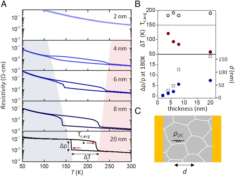
As the number of 1T-TaS2 layers decreases, the resistivity change corresponding to the NC-C phase transition evolves in a continuous manner down to 2 nm thickness in environmentally protected samples. Fig. 3A shows resistivity as a function of temperature for four hBN-covered 1T-TaS2 flakes, all measured using a 1 K/min sweep rate. Their thicknesses are 2, 4, 6, and 8 nm as determined using an atomic force microscope. For comparison, we show data from an unprotected, 20-nm-thick flake, which exhibits characteristics similar to the bulk crystal, indicating that the effects of oxidation are less pronounced in thicker samples. The temperature hysteresis associated with the phase transition between cooling and warming is substantially increased in thinner samples, consistent with our earlier observations of the device in Fig. 2A. The progressive widening of the hysteresis loop continues down to the 4-nm-thick device, below which there is no longer a detectable transition. A guide to the eye for the expansion of this metastable region is shown by the colors in Fig. 3A. In the upper panel of Fig. 3B, we plot ∆T = Tc,warm – Tc,cool as a function of flake thickness, where Tc,warm and Tc,cool are the experimentally observed NC to C or C to NC transition temperature during the warming or cooling process, respectively. Here, Tc is determined by the temperature at which the first derivative peaks in the temperature sweep. ∆T is 60 K for the 20-nm flake, slightly larger than that for the bulk crystal (40 K), and grows to 120 K for the 4-nm device. In the same panel, we also plot the average temperature Tc,avg = (Tc,warm + Tc,cool)/2 of the transition. Tc,avg does not change substantially with thickness and remains between 180 and 190 K, which then implies that lower dimensionality does not stabilize either the NC or C phase. Instead, the NC (C) phase becomes increasingly metastable during cooling (warming) for thinner samples, indicating that the size of the energy barrier separating the NC and C phases increases (Fig. 1D).
Fig. 3.
Dimensional dependence of phase transition—electron transport. (A) Thickness evolution of temperature-dependent resistivity around NC-C phase transition measured on hBN-covered ultrathin samples and 20-nm-thick flake. (B) Average transition temperature and temperature hysteresis (Upper) and normalized resistivity difference (Lower) between cooling and warming as a function of sample thickness. Open squares are corrections from contact resistance (Fig. S4). Hysteresis widens and resistivity difference decreases in thinner samples, whereas average transition temperature remains constant. Resistivity change can be used to estimate the discommensuration density 1/d at low temperature. (C) Circuit model of discommensuration network.
Although ∆T increases when sample thickness is reduced, the resistivity jump associated with the phase transition decreases with decreasing thickness. In the bottom panel of Fig. 3B, we plot the resistivity difference ∆ρ between cooling and warming at T = 180 K, normalized to ρ in the more conducting state as a function of flake thickness. The closed circles are extracted directly from the data in Fig. 3A, whereas the open squares are corrections due to the effects of contact resistance (Fig. S4). For the 20-nm device, resistivity changes by an order of magnitude. The change is smaller for thinner devices and disappears completely for the 2-nm device, which indicates that more conducting NC discommensurations persist at low temperatures for thinner samples, consistent with the larger energy barriers required to remove them. Also, the resistivity jump becomes less abrupt, which is a reflection that the phase transition has slowed, as larger energy barriers generally act also to impede the kinetics of a phase transition. A simple circuit model presented in Fig. 3C allows us to connect the measured resistance jump in the NC-C transition, ∆R, with the estimated density of discommensurations 1/d left in the low temperature phase. We assume that the device resistance at low temperature is dominated by conduction through a random network of discommensuration channels (shown as white lines), which is generally sensitive to the particular microstructure formed. However, for device sizes much larger than d, we find the resistance with discommensuration channels would be R ∼ ρDC d, where ρDC is the resistivity per unit length of each discommensuration channel. Similarly, in the high temperature NC phase with a well-defined discommensuration network, we have RNC ∼ ρDC DNC, where we assume DNC ∼ 80 Å (13, 14). From this, we can use the resistivity change in Fig. 3B to determine d: . On the right axis, we plotted d extracted for the different sample thicknesses. For the 2-nm sample, d ∼ DNC, whereas it grows to 70–160 nm for the 20-nm sample.
Fig. S4.
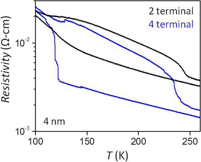
Extracting contact resistivity. Two- and four-terminal resistivity vs. temperature for 4-nm-thick flakes. The difference is proportional to resistivity of edge contacts.
We can further substantiate the microscopic picture presented above by providing atomic structural analysis based on TEM. As before, the CDW structure is preserved by environmentally controlled hBN encapsulation. In Fig. 4A, we show diffraction images taken from two 1T-TaS2 flakes of different thicknesses (12 and 2 nm). To highlight their temperature dependence, we have overlaid the diffraction patterns for each flake at 295 K (red peaks) and 100 K (blue peaks), our lowest achievable temperature. Ta Bragg peaks are again connected by a dashed triangle. Multiple scattering from hBN creates additional discernable peaks. The CDW peaks have been circled for easy identification. Although the peaks circled in gray appear qualitatively similar for both flakes, only the thicker flake displays additional peaks (circled in blue) at 100 K, indicating that it makes the transition to the C phase (compare with blue panel in Fig. 1A), whereas the thinner flake remains in the NC phase. This observation is consistent with our transport data as larger energy barriers in thinner samples require lower temperatures to realize the C phase.
The movement of the gray-circled peaks with cooling (denoted by arrows, Fig. 4A) can be understood more quantitatively with reference to the zoom-in schematic shown in Fig. 4B (Upper Right). The position of this CDW peak is related to the periodicity DNC of the NC domains (Upper Left) by a simple geometric expression (14): , where ∆ϕ is the difference in degrees between ϕ and ϕC = 13.9°, and ∆λ is the difference between the apparent wavelength averaged over many domains and λC = a. Thus, as the domain size grows, the NC peaks move closer to the C phase positions. We explicitly measured the position and angle of the CDW wave vectors for these two samples at several different temperatures during cooling to determine the domain period DNC using the expression above. The results are plotted in the lower panel of Fig. 4B. For comparison, we also reproduce STM results obtained by Thomson et al. on the surface of a bulk crystal (14). For bulk samples, DNC grows steadily from 60 to 90 Å on cooling from 340 to 215 K and then jumps to an arbitrarily large value on transition into the C phase at ∼180 K. At the same time, the width of the discommensuration regions remains relatively constant (∼22 Å) in all of the NC phase (13). As with our transport results, we find that reducing sample thickness suppresses the NC to C phase transition to lower temperatures during cooling and slows the CDW domain growth rate during the transition. For both of the thin flakes, the initial domain size at room temperature is similar to that that of the bulk crystal (DNC = 60–70 Å). DNC increases slightly upon cooling in the NC phase. For the 12-nm flake, the C phase is formed between 100 and 150 K, whereas the 2-nm flake remains in the NC phase even at 100 K. Its domain size here is much larger (DNC ∼ 500 Å), however, indicating that the phase transition has begun to take place. This result is in clear contrast to bulk samples where the transition is abrupt.
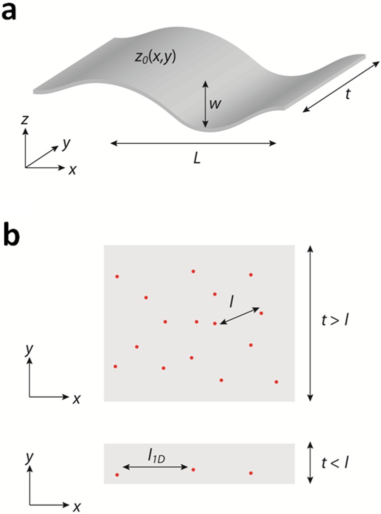
Our transport and TEM measurements both indicate that reduced dimensionality increases the energy barrier separating the NC and C CDW phases and thus widens the metastable region of the phase transition. The transition into the C phase involves melting or removal of the NC discommensuration network. Microscopically, energy barriers to discommensuration motion have been attributed to the presence of defects or impurities in the material, which act to pin them locally (20). Even in nominally pure CDW samples, clusters of localized defects have been observed by STM (21, 22), where the distance between defects is on the order of ∼10 nm. In bulk 1T-TaS2, the interlayer stacking of NC domains make the discommensuration walls extended planar objects (15, 23), which are generally more difficult to pin. In two dimensions, however, the discommensurations become lines, which may be more easily immobilized. We have constructed a model of discommensuration pinning for a 2D system of thickness t (Fig. S5). We find that in the ultrathin limit where t is smaller than the mean distance between impurities, the pinning energy for a discommensuration plane scales as Epin ∼ t−2/3, corresponding to a cross-over from collective weak pinning to strong individual pinning. These strong pinning centers stabilize the NC discommensuration network at low temperatures during cooling and will also hinder the nucleation and growth of discommensurations when warming from the C phase, thus increasing the temperature region of metastability for both CDW phases in accordance with our experimental observation.
Fig. S5.
Schematic picture of a DC plane and important length scales. A shows 3D view and B shows 2D projection. Red dots denote the location of impurities inside a dc plane. The effective mean impurity distance is l for t > l, whereas it is l1D for t < l.
By using this microscopic understanding of the NC-C phase transition in 2D samples, we may further elucidate the role of dc current in the measurements of Fig. 2 B and C. When the sample is cooled in equilibrium starting in the NC phase, the activation barrier between the NC and C states is continuously lowered, and therefore discommensurations are driven away and domain size grows steadily. Near the transition temperature, the small barrier can then be overcome with sufficient current flow, which depins the discommensurations to form the C phase ground state (Fig. 2C). On the other hand, when the sample is cooled out of equilibrium in the presence of a large dc current, it is likely that the domain size does not grow—the activation barrier remains large and the small-domain NC state persists on cooling to the lowest temperatures (Fig. 2B). The dc current is thus effectively a way to control the activation barrier between the NC and C phases.
Although a spatially resolved study is still needed to fully understand these effects, our results have both clarified the nature of the 2D state in 1T-TaS2 and demonstrated clear electrical control over the NC-C phase transition in ultrathin samples, further establishing the material’s relevance for device applications. We also expect our environmentally controlled techniques to be applicable for the study of other 2D transition-metal dichalcogenides that may be unstable under ambient conditions (24).
Methods
Synthesis of 1T-TaS2.
High-quality single crystals of 1T-TaS2 were grown by the chemical vapor transport (CVT) method with iodine as a transport agent. The high-purity Ta (3.5 N) and S (3.5 N) were mixed in chemical stoichiometry and heated at 850 °C for 4 d in an evacuated quartz tube. The harvested TaS2 powders and iodine (density: 5 mg/cm3) were then sealed in an another quartz tube and heated for 2 wk in a two-zone furnace, in which the source zone and growth zone were fixed at 900 °C and 800 °C, respectively. The tubes were rapidly quenched in cold water to ensure retaining of the 1T phase.
Device Assembly and Fabrication.
We exfoliated thin 1T-TaS2 flakes onto SiO2/Si wafers inside a N2-filled glovebox containing below 2 ppm O2 concentration. Outside the glovebox we separately exfoliated single-crystal hBN flakes onto SiO2/Si. Using a polydimethylsiloxane (PDMS) stamp covered with polypropylene carbonate (PPC), we picked up thin hBN (<30 nm thickness) via the method described in Wang et al. (16). This sample was then moved inside the glovebox. To prepare the 1T-TaS2 for TEM study, we used the hBN to again pick up 1T-TaS2 in situ and then transfer the hBN/1T-TaS2 stack onto a TEM chip with a SiN membrane. The chip was then moved outside of the glovebox and cleaned in acetone, followed by isopropanol.
To prepare 1T-TaS2 for transport studies, we again exfoliated flakes on SiO2/Si inside the glovebox. hBN was used to cap 1T-TaS2 in a manner similar to that described above. First, electron beam resist (950PMMA A6, thickness ∼300 nm) was used as an etch mask to define the device channel. The pattern was written using a 30-keV electron beam lithography system with an exposure dosage between 300 and 450 μC/cm2. Afterward, the stack was etched in an Oxford ICP 80 system using plasma generated from a mixture of O2 and CHF3 gases with a flow rate of 4 and 40 sccm, respectively. This etch leaves 1T-TaS2 exposed at the edges of the channel. We found a 1-min etch time can completely etch away flakes under 10 nm thickness.
A subsequent lithography step was then used to pattern metal electrodes contacting the 1T-TaS2 edge. We performed a second identical etch immediately before metal evaporation (1 nm Cr/50 nm Au) to expose a new edge with reduced oxidation. Alternatively, we also picked up thin 1T-TaS2 with hBN/graphene heterostructures and placed the entire stack on another hBN substrate. Here, few-layer graphene was used as electrodes to contact the top surface of 1T-TaS2. We see no substantial difference in the temperature-dependent resistivity behavior between these two processes.
SEM/TEM.
The conventional TEM experiments, including electron diffraction, were conducted on an FEI T12 Bio-Twin operating at 80 keV. Temperatures as low as ∼97 K were accessible using a cryogenic specimen stage. A high vacuum environment and the microscope’s fixed cryo-shields prevented accumulation of ice on the specimen when held at low temperatures. High-resolution scanning TEM images were collected on a FEI Tecnai F20 transmission electron microscope operating at 200 keV with a probe forming semiangle of roughly 9.6 mrad and a high-angle annular dark field detector at a camera length of 150 mm.
SI Text
Amorphous Oxide Surface Layers.
High-resolution, high-angle annular dark-field scanning transmission electron microscopy (HAADF-STEM) of the ultrathin 1T-TaS2 sheets revealed the presence of amorphous surface layers. A curled sheet provided a cross-sectional view of the structure and clear evidence that the amorphous layers reside on the top and bottom surfaces (Fig. S1A). The sheet curls upward (Fig. S1B) such that the bottom amorphous layer does not overlap the 1T-TaS2 sheets when viewed in projection, providing an ideal view of the amorphous layer. The layer is thicker than the 1T-TaS2 interlayer spacing and has a lower atomic weight density as indicated by the layer’s lower intensity in the HAADF-STEM image (a technique sensitive to atomic number and density). The amorphous layers are also visible in planar projection images (Fig. S1C), with a slow varying intensity (highlighted in Fig. S1D) that is clearly distinguishable from the 1T-TaS2 periodic lattice.
Chemical analysis by both dispersive X-ray (Fig. S2A) and electron energy loss spectroscopy (Fig. S2B) taken from a planar projection confirms the presence of Ta, S, O, and trace amounts of C. Tantalum is known to oxidize, with its most stable state as tantalum pentoxide (TaO5). The oxygen signal is relatively strong and most likely indicates that the surface layers are an amorphous oxide. The presence of a carbon signal (large inelastic cross section) is weak relative to the oxygen signal (smaller inelastic cross section) and may result from contamination—introduced during imaging within the electron microscope or existing previously.
Reversibility of Cooling/Warming with dc Current.
We measured resistance vs. temperature at zero dc current for the same 4-nm device after the measurements shown in Fig. 2 B and C. The result is plotted in Fig. S3 (red trace) together with the original data from Fig. 2B for comparison. dc current flow up to 45 μA has not damaged the flake in a way to hinder the phase transition. Compared with the black trace (I = 0, before), the transition temperature into the C phase on cooling has now shifted slightly from 125 to 140 K, whereas the resistance difference between cooling and warming at 180 K has increased from 73 to 270 kΩ. This change indicates a reduced density of conducting discommensuration lines at low temperature in the new measurement.
Effect of Contact Resistance.
The resistivity data in Fig. 3A are two-terminal measurements performed on BN-covered 1T-TaS2 devices fabricated using an edge-contact geometry (Methods). Here, the contact resistance should be taken into account in the estimate of the discommensuration density based on the resistance jump at 180 K. The data shown in Fig. 2B are four terminal measurements, which we can use to understand quantitatively the effects of contact resistance. In Fig. S4, we compare two- and four-terminal resistivity vs. temperature for 4-nm thick flakes.
The difference between the two resistivities can be used to determine the contact resistivity for edge contacts: , where L and W are the channel length and width, and W′ is the contact width. At room temperature, ρcontact is ∼2.5 × 10⁻⁶ Ω⋅cm2. At 180 K, ρcontact is ∼5 × 10⁻⁶ Ω⋅cm2 for both cooling (NC phase) and warming (C phase), which corresponds to a contact resistance of order of ∼10 kΩ for this particular device geometry.
Using this result, we added to Fig. 3B corrections to the resistivity jump and discommensuration density accounting for the effects of contact resistivity: . These points are plotted as open squares. We note that the 20-nm device was fabricated in the typical, unencapsulated geometry with different contact resistance properties. For this large flake thickness, however, the behavior already resembles that of the bulk crystal (Fig. 1B), and so we have taken the resistivity jump for the bulk crystal (four terminal Δρ/ρNC = 19) as an upper limit for this device.
Energy Analysis of Discommensuration Pinning.
We discuss the thickness dependence of the pinning energy of a discommensuration (DC) based on the arguments given in refs. 20 and 25. The CDW is described by a complex order parameter . For simplicity, we assume a constant amplitude in the nearly commensurate (NC) phase. The energy is given by (18, 19)
where is the deviation of the NC CDW wave vector from the commensurate value, and is the commensurate potential (: integer). The first (elastic) term tries to match the phase of the CDW to the incommensurate value, . On the other hand, the commensurate potential tends to pin the phase to an integer multiple of . As a result of these competing effects, the ground state, which minimizes the energy, is a periodic array of DCs between which the phase take the commensurate value—a DC is a local sudden change of phase from to (: integer). The density of DCs is such that the phase propagates as on a large scale, i.e., . Because the modulation of charge density is related to the derivative of the CDW phase as
each DC carries an electric charge of . Due to this charge , DCs tend to be pinned at impurities (for attractive interactions).
In a bulk sample, the DC becomes an extended planar object. We now estimate the pinning energy of a single DC plane under the influence of many impurities. The total energy is given by (20)
where is the elastic constant, and is the location of a DC plane specified at point in the plane (Fig. S5A). The second term represents the attractive interaction between a DC and impurities at . is 1 when (ξ: the DC width), and 0 otherwise.
The random impurity potential tends to roughen the surface of the DC plane, and the fluctuation of an interface is characterized by two length scales: and . The interface is nearly constant over along the interface, whereas it deviates by along the transverse direction. These lengths are determined by minimizing the total energy. Another important length scale is the mean impurity distance inside the DC (Fig. S5B, Upper)
where is the 3D impurity density. We consider the case where the thickness of the sample (along the axis) is shorter than l (Fig. S5B, Lower). In this case, the system is quasi-one-dimensional, and the mean impurity distance along the axis is given by
We now consider a DC plane in a domain of size . We assume it contains many impurities along the direction (), and also that the DC is constant along direction. The elastic energy density is
The characteristic pinning energy is given by
Considering that there are ways to put the DC in the domain, the maximum pinning energy is
Minimizing the total energy density in terms of and , we find
Now the pinning energy is
The number of impurity contained in the domain is
which is still large when in the weak-pinning limit, , justifying our assumption, . However, as , becomes of the order of , which indicates that the DC is strongly pinned by impurities. Thus, a bulk system in the weak pinning regime can be transformed into a strong pinning regime as the thickness becomes smaller than l.
Acknowledgments
We thank F. J. DiSalvo, R. E. Thorne, A. J. Millis, I. L. Aleiner, and B. L. Altshuler for useful discussions. This material is based on work supported by the National Science Foundation Materials Research Science and Engineering Center program through Columbia in the Center for Precision Assembly of Superstratic and Superatomic Solids (DMR-1420634). P.K. acknowledges support from the Army Research Office (W911NF-14-1-0638). D.W. acknowledges support from the National Science Foundation Integrative Graduate Education and Research Traineeship (DGE-1069260). This work was supported by National Key Basic Research Contract 2011CBA00111, National Nature Science Foundation of China Contract 11404342, the Joint Funds of the National Natural Science Foundation of China, and Chinese Academy of Sciences’ Large-Scale Scientific Facility Grant U1232139). The work at Cornell was supported by the David and Lucile Packard Foundation and made use of the Cornell Center for Materials Research Shared Facilities, which are supported through the National Science Foundation Materials Research Science and Engineering Center program (DMR-1120296).
Footnotes
The authors declare no conflict of interest.
This article is a PNAS Direct Submission.
This article contains supporting information online at www.pnas.org/lookup/suppl/doi:10.1073/pnas.1512092112/-/DCSupplemental.
References
- 1.Li LJ, et al. Fe-doping–induced superconductivity in the charge-density-wave system 1T-TaS2. Europhys Lett. 2012;97(6):67005. [Google Scholar]
- 2.Liu Y, et al. Superconductivity induced by Se-doping in layered charge-density-wave system 1T-TaS2−xSex. Appl Phys Lett. 2013;102(19):192602. [Google Scholar]
- 3.Sipos B, et al. From Mott state to superconductivity in 1T-TaS2. Nat Mater. 2008;7(12):960–965. doi: 10.1038/nmat2318. [DOI] [PubMed] [Google Scholar]
- 4.Yoshida M, et al. Controlling charge-density-wave states in nano-thick crystals of 1T-TaS2. Sci Rep. 2014;4:7302. doi: 10.1038/srep07302. [DOI] [PMC free article] [PubMed] [Google Scholar]
- 5.Yu Y, et al. Gate-tunable phase transitions in thin flakes of 1T-TaS2. Nat Nanotechnol. 2015;10(3):270–276. doi: 10.1038/nnano.2014.323. [DOI] [PubMed] [Google Scholar]
- 6.Hollander MJ, et al. Electrically driven reversible insulator-metal phase transition in 1T-TaS2. Nano Lett. 2015;15(3):1861–1866. doi: 10.1021/nl504662b. [DOI] [PubMed] [Google Scholar]
- 7.Vaskivskyi I, et al. 2014. Fast non-thermal switching between macroscopic charge-ordered quantum states induced by charge injection. arXiv:1409.3794.
- 8.Yoshida M, Suzuki R, Zhang Y, Nakano M, Iwasa Y. 2015. Memristive phase switching in two-dimensional crystals. arXiv:1505.04038.
- 9.Wilson JA, DiSalvo FJ, Mahajan S. Charge-density waves and superlattices in the metallic layered transition metal dichalcogenides. Adv Phys. 1975;24(2):117–201. [Google Scholar]
- 10.Ishiguro T, Sato H. Electron microscopy of phase transformations in 1T-TaS2. Phys Rev B. 1991;44(5):2046–2060. doi: 10.1103/physrevb.44.2046. [DOI] [PubMed] [Google Scholar]
- 11.Wu XL, Lieber CM. Hexagonal domain-like charge density wave phase of TaS2 determined by scanning tunneling microscopy. Science. 1989;243(4899):1703–1705. doi: 10.1126/science.243.4899.1703. [DOI] [PubMed] [Google Scholar]
- 12.Burk B, Thomson RE, Zettl A, Clarke J. Charge-density-wave domains in 1T-TaS2 observed by satellite structure in scanning-tunneling-microscopy images. Phys Rev Lett. 1991;66(23):3040–3043. doi: 10.1103/PhysRevLett.66.3040. [DOI] [PubMed] [Google Scholar]
- 13.Wu XL, Lieber CM. Direct observation of growth and melting of the hexagonal-domain charge-density-wave phase in 1T-TaS2 by scanning tunneling microscopy. Phys Rev Lett. 1990;64(10):1150–1153. doi: 10.1103/PhysRevLett.64.1150. [DOI] [PubMed] [Google Scholar]
- 14.Thomson RE, Burk B, Zettl A, Clarke J. Scanning tunneling microscopy of the charge-density-wave structure in 1T-TaS2. Phys Rev B. 1994;49(24):16899–16916. doi: 10.1103/physrevb.49.16899. [DOI] [PubMed] [Google Scholar]
- 15.Spijkerman A, deBoer JL, Meetsma A, Wiegers GA, vanSmaalen S. X-ray crystal-structure refinement of the nearly commensurate phase of 1T−TaS2 in (3+2)-dimensional superspace. Phys Rev B. 1997;56(21):13757. [Google Scholar]
- 16.Wang L, et al. One-dimensional electrical contact to a two-dimensional material. Science. 2013;342(6158):614–617. doi: 10.1126/science.1244358. [DOI] [PubMed] [Google Scholar]
- 17.Grüner G. Density Waves in Solids. Perseus Publishing; Cambridge, MA: 1994. [Google Scholar]
- 18.Millan Mc. W. L. Landau theory of charge-density waves in transition-metal dichalcogenides. Phys Rev B. 1975;12(4):1187–1196. [Google Scholar]
- 19.Millan Mc. W. L. Theory of discommensurations and the commensurate-incommensurate charge-density-wave phase transition. Phys Rev B. 1976;14(4):1496–1502. [Google Scholar]
- 20.Rice TM, Whitehouse S, Littlewood P. Impurity pinning of discommensurations in charge-density waves. Phys Rev B. 1981;24(5):2751–2759. [Google Scholar]
- 21.Giambattista B, Slough CG, McNairy WW, Coleman RV. Scanning tunneling microscopy of atoms and charge-density waves in 1T-TaS2, 1T-TaSe2, and 1T-VSe2. Phys Rev B. 1990;41(14):10082–10103. doi: 10.1103/physrevb.41.10082. [DOI] [PubMed] [Google Scholar]
- 22.Arguello CJ, et al. Visualizing the charge density wave transition in 2H-NbSe2 in real space. Phys Rev B. 2014;89(23):235115. [Google Scholar]
- 23.Tanda S, Sambongi T, Tani T, Tanaka S. X-ray study of charge density wave structure in 1T-TaS2. J Phys Soc Jpn. 1984;53(2):476–479. [Google Scholar]
- 24.Geim AK, Grigorieva IV. Van der Waals heterostructures. Nature. 2013;499(7459):419–425. doi: 10.1038/nature12385. [DOI] [PubMed] [Google Scholar]
- 25.Nattermann T. Ising domain wall in a random pinning potential. J Phys C Solid State Phys. 1985;18(36):6661–6679. [Google Scholar]


