Abstract
Triggered sources of entangled photon pairs are key components in most quantum communication protocols. For practical quantum applications, electrical triggering would allow the realization of compact and deterministic sources of entangled photons. Entangled-light-emitting-diodes based on semiconductor quantum dots are among the most promising sources that can potentially address this task. However, entangled-light-emitting-diodes are plagued by a source of randomness, which results in a very low probability of finding quantum dots with sufficiently small fine structure splitting for entangled-photon generation (∼10−2). Here we introduce strain-tunable entangled-light-emitting-diodes that exploit piezoelectric-induced strains to tune quantum dots for entangled-photon generation. We demonstrate that up to 30% of the quantum dots in strain-tunable entangled-light-emitting-diodes emit polarization-entangled photons. An entanglement fidelity as high as 0.83 is achieved with fast temporal post selection. Driven at high speed, that is 400 MHz, strain-tunable entangled-light-emitting-diodes emerge as promising devices for high data-rate quantum applications.
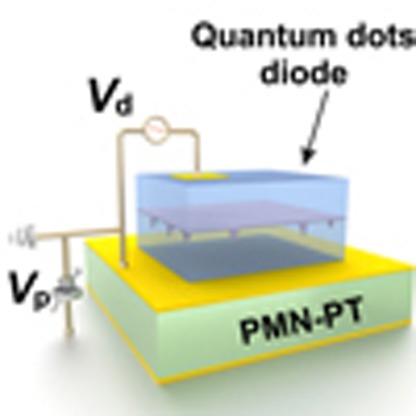 Quantum communications require sources of entangled photons.
Electrically triggered sources usually suffer from low entangled-emission efficiency.
Here, the authors use piezoelectric strains to tune the fine structure of quantum dot
emitters, and increase the entanglement probability and fidelity.
A source of triggered entangled photon pairs is a fundamental element in quantum information science and plays a key role in a number of photonic quantum technologies such as linear quantum computation1, quantum teleportation2 and quantum relays3. So far, generation of polarization-entangled photon pairs is mostly obtained through spontaneous parametric downconversion4 and four-wave mixing5 in nonlinear optical media. At present, these sources are optically driven with lasers, which increases the complexity of the systems. In addition, the nonlinear optical process occurs randomly so that the emission of entangled photon pairs is probabilistic. This results in the generation of zero or multiple entangled-photon pairs in most excitation cycles and unavoidably limits the success of realizing deterministic photonic quantum technologies.
These complications could be alleviated by employing solid-state quantum systems such as colour centres in diamond6, intrinsic defects in silicon carbide7 and semiconductor quantum dots (QDs)8. They exhibit atomic-like optical transitions and therefore allow the generation of deterministic single photons. Most importantly, they can be easily embedded in a light-emitting diode so that electrically driven single-photon emission from these systems can be realized9,10,11. However, to date, colour centres in diamond and intrinsic defects in silicon carbide are limited to emit single photons and the generation of entangled-photon pairs from these two systems has not been demonstrated yet. In contrast, semiconductor QDs are proven candidates for generation of deterministic entangled-photon pairs. In the last decade we have witnessed tremendous advancements in the field, for instance, ultrabright12,13 and highly indistinguishable polarization-entangled photons14 and time-bin entangled photons15 have been demonstrated successfully with semiconductor QDs. Remarkably, a robust and compact entangled-light-emitting-diode (ELED)16 based on semiconductor QDs has been realized, which represents a significant progress in the field of entangled-photon sources. Furthermore, the recent seminal realization of quantum teleportation with ELEDs17,18 has indicated the desirability and the ultimate feasibility of using such ELEDs for various future quantum applications.
In analogy to the cascade emission in atomic systems19, electrical
injection of electrons and holes into an ELED containing QDs switches on the radiative
decay of biexciton (XX) to the exciton (X) and finally to the ground state
(0)20. The two ideally degenerate intermediate X states
(spin±1) ensure emission of polarization-entangled photon pairs and the
two-photon quantum-mechanical state can be expressed with the Bell state  (H and V denote the orthogonally horizontal and vertical
polarizations). In real QDs, however, a reduced structural symmetry due to the
anisotropy in strain, composition and shape results in the appearance of an energetic
splitting between the two bright X states, the so-called fine structure splitting
(FSS)21. In the presence of a FSS, the entangled state evolves over
the X lifetime and the time-averaged fidelity to the Bell state reveals classical
correlations among the emitted photons. High fidelity to the state
|Ψ+〉 can be only observed by temporal post
selection of the emitted photons that, however, results in a strong reduction of the
brightness of the quantum source. Therefore, the FSS in an ELED containing QDs is the
key parameter determining the quality of the entangled-photon pairs. Recent work has
shown that in standard self-assembled QDs22, the probability of finding
QDs with a FSS smaller than the radiative linewidth of the X emission
(1 μeV) is lower than 10−2. This finding
implies that as-grown QDs are still impractical for scalable quantum networks. For
example, it was reported that only one QD per ELED shows an FSS small enough for
entangled-photon generation16. In this context, the real potential of
ELEDs for entangled-photon generation can be harnessed only when a tight control over
the FSS is achieved.
The FSS of semiconductor QDs can be suppressed or tuned to zero via the application of either a vertical electric field23,24 or a combination of strain and electric field25. The main drawback of these approaches is the difficulty of using the electric field to control the FSS and to inject carriers simultaneously, as in ELEDs. Other techniques such as thermal annealing26 and in-plane magnetic field27 would be potentially compatible with the ELEDs, but the former requires a lengthy procedure and the latter bulky setups, thus rendering a practical implementation inconvenient. Recent theoretical works (although not experimentally realized so far) suggest that the FSS can be eliminated using solely a well-controlled strain field28,29. Using piezoelectric-induced strains to engineer the properties of ELEDs would be highly desirable, because this fully electro-mechanically controlled tuning knob would allow the problems related to the FSS in ELEDs to be overcome.
Here we experimentally demonstrate such a quantum device by integrating ELEDs onto a piezoelectric actuator featuring giant piezo-electric response and capable of delivering well-defined anisotropic strain fields. With this device—which we call strain-tunable ELED (ST-ELED)—we show that the FSS of QDs can be tuned effectively with the elastic strain fields without affecting the electrical injection of the operation of the ELEDs. Up to 30% of the QDs are tuned to be suitable for the generation of entangled-photon pairs (more than an order of magnitude more than in previous devices16) and a high operation speed for an entangled-photon source is achieved, that is 400 MHz. This set of properties paves the way towards the exploitation of ELEDs in high data-rate entangled-photon applications involving a large number of quantum emitters.
Results
Self-assembled QDs in strain-tunable diode devices
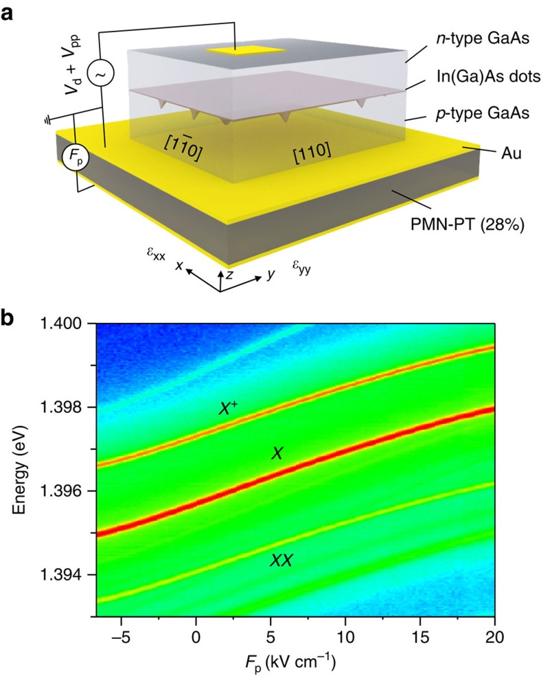
The ST-ELED studied in this work is schematically shown in Fig. 1a. A 440-nm-thick n-i-p nanomembrane containing InGaAs QDs is integrated onto a 0.3-mm-thick [Pb(Mg1/3Nb2/3)O3]0.72[PbTiO3]0.28 (PMN-PT) single piezoelectric crystal. The detailed fabrication process is described in Methods. Different from previous works dealing with strain tuning of QDs via PMN-PTs30,31, the actuator used here has pseudo-cubic cut directions [100], [0-11] and [011], denoted by x, y and z axis, respectively. When the PMN-PT is poled along the z axis, in-plane strain fields with normal components εxx along the x axis and εyy along the y axis with opposite sign can be transferred to the nanomembrane. Accounting for its relevant piezoelectric coefficients d31∼+420 pC N−1 along the x axis and d32∼−1,140 pC N−1 along the y axis32, the in-plane anisotropy is estimated to be εxx≈−0.37εyy. The large and well-controlled strain anisotropy and the broad range of attainable strain magnitudes are unique and turned out to be vital in our work.
Figure 1. Strain-tunable entangled-light-emitting diode.
(a) Sketch of the diode structure. Different from previous works, the PMN-PT top surface has (011) orientation, which imposes large anisotropic strain fields with well-defined orientation onto the overlying ELED. (b) EL from a single QD in an ST-ELED versus electric field Fp applied to the PMN-PT actuator.
Tunable electroluminescence under applied strain fields
Apart from the strain fields, electrical contacts are arranged in such a way that
electrical fields can be independently applied across the diode and the PMN-PT
actuator. By biasing the diode and applying a variable electric field
(Fp) to the PMN-PT simultaneously, energy-tunable
electroluminescence (EL) from a single QD is produced, as shown in Fig. 1b. According to the power and polarization-resolved
measurements the observed EL lines are ascribed to exciton (X), biexciton
(XX) and charged exciton emission
(X+), respectively. As the magnitude of
Fp is varied, all the emission lines shift in energy. In a
first approximation, this shift is due to the strain-induced change of the
energy bandgap of the material, which in turn is proportional to the volumetric
strain
εtot=εxx+εyy+εzz
at the QD position. For in-plane stress and cubic materials,
εtot is given by  which, in the present case, is
  (with
Sij the compliance coefficients of the host
material, see Supplementary Note
1). As εtot has the same sign as
d32, which has a relatively large magnitude and is
negative, we expect a positive Fp to induce a compressive
strain, which results in a blue shift of the EL, whereas a negative
Fp induces a tensile strain, which results in a red shift.
We also note that a total energy shift of about 2.5 meV is achieved
as Fp is varied from −6.7 to
20 kV cm−1.
Changes in polarization and FSS with the strain fields
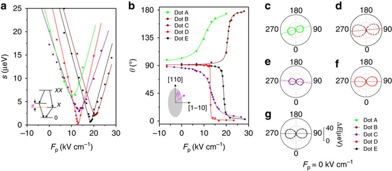
To control the FSS of the QDs embedded in the diode, the crystal axes [1-10] and [110] of the GaAs nanomembrane were carefully aligned along the x and y axes of the PMN-PT actuator, respectively (see Fig. 1a). Representative plots of the FSS (s) of different QDs as a function of Fp are shown in Fig. 2a. Although the emission energy shift is only about 2.5 meV as Fp is varied from −6.7 to 28 kV cm−1 as a consequence of the strong strain anisotropy (and thus relatively small εtot), the FSS is tuned over a broad range from 30 to 0 μeV. Away from the minimum FSS, all studied QDs exhibit an approximately linear change in the FSS with Fp at a rate of about 2.0 μeV kV−1 cm−1, which is about nine times larger than what has been reported for vertical electric fields23. In addition to this drastic change in FSS, we also observe rotations of the exciton polarization angle θ, that is, the polarization direction of the high-energy line of the exciton with respect to the [110] direction of the GaAs nanomembrane (see Fig. 2b). At the largest available tensile (compressive) strain, θ tends to be directed along the [1-10] ([110]) direction for all QDs. Furthermore, we note that the above tuning behaviour is mainly determined by the exciton polarization angle at zero strain fields (θ0) with respect to the predefined direction of the strain29,33. Experimentally, this polarization angle can be extracted from ΔE=|E(φ, Fp=0)−Emin|, where φ is the polarization direction selected by our polarization analyser (which varies from 0° to 360°), E(φ, Fp=0) is the relative position between X and XX as a function of φ and it can be directly extracted from a polarization-resolved EL measurement, and Emin is the minimum energy of E(φ, Fp=0; see Supplementary Fig. 1). Figure 2c–g show ΔE(φ, Fp=0) for the five studied QDs. The initial FSS s0 and θ0 are represented by the magnitude and orientation of the lobes in each polar plot. For the dot A and B, θ0 are 102.0°±0.4° and 92.7°±0.2° (the numbers quoted are the mean±s.d. and the same definition is applied below), respectively, suggesting positive deviations of θ0 from the strain x axis. Consequently, as Fp is increased, the polarization angle θ rotates counterclockwise and the FSS experiences a finite lower bound smin=7.2±0.2 and 2.2±0.1 μeV (the green and wine curves in Fig. 2a,b). For dot C, θ0 is found to be 86.1°±0.4°, which suggests a negative deviation from the strain x axis. Thus, a clockwise rotation of θ over Fp is observed, together with an smin=4.2±0.2 μeV (the purple curve). For the QDs D and E, θ0 is found to be 90.4°±0.3° and 90.6°±0.3° respectively, which indicate exact alignment of θ0 with the strain x axis. The polarization angles for both QDs rotate clockwise as the strain is varied and this implies that their polarization angles at zero strain fields are oriented at angles slightly <90°. It should be noted that this difference from the observed values (larger than 90°) is ascribed to the limited alignment precision of the polarizer (within a few degrees)29. Most importantly, owing to this exact alignment between the exciton polarization angle θ0 and the strain axes for dot D and E, their FSS can be reduced well below 1 μeV and smin is found to be 0.30±0.25 and 0.60±0.20 μeV, respectively. By simply treating the anisotropic strain as an effective uniaxial strain28 (see Supplementary Note 2), the behaviour of s and θ are well fitted (solid lines in Fig. 2a,b). Noticeably, the minimum reachable FSS value, following the form smin=s0|sin(2θ0)|, is determined by s0 and θ0 (see Supplementary Table 1). Even more, the smin predicted before varying the strain fields are 8.18±0.20, 2.34±0.21, 3.3±0.18, 0.24±0.32 and 0.76±0.15 μeV for dot A, B, C, D and E, respectively, which show excellent agreement with our experimental data. From our experimental observations and theoretical analysis, it is clear that, to cancel the FSS with our external strain fields, the strain principal axes should be as close as possible to the polarization angle of QDs at zero applied stress.
Figure 2. Strain-induced change of fine structure splitting and exciton polarization angle.
(a,b) Representative variation of s and the polarization direction θ of the high-energy component of the exciton as a function of Fp for five QDs. The insets show sketches of biexciton cascade and the orientation of the exciton polarization. (c–g) s0 and θ0 for the five studied QDs at Fp=0 kV cm−1. In the polar plot 0° corresponds to the [110] axis and 90° to the [1-10] crystal axis of the GaAs nanomembrane.
Quantum state tomography measurments
The ability to tune the FSS of the QDs to zero allows us to investigate the
capability of the ST-ELED to generate polarization-entangled photon pairs
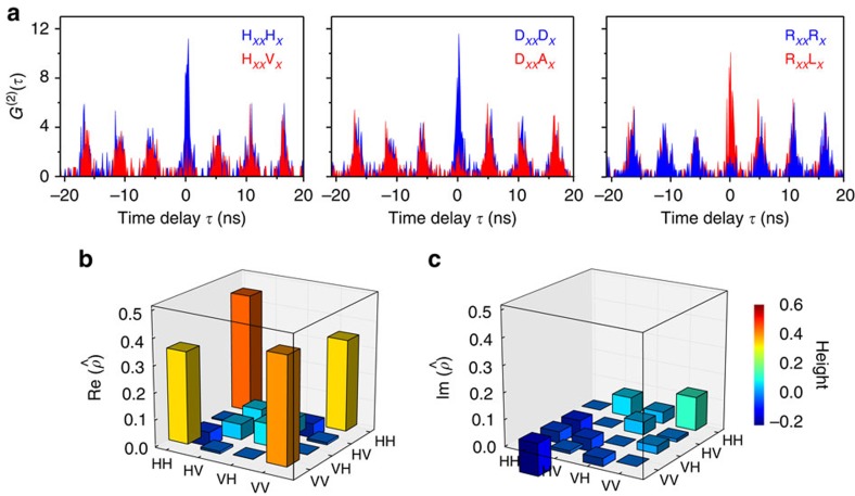
without the aid of post-filtering techniques34,35. Figure 3a shows the polarization resolved co- and
cross-polarization correlation between the XX and X photons
emitted by dot E under electrically pulsed excitation and tuned to a FSS of
0.60±0.20 μeV (at
Fp=18.7 kV cm−1).
The periodic correlation peaks with well-separated temporal distance of
5.4 ns arise from the chosen repetition rate of 185.2 MHz.
Importantly, for co-polarized two-photon, strong correlations are observed in
linear (HV) and diagonal (DA) bases, while strong anti-correlations are observed
in circular basis (RL), as expected for the photon pairs emitted in the
maximally entangled Bell state |Ψ+〉. To
quantify the degree of polarization entanglement, we have reconstructed the
two-photon density matrix by performing quantum state tomography measurements,
as described in ref. 36. Sixteen polarization
correlation measurements were performed and the density matrix is reconstructed
using a maximum likelihood estimation. The imaginary part and the real part of
the density matrix are displayed in Fig. 3b,c. The outer
off-diagonal elements in the real part of the density matrix reveal a high
probability for a superposition of the two-photon wave function, being a clear
signature of polarization entanglement36. Specifically, the
density matrix can be used to quantify the degree of entanglement by extracting
the tangle T, the concurrence C, the largest eigenvalue
λ and the Peres criterion P. We find
C=0.688±0.040 (>0),
T=0.474±0.055 (>0),
λ=0.795 (>0.5) and
P=−0.30±0.02 (<0). All these tests
exceed the classical limit, proving that the quantum state obtained in our
experiment is highly entangled. Using the largest eigenvalue, we are able to
determine the most probable state of the system:  ,
in which the presence of the phase
ϕ0=−0.11π is
likely to be due to the reflection at the beam splitter37 and the
residual FSS 38. As a consequence, the fidelity to the maximally
entangled Bell state |Ψ+〉 is found to
be f+=0.766±0.051.
Figure 3. ST-ELED as source of polarization entangled photons.
(a) Co-polarized (blue) correlation and cross-polarized (red)
correlation counts (G(2)(τ)) for a QD
in an ST-ELED excited with electrical pulses with 185.2 MHz
repetition rate, measured in the rectilinear, diagonal and circular bases.
Representative density matrix  : (b)
real part and (c) imaginary part, which are reconstructed with 16
coincidence counts integrated in a 1.8-ns temporal window centred at 0 delay
time.
High yield of QDs for entangled-photon generation
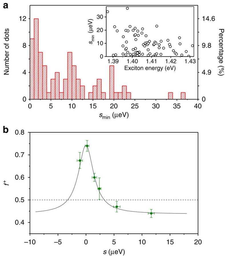
Having demonstrated generation of entangled-photon pairs from our ST-ELED, we present one of the most important results of our work, that is, the capability of anisotropic strain fields to tune about 30% of the QDs for entangled-photon emission. A statistical study from 82 randomly selected QDs revealed that the majority of QDs in our ST-ELED device have θ0 oriented close to the [1-10] crystal axis (see Supplementary Fig. 2). Therefore, the alignment of the strain axes parallel (or perpendicular) to the [1-10] crystal axis of the GaAs ensures frequent observation of QDs with low value of smin. Figure 4a shows the statistical investigation of smin, falling into a range of 0 to 40 μeV. Remarkably, nine QDs have smin <1 μeV, which is of the order of the homogenous linewidth of the X emission. Therefore, 11% of dots have sufficiently small FSS for strong entanglement in our device (see Supplementary Note 3, Supplementary Fig. 3 and Supplementary Table 2 for the entanglement results measured for other dots at smin<1 μeV). In addition, recent works have suggested that for InGaAs QDs entanglement is robust and the violation of the classical limit can be achieved for FSS smaller than 3–4 μeV (refs 37, 39). To quantify this probability in our ST-ELEDs, we use the following approach: we study the evolution of the fidelity to the maximally entangled Bell state |Ψ+〉 as a function of the FSS for one single QD and we use the obtained result to estimate at which value of the FSS it is possible to overcome the classical limit. To determine the entanglement fidelity, polarization correlations were performed for each value of the FSS and entanglement was equivalently quantified by measuring the degree of correlation (see Methods). As shown in Fig. 4b, the maximum fidelity f+=0.75±0.02 is achieved when the FSS is tuned close to zero. For FSS values larger than 3 μeV, the fidelity drastically decreases below the classical limit (see the dashed line). Taking into account that the exciton lifetime of the InGaAs QDs in our ST-ELED device has typical values of about 1 ns, this FSS of about 3 μeV provides an upper limit to observe entanglement, consistent with previous reports for InGaAs QDs12,27,37,39. From the statistical investigation we find that 27 QDs can be tuned below 3 μeV, which indicates a probability as high as 33% of QDs that can be exploited as entangled-light emitters in our ST-ELEDs. Compared with the only work on ELEDs present in the literature16, the yield demonstrated in our work is more than an order of magnitude higher (a factor of ∼30). This probability is higher than what was reported for highly symmetric pyramidal QDs where, however, electrical injection has not been realized yet40. We note that the yield of dots tuned for entangled-photon generation in our ST-ELED can be further improved by optimizing the alignment of the strain principal axes to the statistical mean value of the initial polarization direction. According to our statistical measurement, the mean value of the initial polarization direction is in fact 92.25° instead of 90° (see Supplementary Fig. 2).
Figure 4. Statistical investigation of the minimum FSS and dependence of the entanglement on the value of FSS.
(a) Histogram of the distribution of the minimum FSS (smin) tuned by the externally induced strain fields in the ST-ELED device and the right y axis corresponds to the histogram probability. The inset is a scatter plot of smin as a function of the X emission energy and smin shows no energy dependence. (b) Fidelity (f+) as a function of s dynamically tuned by the anisotropic strain fields and the solid line is Lorentzian fit with a full width at half maximum of 3.3±0.2 μeV. The dashed line indicates the classical value of 0.5 and the error bars are defined as the s.d.
High speed generation of entangled-photon pairs
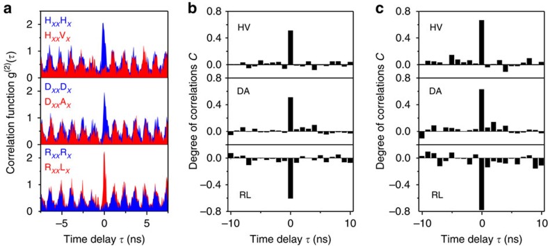
In addition, we can increase the pulsed excitation rate to achieve fast generation rate of the entangled-photon pairs. This feature is highly desirable for high data-rate quantum information processing. Figure 5 shows the results of polarization correlation measurements at 400 MHz for the dot E. Similar to the case of 185.2 MHz, we observe correlations in the HV and DA bases and anti-correlation in the RL basis for co-polarized two photons. In Fig. 5b the degrees of correlation in given bases are reported. We find a state fidelity as high as 0.66±0.02, which exceeds the classical limit of 0.5 and thus proves generation of entangled-photon pairs at 400 MHz. We observe that the fidelity at 400 MHz is smaller than the fidelity at 185.2 MHz reported above. This is likely ascribed to the contribution of a small amount of uncorrelated photon pairs due to the time-dependent re-excitation process, residual FSS and background emission16,38,39. By temporal post selection of the emitted photons we can alleviate these effects for the entanglement degradation. The curves in Fig. 5c show the degrees of correlation for a temporal gate Δτ=0.8 ns at which ∼20% of the coincidence counts are discarded. We measure CHV=0.67±0.06, CDA=0.63±0.04 and CRL=−0.78±0.07, corresponding to f+=0.77±0.03. The degree of correlation and entanglement fidelity can be improved by further shortening Δτ16,13,38,39. With the narrowest available gate width of 0.1 ns applied, ∼80% coincidence counts are discarded and the degrees of correlation increase significantly: CHV=0.74±0.12, CDA=0.74±0.09 and CRL=−0.84±0.12, which provides the highest fidelity of 0.83±0.05. It is interesting to investigate whether such a high level of entanglement is sufficient to violate Bell’s inequality. Using the measured values of the degree of polarization correlation, it is possible to determine Bell parameters SRD, SRC and SDC, which are related to three different planes of the Poincaré sphere (see Methods). Our results show that the Bell parameters increase as the gate width is decreased, and the Bell inequality is found to be violated starting from the gate width of 0.8 ns. From the degrees of correlation at Δτ=0.8 ns, we calculate SRD=1.83±0.07, SRC=2.04±0.09 and SDC=2.00±0.08. Two of these values are >2 and they indicate violations of the Bell inequality. In particular, SRD is found to be less than SRC and SDC, and this is due to the weaker degree of correlation observed in the HV and DA bases (CHV, CDA<|CRL|) (refs 16, 37, 39). This common feature is usually observed for the QDs entangled-photon sources and is most probably ascribed to the weak coupling between the two bright exciton states41. Therefore, for the actual entangled state SRD is not optimally chosen to inspect violation of the Bell inequality. In addition, for the gate width of 0.1 ns, we find SRD=2.09±0.21, SRC=2.23±0.21 and SDC=2.23±0.24 (see Supplementary Fig. 4). All these three parameters are above the threshold of 2, thus proving that our ST-ELED is capable of generating non-local states of light in response to an electrical trigger.
Figure 5. Polarization correlation results from the ST-ELED under electrically pulsed injection at repetition rate of 400 MHz.
(a) Normalized correlation functions for co- and cross-polarized XX and X photons in HV, DA and RL bases. (b,c) Degree of correlation C in given basis, in which correlation in HV and DA bases (C>0) and anti-correlation (C<0) in RL basis are obtained without temporal gate (Δτ=2.5 ns) and with a temporal gate width Δτ=0.8 ns centred at 0 delay time, respectively.
Discussion
We have presented ST-ELEDs in which anisotropic strain fields are used to tune QDs for entangled-photon generation. We have shown that up to 30% of QDs embedded in this device are capable of emitting polarization entangled-photon pairs. This practically removes the tedious search for special QDs plaguing previous ELEDs16. Furthermore, we demonstrate triggered entangled-photon emission at a repetition rate of 400 MHz. Our all electrically controlled ST-ELEDs emerge as one of the most practical entangled-photon sources with fast operation speed and great potential for large-scale quantum communication and computation tasks.
Despite the considerable advances in our ST-ELED, it should be noted that the high yield of QDs tuned for entangled-photon emission has been achieved by applying different magnitudes of strain to different QDs in the single ST-ELED device due to the structural randomness of the QDs. To achieve scalable on-chip integrative entangled-photon applications, active engineering efforts are required to fabricate well-defined microstructures on PMN-PT crystal so that different strain fields can be exerted to different QDs simultaneously on one single chip. This will be of particular interest for realizing QDs arrays of independently tunable electrically triggered entangled-photon sources. Further improvements to the ST-ELED devices, such as integration with microcavities42,43 or micro-lenses44, to achieve bright entangled-photon emission, using III-nitride QDs to develop entangled-photon sources operating at room temperature45,46, constitute important steps towards realizing more practical electrically driven entangled-photon sources for scalable quantum information applications.
Methods
Sample and device fabrication
The studied sample was grown on a (001) GaAs substrate by solid-source molecular beam epitaxy. It consisted of a p-i-n heterostructure diode composed of a 178-nm-thick n-type GaAs layer, a 160-nm-thick intrinsic GaAs layer and a 96-nm-thick p-type GaAs layer from the bottom to the top. A layer of low-density (∼106–107 cm−2), self-assembled InGaAs QDs was embedded in the middle of the intrinsic GaAs layer. The entire diode structure was grown on a 100-nm-thick Al0.75Ga0.25As sacrificial layer. As for the device processing, first of all, standard ultraviolet photolithography and wet chemical etching were used to fabricate mesa structures with size of 120 × 160 μm2. The longer edge of the GaAs membrane was processed along [110] crystal axis of GaAs and—during the transfer onto the piezoelectric actuator—was carefully aligned along the y axis of the PMN-PT actuator. It is worth noting that the bonded gold layer on the bottom formed a p-contact, whereas the n-type contact was formed by depositing a gold pad with size of 50 × 50 μm2 on the top of the nanomembrane.
Electrically pulsed excitation and spectroscopic measurements
The EL is observed when the diode is biased with a DC voltage (Vd) above −1.7 V; however, it is slightly different from one device to another due to the different bonding conditions. The pulsed electrical excitation is accomplished by superimposing an ultrafast electrical pulse stream onto a −1.6 V DC bias by using a broad bandwidth bias-Tee. The pulse stream used in this work has nominal duration of 300 ps and amplitude of Vpp=−8.0 V. The large magnitude of the pulse stream used here is caused by the low pulse injection efficiency, which is probably ascribed to the imperfect electrical connections and large impedance mismatching between the device and the external electronics. Further improvements, including optimization of the electrical connections and introducing an impedance matching network47, are expected to increase the pulse injection efficiency and consequently reduce the pulse magnitude.
In optical measurements, the EL emitted from the diode is collected by a × 50 microscope objective with numerical aperture of 0.42, which is placed on the top of the nanomembrane and collects the photon emission from the area close to the metal contact. By inserting a half-wave plate and a linear polarizer directly after the collection lens, polarization-resolved measurements were performed to obtain the FSS against Fp. The exciton polarization is determined by aligning the fast optical axis of the polarizer along [110] direction of the nanomembrane. The EL was directed to a spectrometer with 750 mm focus length and the spectrum was analysed using a nitrogen-cooled charge-coupled device. The FSS is determined with an accuracy of sub-μeV by taking the experimental procedure in refs 23, 25.
Polarization-resolved photon correlation measurements
Regarding the polarization-resolved correlation measurements, a non-polarizing 50:50 beam splitter is placed directly after the collection objective, to divide the optical paths between two spectrometers, which are used to detect X and XX separately. After each spectrometer, a Hanbury–Brown Twiss setup consisting of a polarizing beam splitter and two high-efficiency single-photon avalanche detectors is placed. Half and quarter waves were used to select the proper polarization basis. The temporal resolution of the system is ∼400 ps. The entanglement can be equivalently quantified by measuring degree of correlation C, which is defined by
 |
where gXX,X(2)(τ)
and 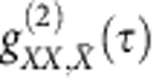 are normalized second-order time correlations
for co-polarized and cross-polarized XX and X photons,
respectively. The fidelity f+ is calculated by
using the formula:
f+=(1+CHV+CDA−CRL),
in which CHV, CDA and CRL
are degree of correlations in HV, DA and RL bases. The Bell parameters are
determined with the formulas:
  ,
,  and
and  .
.
Additional information
How to cite this article: Zhang, J. et al. High yield and ultrafast sources of electrically triggered entangled-photon pairs based on strain-tunable quantum dots. Nat. Commun. 6:10067 doi: 10.1038/ncomms10067 (2015).
Supplementary Material
Supplementary Figures 1-4, Supplementary Tables 1-2, Supplementary Notes 1-3 and Supplementary References.
Acknowledgments
The work was supported financially by BMBF QuaHL-Rep (contract numbers 01BQ1032 and 01BQ1034), Q.Com-H (16KIS0106) and the European Union Seventh Framework Programme 209 (FP7/2007-2013) under grant agreement number 601126 210 (HANAS). J.X.Z. was supported by China Scholarship Council (CSC, number 2010601008). We thank B. Eichler, R. Engelhard, P. Atkinson, B. Höfer and S. Harazim for discussions and the technical support.
The authors declare no competing financial interests.
Author contributions The sample was grown by Y.H. and E.Z., and the device was fabricated by J.X.Z. The work was conceived and designed by J.X.Z., F.D. and R.T., and guided by A.R. and O.G.S. The optical measurements were performed by J.X.Z., J.W., R.T. and D.H. The results were discussed by all authors. J.X.Z. wrote the manuscript with help from all the other authors.
05/11/2016
A correction has been published and is appended to both the HTML and PDF versions of this paper. The error has not been fixed in the paper.
References
- Knill E., Laflamme R. & Milburn G. J. A scheme for efficient quantum computation with linear optics. Nature 409, 46–52 (2001). [DOI] [PubMed] [Google Scholar]
- Bouwmeester D. et al. Experimental quantum teleportation. Nature 390, 575–579 (1997). [Google Scholar]
- Gisin N. & Thew R. Quantum communication. Nat. Photon. 1, 165–171 (2007). [Google Scholar]
- Kwiat P. G. et al. New high-intensity source of polarization-entangled photon pairs. Phys. Rev. Lett. 75, 4337 (1995). [DOI] [PubMed] [Google Scholar]
- Fulconis J., Alibart O., O’Brien J. L., Wadsworth W. J. & Rarity J. G. Nonclassical interference and entanglement generation using a photonic crystal fiber pair photon source. Phys. Rev. Lett. 99, 120501 (2007). [DOI] [PubMed] [Google Scholar]
- Sipahigil A. et al. Indistinguishable photons from separated silicon-vacancy centers in diamond. Phys. Rev. Lett. 113, 113602 (2014). [DOI] [PubMed] [Google Scholar]
- Castelletto S. et al. A silicon carbide room-temperature single-photon source. Nat. Mater. 13, 151–156 (2014). [DOI] [PubMed] [Google Scholar]
- Michler P. et al. A quantum dot single-photon turnstile device. Science 290, 2282–2285 (2000). [DOI] [PubMed] [Google Scholar]
- Mizuochi N. et al. Electrically driven single-photon source at room temperature in diamond. Nat. Photon. 6, 299–303 (2012). [Google Scholar]
- Lohrmann A. et al. Single-photon emitting diode in silicon carbide. Nat. Commun. 6, 7783 (2014). [DOI] [PubMed] [Google Scholar]
- Yuan Z. et al. Electrically driven single-photon source. Science 295, 102–105 (2002). [DOI] [PubMed] [Google Scholar]
- Dousse A. et al. Ultrabright source of entangled photon pairs. Nature 466, 217–220 (2010). [DOI] [PubMed] [Google Scholar]
- Versteegh M. A. M. et al. Observation of strongly entangled photon pairs from a nanowire quantum dot. Nat. Commun. 5, 5289 (2014). [DOI] [PMC free article] [PubMed] [Google Scholar]
- Müller M., Bounouar S., Jöns K. D., Glässl M. & Michler P. On-demand generation of indistinguishable polarization-entangled photon pairs. Nat. Photon. 8, 224–228 (2014). [Google Scholar]
- Jayakumar H. et al. Time-bin entangled photons from a quantum dot. Nat. Commun. 5, 4251 (2014). [DOI] [PMC free article] [PubMed] [Google Scholar]
- Salter C. L. et al. An entangled-light-emitting diode. Nature 465, 594–597 (2010). [DOI] [PubMed] [Google Scholar]
- Stevenson R. M. et al. Quantum teleportation of laser-generated photons with an entangled-light-emitting diode. Nat. Commun. 4, 2859 (2013). [DOI] [PubMed] [Google Scholar]
- Nilsson J. et al. Quantum teleportation using a light-emitting diode. Nat. Photon. 7, 311–315 (2013). [DOI] [PubMed] [Google Scholar]
- Aspect A., Grangier P. & Roger G. Experimental tests of realistic local theories via Bell’s theorem. Phys. Rev. Lett. 47, 460 (1981). [Google Scholar]
- Benson O., Santori C., Pelton M. & Yamamoto Y. Regulated and entangled photons from a single quantum dot. Phys. Rev. Lett. 84, 2513 (2000). [DOI] [PubMed] [Google Scholar]
- Gammon D. et al. Fine structure splitting in the optical spectra of single gaas quantum dots. Phys. Rev. Lett. 76, 3005 (1996). [DOI] [PubMed] [Google Scholar]
- Gong M. et al. Statistical properties of exciton fine structure splitting and polarization angles in quantum dot ensembles. Phys. Rev. B 89, 205312 (2014). [Google Scholar]
- Bennett A. J. et al. Electric-field-induced coherent coupling of the exciton states in a single quantum dot. Nat. Phys. 6, 947–950 (2010). [Google Scholar]
- Ghali M., Ohtani K., Ohno Y. & Ohno H. Generation and control of polarization-entangled photons from GaAs island quantum dots by an electric field. Nat. Commun. 3, 661 (2012). [DOI] [PMC free article] [PubMed] [Google Scholar]
- Trotta R. et al. Universal recovery of the energy-level degeneracy of bright excitons in InGaAs quantum dots without a structure symmetry. Phys. Rev. Lett. 109, 147401 (2012). [DOI] [PubMed] [Google Scholar]
- Young R. J. et al. Inversion of exciton level splitting in quantum dots. Phys. Rev. B 72, 113305 (2005). [Google Scholar]
- Stevenson R. M. et al. A semiconductor source of triggered entangled photon pairs. Nature 439, 179–182 (2005). [DOI] [PubMed] [Google Scholar]
- Gong M., Zhang W., Guo G.-C. & He L. X. Exciton polarization, fine-structure splitting, and the asymmetry of quantum dots under uniaxial stress. Phys. Rev. Lett. 106, 227401 (2011). [DOI] [PubMed] [Google Scholar]
- Trotta R., Martín-Sánchez J., Daruka I., Ortix C. & Rastelli A. Energy-tunable sources of entangled photons: a viable concept for solid-state-based quantum relays. Phys. Rev. Lett. 114, 150502 (2015). [DOI] [PubMed] [Google Scholar]
- Trotta R. et al. Nanomembrane quantum-light-emitting diodes integrated onto piezoelectric actuators. Adv. Mater. 24, 2668–2672 (2012). [DOI] [PubMed] [Google Scholar]
- Zhang J. X. et al. A nanomembrane-based wavelength-tunable high-speed single-photon-emitting diode. Nano Lett. 13, 5808–5813 (2013). [DOI] [PubMed] [Google Scholar]
- Han P., Yan W., Tian J., Huang X. & Pan H. Cut directions for the optimization of piezoelectric coefficients of lead magnesium niobate–lead titanate ferroelectric crystals. Appl. Phys. Lett. 86, 052902 (2005). [Google Scholar]
- Plumhof J. D. et al. Strain-induced anticrossing of bright exciton levels in single self-assembled GaAs/AlxGa1−xAs and InxGa1−xAs/GaAs quantum dots. Phys. Rev. B 83, 121302(R) (2011). [Google Scholar]
- Akopian N. et al. Entangled photon pairs from semiconductor quantum dots. Phys. Rev. Lett. 96, 130501 (2006). [DOI] [PubMed] [Google Scholar]
- Avron J. E. et al. Entanglement on demand through time reordering. Phys. Rev. Lett. 100, 120501 (2008). [DOI] [PubMed] [Google Scholar]
- James D. F. V., Kwiat P. G., Munro W. J. & Andrew W. G. Measurement of qubits. Phys. Rev. A 64, 052312 (2001). [Google Scholar]
- Trotta R. et al. Highly entangled photons from hybrid piezoelectric-semiconductor quantum dot devices. Nano Lett. 14, 3439–3444 (2014). [DOI] [PubMed] [Google Scholar]
- Michler P. Single Semiconductor Quantum Dots Springer (2009). [Google Scholar]
- Hudson A. J. et al. Coherence of an entangled exciton-photon state. Phys. Rev. Lett. 99, 266802 (2007). [DOI] [PubMed] [Google Scholar]
- Juska G. et al. Towards quantum-dot arrays of entangled photon emitters. Nat. Photon. 7, 527–531 (2013). [Google Scholar]
- Young R. J. et al. Bell-inequality violation with a triggered photon-pair source. Phys. Rev. Lett. 102, 030406 (2009). [DOI] [PubMed] [Google Scholar]
- Nowak A. K. et al. Deterministic and electrically tunable bright single-photon source. Nat. Commun. 5, 3240 (2014). [DOI] [PMC free article] [PubMed] [Google Scholar]
- Strauf S. et al. High-frequency single-photon source with polarization control. Nat. Photon. 1, 704–708 (2007). [Google Scholar]
- Gschrey M. et al. Highly indistinguishable photons from deterministic quantum-dot microlenses utilizing three-dimensional in situ electron-beam lithography. Nat. Commun. 6, 7662 (2015). [DOI] [PMC free article] [PubMed] [Google Scholar]
- Kako S. et al. A gallium nitride single-photon source operating at 200 K. Nat. Mater. 5, 887–892 (2006). [DOI] [PubMed] [Google Scholar]
- Deshpande S., Frost T., Hazari A. & Bhattacharya P. Electrically pumped single-photon emission at room temperature from a single InGaN/GaN quantum dot. Appl. Phys. Lett. 105, 141109 (2014). [Google Scholar]
- Ellis D. J. P. et al. Electrically addressing a single self-assembled quantum dot. Appl. Phys. Lett. 88, 133509 (2006). [Google Scholar]
Associated Data
This section collects any data citations, data availability statements, or supplementary materials included in this article.
Supplementary Materials
Supplementary Figures 1-4, Supplementary Tables 1-2, Supplementary Notes 1-3 and Supplementary References.


