Abstract
We design a dual-band absorber formed by combining two cross-shaped metallic resonators of different sizes within a super-unit-cell arranged in mirror symmetry. Simulations indicate that absorption efficiencies greater than 99% can be achieved at two different frequencies under normal incidence. We employ a design scheme with graphene integration, which allows independent tuning of individual absorption frequencies by electrostatically changing the Fermi energy of the graphene layer. High absorbance is maintained over a wide incident angle range up to 50 degrees for both TE and TM polarizations. It thus enables a promising way to design electrically tunable absorbers, which may contribute toward the realization of frequency selective detectors for sensing applications.
Metamaterial absorbers1 have attracted considerable attention in the past few years because of their promising applications in stealth, wavelength selective emission, sensing, and spectroscopy2. A variety of metamaterial-based perfect absorbers have been demonstrated at microwave3,4, terahertz5,6,7,8, infrared9,10,11,12, and visible frequencies13, operating from a single narrow-band to multiband and broadband employing complex super-unit-cells composed of multiple resonators of different sizes14,15,16,17,18,19,20,21,22. There are many techniques to actively and dynamically control the resonance frequency, including optical illumination23,24, mechanically adjustment25,26, fluid filling27, electronic charge injection28, and temperature variations29,30. Among them, electrically tuning is highly desired because of the convenience and high switching rate. Recently, there have been some efforts in investigating tunable metamaterial absorbers based on graphene31,32,33. Graphene, consisting of one monolayer of carbon atoms arranged in a honeycomb lattice, offers unique properties such as high optical transparency, flexibility, high electron mobility34,35, and tunable conductivity36,37. In particular, the electrostatic control of conductivity makes graphene a promising candidate for designing tunable metamaterials at terahertz and infrared frequencies36,38,39,40,41,42,43. Most graphene-based metamaterial absorbers demonstrated single or multiband operation where absorption bands were tuned simultaneously in the same manner. For some applications, such as frequency selective sensing, it may be highly desirable to tune specific absorption bands while keeping others fixed. However, to date there is no extant report on multiband metamaterial absorbers based on graphene that can independently tune absorption bands.
In this paper, we numerically demonstrate, via highly confident numerical simulations, a dual-band metamaterial absorber where the two absorption bands can be independently tuned. This can be accomplished through the application of a voltage bias to modify the conductivity of the graphene layer that has been integrated into the metamaterial absorber super-unit-cell. The metamaterial device offers high absorbance over a wide range of incidence angles, and the independently tunable absorption bands might find applications in fields like tunable sensors and selective thermal emitters.
Results and Discussions
The schematic design of the proposed tunable metamaterial absorber is illustrated in Fig. 1(a), and it consists of a traditional metamaterial absorber architecture with metallic resonators separated from a ground plane by a dielectric spacer. The unit cell of the dual-band absorber contains a combination of two cross-shaped metallic resonators of different sizes (S1 and S2), as shown in Fig. 1(b). They can be configured independently to enable two absorption bands at different frequencies. A monolayer of graphene is placed between the cross-shaped gold resonators and the PTFE dielectric spacer. The thickness of the PTFE dielectric spacer is ts = 0.285 μm, and the thickness of gold is tm = 0.1 μm. The periods along the x and y directions are Px = 14.4 μm and Py = 3.6 μm, the lengths of the bigger and smaller gold crosses are S1 = 3.0 μm and S2 = 2.0 μm, and their widths are W1 = 0.72 μm and W2 = 0.6 μm, respectively. The permittivity of the PTFE spacer is 2. The graphene layer is structured into interdigitated fingers with width Wg = 3.4 μm and spacing d = 0.2 μm. Two gate voltages, Vg1 and Vg2, are applied to the two graphene interdigitated finger sets in order to tune their Fermi energies independently.
Figure 1.
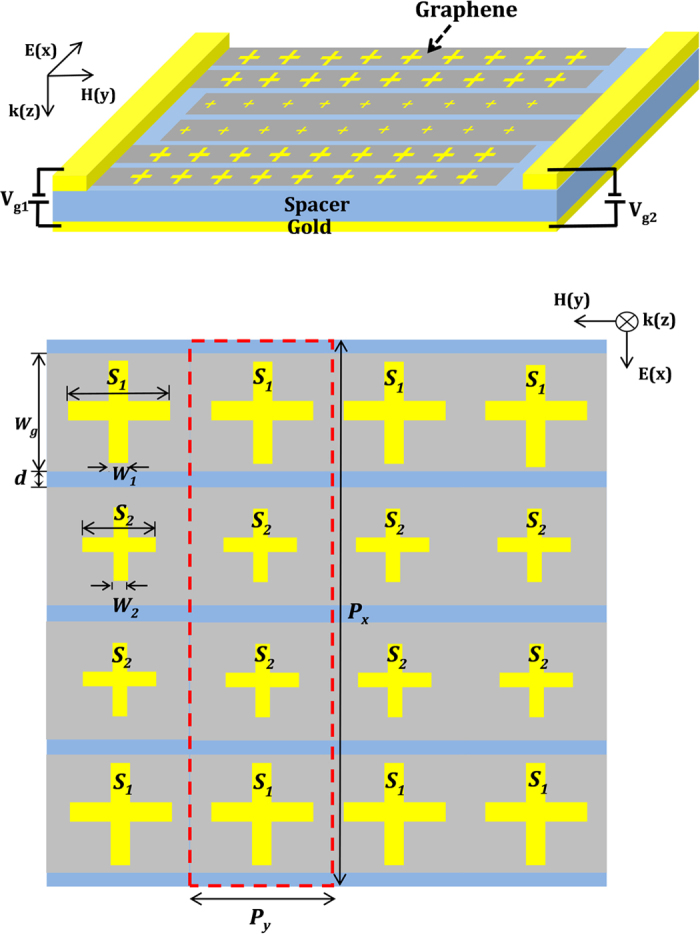
(a) Schematic of the independently tunable dual-band metamaterial perfect absorber consisting of an array of cross-shaped resonator pairs, a dielectric spacer, a gold ground plane, and interdigitated graphene fingers enabling independent voltage bias. (b) Top view of the metamaterial unit cells with dimensions specified. The red dashed box represents a unit cell, containing four crosses (two of each size).
The simulations were carried out using the well-established three-dimensional full wave electromagnetic solver, CST Microwave Studio 2012. We obtained the S parameters (S21 for transmission and S11 for reflection) and the absorbance was derived using  , as the transmission is zero due to the thick gold ground plane.
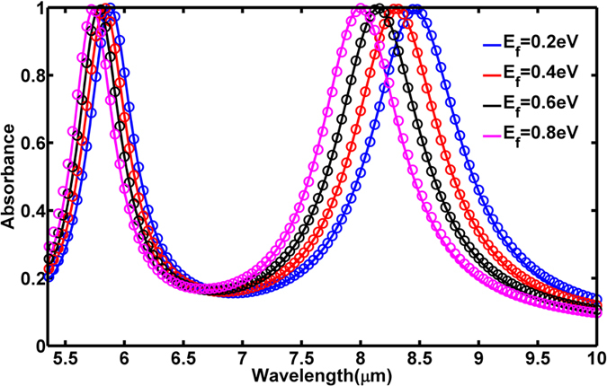
We first investigated a dual-band metamaterial absorber shown in Fig. 1 except that the graphene layer is uniform over the entire sample. The simulated absorbance spectra are plotted as the solid curves in Fig. 2 for various values of Fermi energy. Within the limit of our considered wavelength, the conductivity of the graphene layer is dominated by the intraband conductivity which can be modeled using Drude formula. The conductivity of the graphene was estimated using the calculated plasma frequency (ωp) and the scattering rate (Γ) for various Fermi energy as explained in Methods. By optimizing the thickness of the spacer ts = 0.285 μm, we obtained two absorption bands with peaks absorbance greater than 99%. When Ef = 0.2 eV, the two absorption peaks are positioned at wavelengths of 5.88 μm and 8.46 μm. Varying Ef from 0.2 eV to 0.8 eV, which could be accomplished by applying a voltage bias between the ground plane and graphene layer, both absorption peaks show blue-shift while the high absorbance is remained. The longer wavelength absorption peak shifts by ΔλS1 = 0.46 μm (5.4% shift), and the shorter wavelength absorption peak shifts by ΔλS2 = 0.15 μm (2.6% shift). The difference in the absorption wavelength shift is mostly due to the wavelength dependent change of the imaginary conductivity  , which is larger at longer wavelengths44, a direct consequence of the Drude-like graphene conductivity.
Figure 2. Simulated dual-band absorbance spectra (solid curves) and absorbance in circuit model (circles) at various graphene Fermi energy Ef.
In order to further understand the blue-shift, we describe the metamaterial absorber as a combination of two independent transfer functions, H1 and H2, which apply to the corresponding two resonant structures. The wave reflected from the metamaterial absorber is quantified by
 |
where E0 is the normally incident electric field. The absorbance is then given by  . Each transfer function is calculated by a circuit model, where the cross-shaped resonator is modeled as an RLC circuit shunting a TEM transmission line, as shown in Fig. 3. The graphene layer is modeled by a separate shunt impedance ZG across the capacitor C. The entire circuit is backed by a transmission line of impedance
  and a single load resistor, ZL, representing the gold ground plane. The length of transmission line ZD is equal to the dielectric spacer thickness employed in the simulations and has the same effect of creating a resonant cavity between ZL and the RLC circuit45. This, in combination with the complex impedance of the RLC circuit, enables nearly perfect absorption.
Figure 3. Circuit model employed in the calculation of Hi where i = (1, 2) represent resonators CR1 and CR2, respectively.
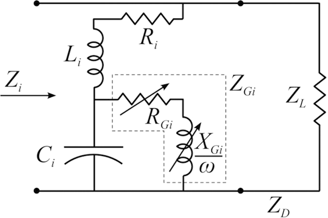
The circuit presents a complex, frequency-dependent impedance Zi to the wave incident from a transmission line of impedance Z0 = 377 Ω. The transfer functions are equivalent to field reflection coefficients
 |
The load impedance ZL = 2 Ω was calculated using tabulated bulk gold conductivity values46 and assuming a wave penetration depth of about 3 skin depths (3δd~100 nm). The graphene impedance consists of real and imaginary parts,
 |
The term Lk = 1/α is the kinetic inductance of the graphene and, being variable with Ef, is the tuning mechanism of the absorber. By the equation for ZG it should be hypothesized that because  ≫
≫  where
where  is the relaxation time, at short wavelengths the resistive part of ZG should play a minor role. However, this should not hold true at longer wavelengths and RG should begin to have a noticeable effect.
The values for Ri, Li, and Ci were determined empirically by matching the resonance frequency, Q-factor, and peak absorbance qualities of both resonances against simulations not involving any graphene layer. It was found that these factors were highly constrained if all three qualities were to be simultaneously matched. Numerical values for ZGi were calculated as
 |
where Bi is a constant fitting parameter that is easily obtained by matching the magnitude of the frequency shift of the absorption peak over Ef = [0.2 : 0.8] eV. After ZGi was determined, the factors Ri, Li, and Ci were fine-tuned to give the final model parameters. These are summarized in Table 1.
Table 1. Empirically determined circuit parameters to match simulations.
| Structure | R (Ω) | L (pH) | C (aF) | B |
|---|---|---|---|---|
| CR1 (big) | 12.5 | 0.935 | 16.2 | 0.751 |
| CR2 (small) | 31.0 | 2.36 | 3.65 | 3.66 |
The equivalent circuit model results are summarized as the circles in Fig. 2. As shown, the model behaves almost exactly as the simulation in every important aspect, including the magnitude of the absorption shift, the maintenance of the absorption peak, and the maintenance of the absorption bandwidth. Importantly, all of these qualities are matched during tuning by changes in the graphene conductivity alone. Several important implications can be drawn from the model, and are not obvious from the simulations. The first is that the two structures behave entirely independent of one another, despite their interdigitated and close patterning. This fact is revealed in the independent treatment of each periodic structure as a separate transfer function. The second is that the graphene predominately alters the capacitive reactance of the structures during tuning. Alternative models, where ZG shunted the entire RLC circuit or the LC sub-circuit, were also studied. In these cases, the absorbance bandwidth and/or the peak absorbance could not be kept constant in tuning over the entire Fermi energy range. By restricting the graphene effect to the capacitor alone, the net inductive reactance of Zi is largely maintained during tuning, being dominated by Li. Though the effective capacitive reactance changes, it has very little effect on the Q-factor. Thus, absorption bandwidth is almost completely unaffected during tuning. The net resistive impedance of Zi is also maintained, being dominated almost entirely by Ri for all values of Ef. This prevents any change in the peak absorbance during tuning. The third implication is the validation of the hypothesis that RG plays a required role in the tuning behavior at long wavelengths. By artificially zeroing RG in the circuit model, a negligible effect was observed on the CR2 resonant absorbance, whereas the CR1 resonant absorbance peak continually decayed during tuning.
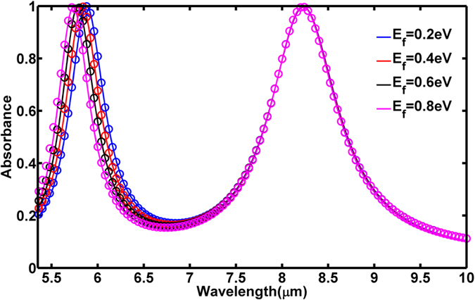
To investigate the independent tuning of each resonance, we adopt the device design shown in Fig. 1(a), where the graphene layer is structured in interdigitated fingers. Every pair of fingers of graphene contains metallic resonators of the same size. These alternate finger pairs are connected at the far ends using metallic bus-lines; therefore, all bigger resonators (CR1) are electrically separated from smaller resonators (CR2). The design allows tuning the Fermi energy of graphene layers under bigger and smaller resonators independently using bias Vg1 and Vg2, respectively. First, we calculated the absorbance spectrum of our absorber by changing the Fermi energy of graphene under the small resonators (CR2) via tuning bias voltage Vg2, while keeping the Fermi energy of graphene under the bigger resonators (CR1) fixed to be 0.5 eV. The simulated absorbance spectra are shown as the solid curves in Fig. 4, having two strong absorption peaks for each particular Fermi energy. As the Fermi energy of graphene under the small resonators increases from 0.2 eV to 0.8 eV, the resonant frequency related to CR2 resonator blue-shifts from λ2 = 5.88 μm to λ2 = 5.73 μm, a wavelength shift of 2.6%. An alternative expression of modulation is obtained by fixing the observation wavelength to λ2 = 5.88 μm. In this case one would observe an absorbance change  of 29% during tuning. The Fermi energy of the graphene layer under the CR1 resonators is fixed, so the resonance at λ1 = 8.23 μm arising from the bigger resonators remains nearly invariant. This implies that the two resonances are spectrally separated enough to prevent any noticeable mutual coupling. Thus we can independently tune the resonant frequency of the CR2 resonator by changing the Fermi energy of graphene under the small crosses. The same results can be obtained from the circuit model by fixing the Fermi energy of H1 to be 0.5 eV, which are shown as the circles in Fig. 4.
Figure 4. Simulated dual-band absorbance spectra (solid curves) and absorbance spectra in circuit model (circles) tuned by Fermi energy of graphene under the smaller cross-shape resonators (CR2).
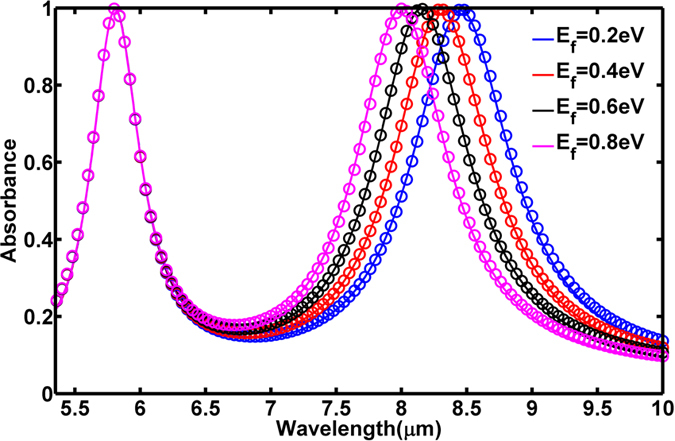
Next, we calculated the absorption while varying the Fermi energy of the graphene layer under the bigger resonators (CR1) while fixing the Fermi energy of graphene under the smaller resonators (CR2) to 0.5 eV. The simulated absorbance spectra for various Fermi energies are shown as the solid curves in Fig. 5. As the Fermi energy of graphene under the CR1 resonator increases from 0.2 eV to 0.8 eV, its resonant wavelength λ1 blue-shifts from 8.45 μm to 8.0 μm, a wavelength shift of 5.3%. An alternative expression of modulation is obtained by fixing the observation wavelength to λ1 = 8.45 μm. In this case one would observe an absorbance change  of 50% during tuning for the bigger resonator while keeping the resonant wavelength of smaller resonator fixed. The same results can be obtained from the circuit model by using the same parameters, which are shown as the circles in Fig. 5. The number of independently tunable resonators can be further increased by a multilayered approach to extend spectral coverage; however, this will require more complex design and increase fabrication difficulties.
Figure 5. Simulated dual-band absorbance spectra (solid curves) and absorbance spectra in circuit model (circles) tuned by Fermi energy of graphene under the big cross-shape resonators (CR1).
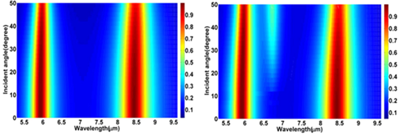
We have conducted additional simulations to investigate the behavioral dependence on angle of incidence. For these simulations we fix the Fermi energy of graphene under both resonators to be 0.4 eV, while maintaining all other aforementioned parameters. Absorbance as a function of wavelength and incident angle is shown in Fig. 6(a,b) under TE and TM polarizations, respectively. The two red regions in each of the figures show that absorbance in both bands remains strong from 0 to 50 degrees. Nearly 90% absorbance is still obtained at large incidence angles for both of the two resonance peaks under TE and TM polarizations We have investigated the incident angle-dependent absorbance for various Fermi energies (result not shown here) and have not observed any Fermi energy related discontinuity in the absorption bands that were noticed in earlier demonstration33. Therefore, our design offers a better robustness for oblique incidence for both TE and TM polarizations.
Figure 6. Absorbance spectrum as a function of wavelength and incident angle under (a) TE and (b) TM polarization for Ef = 0.4 eV.
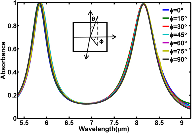
It should be noted that polarization-insensitive absorbers are highly desirable47,48,49,50,51. To show this property, we scanned the azimuthal angle φ from 0° to 90°. The corresponding absorbance spectra are shown in Fig. 7. Here, azimuthal angle φ = 0° represents the incident electric field along x-axis and φ = 90° represents the incident electric field along y-axis. The simulated result shows that the dual-band absorbance remains nearly unchanged with the variation of azimuthal angle. Thus we can conclude that the metamaterial absorber is highly polarization independent.
Figure 7. Absorbance spectra versus wavelength at different azimuthal angles φ.
We also note that the scattering rate of graphene may vary due to the impurities, defects, and interfaces52. To show the validity of our design, we performed numerical simulations for a similar structure by setting the graphene scattering rate  THz (a 6.2 × increase). The results (not shown here) reveal similar frequency and amplitude tuning, indicating that our design is applicable for tunable devices with realistic graphene films.
Conclusions
In conclusion, we showed that a dual-band absorber can be formed by using horizontally cascaded cross-shaped resonant structures at mid-infrared frequencies. Absorption peaks of greater than 99% were obtained under normal incidence, and high absorbance remained at large incident angles up to 50 degrees for both of the bands under TE and TM polarizations. Moreover, our metamaterial absorber structure enabled independent tunability of the two absorption bands by electrically controlling the Fermi energy of corresponding graphene layers. With its excellent performance, our design should be applicable in many fields such as tunable sensors and selective thermal emitters.
Methods
The simulations were carried out using commercial Finite Element full wave electromagnetic solver CST Microwave Studio 2012. We employed a time-domain solver to obtain frequency-dependent absorption spectra in Figs 2, 4 and 5 under normal incidence. The incident angle dependent absorptions in Fig. 6 were calculated using a frequency-domain solver by necessity to accommodate the oblique incidence angle. To check consistency, we compared the simulated absorptions obtained from both time- and frequency-domain at normal incidence for various Fermi energies. The results agreed very well. For the time-domain solver, we applied perfect electrical and perfect magnetic boundary conditions along the x and the y directions, respectively, with an open boundary condition in the z direction. For the frequency-domain solver, we adopted unit-cell boundary conditions in the x and y directions with Floquet ports in the z directions. The thickness of graphene layer was set to tg = 0.5nm for all of our simulations. The effective dielectric constant of graphene can be calculated by  , where tg is the thickness of graphene.
The complex surface conductivity of graphene can be calculated from the well-known Kubo formula and is described with interband and intraband contributions as32
 |
 |
 |
where
 |
ω is the angular frequency, Ef is the Fermi energy of graphene, Γ is the collision angular frequency, T is the temperature, kB is the Boltzmann constant, e is the elementary charge, and  is the reduced Planck’s constant. When the Fermi energy is greater than half of the photon energy,
  < 2Ef, the intraband contribution dominates the graphene conductivity as the interband transitions are negligible due to Pauli blocking53. This condition could be approximately satisfied if we set Ef >0.2 eV for wavelengths of interest ranging from 5.5 μm to 10 μm. Then, graphene can be described by taking only the intraband part of the Drude-like conductivity as described in Eq. (6). We can obtain the graphene plasma frequency from
 |
where tg = 0.5 nm is the thickness of graphene layer. In our simulations, we set T = 300 K and scattering  (i.e.,
  THz)44.
The relationship of the Fermi energy  of the graphene and the voltage bias
  satisfy the following equation33
 |
where  is the Planck’s constant,
  is the Fermi velocity (~1.1 × 10⁶ m/s),
  and
and  are the permittivity of the spacer and vacuum respectively. Generally, the chemical potential can be tuned over a wide range (typically from −1 eV to 1 eV)53,54,55. Therefore one can set the Fermi energy near 0.5 eV chemically and then tune Fermi energy from 0.2 eV to 0.6 eV by applying corresponding voltage bias of −240 V to +240 V. To avoid dielectric breakdown of the spacer we also plan to use SiO2 and Kapton which require lower voltage bias while offering higher dielectric breakdown for our experimental demonstration. A recent demonstration shows that the gate voltage bias can be significantly reduced by applying a layer of ionic gel over graphene film with top gating architecture56, which can be easily adapted to our design.
Additional Information
How to cite this article: Zhang, Y. et al. Independently tunable dual-band perfect absorber based on graphene at mid-infrared frequencies. Sci. Rep. 5, 18463; doi: 10.1038/srep18463 (2015).
Acknowledgments
We acknowledge partial support from the Los Alamos National Laboratory LDRD program. This work was performed, in part, at the Center for Integrated Nanotechnologies, a U.S. Department of Energy, Office of Basic Energy Sciences user facility. Los Alamos National Laboratory, an affirmative action equal opportunity employer, is operated by Los Alamos National Security, LLC, for the National Nuclear Security Administration of the U.S. Department of Energy under Contract No. DE-AC52-06NA25396. We also acknowledge partial support from the Natural Science Foundation of Shandong Province, China (Grant No. ZR2012FM011), Qingdao city innovative leading talent plan(13-CX-25), the CAEP THz Science and Technology Foundation (Grant No. 201401), Qingdao Economic & Technical Development Zone Science & Technology Project (Grant No. 2013-1-64), the Shandong University of Science and Technology Foundation, China (Grant No. YC140108), and the China Scholarship Council. We also gratefully acknowledge fruitful discussion with Akhilesh Singh.
Footnotes
Author Contributions Y.Z. and A.K.A. generated the idea wrote the manuscript text. T.L and E.A. designed the devices and performed numerical simulations. J.F.O and E.A. developed the circuit model. H.Z., Q.C., A.J.T. and H.T.C. discussed the design of proposed structure and simulation results, as well as contributed in manuscript preparation. All authors discussed the results and substantially contributed to the manuscript.
References
- Landy N. I., Sajuyigbe S., Mock J. J., Smith D. R. & Padilla W. J. Perfect metamaterial absorber. Phys. Rev. Lett. 100, 207402 (2008). [DOI] [PubMed] [Google Scholar]
- Watts C. M., Liu X. & Padilla W. J. Metamaterial electromagnetic wave absorbers. Adv. Mater. 24, OP98–OP120 (2012). [DOI] [PubMed] [Google Scholar]
- Alici K. B., Bilotti F., Vegni L. & Ozbay E. Experimental verification of metamaterial based subwavelength microwave absorbers. J. Appl. Phys. 108, 083113 (2010). [Google Scholar]
- Xu Y. Q., Zhou P. H., Zhang H. B., Chen L. & Deng L. J. A wide-angle planar metamaterial absorber based on split ring resonator coupling. J. Appl. Phys. 110, 044102 (2011). [Google Scholar]
- Landy N. I. et al. J. Design, theory, and measurement of a polarization-insensitive absorber for terahertz imaging. Phys. Rev. B 79, 125104 (2009). [Google Scholar]
- Diem M., Koschny T. & Soukoulis C. M. Wide-angle perfect absorber/thermal emitter in the terahertz regime. Phys. Rev. B 79, 033101 (2009). [Google Scholar]
- Shchegolkov D. Y., Azad A. K., O’Hara J. F. & Simakov E. I. Perfect subwavelength fishnetlike metamaterial-based film terahertz absorbers. Phys. Rev. B 82, 205117 (2010). [Google Scholar]
- Tao H. et al. A metamaterial absorber for the terahertz regime: Design, fabrication and characterization. Opt. Express 16, 7181–7188 (2008). [DOI] [PubMed] [Google Scholar]
- Zhu W. & Zhao X. Metamaterial absorber with dendritic cells at infrared frequencies. J. Opt. Soc. Am. B 26, 2382–2385 (2009). [Google Scholar]
- Liu N., Mesch M., Weiss T., Hentschel M. & Giessen H. Infrared perfect absorber and its application as plasmonic sensor. Nano Lett. 10, 2342–2348 (2010). [DOI] [PubMed] [Google Scholar]
- Hao J. et al. High performance optical absorber based on a plasmonic metamaterial. Appl. Phys. Lett. 96, 251104 (2010). [Google Scholar]
- Liu X., Starr T., Starr A. F. & Padilla W. J. Infrared spatial and frequency selective metamaterial with near-unity absorbance. Phys. Rev. Lett. 104, 207403 (2010). [DOI] [PubMed] [Google Scholar]
- Gong Y. et al. Highly flexible all-optical metamaterial absorption switching assisted by Kerr-nonlinear effect. Opt. Express 19, 10193–10198 (2011). [DOI] [PubMed] [Google Scholar]
- Huang L. et al. Impact of resonator geometry and its coupling with ground plane on ultrathin metamaterial perfect absorbers. Appl. Phys. Lett. 101, 101102 (2012). [Google Scholar]
- Wang B. X. et al. A simple design of a broadband, polarization-insensitive, and low-conductivity alloy metamaterial absorber. Appl. Phys. Express 7, 082601 (2014). [Google Scholar]
- Zhang B. et al. Polarization-independent dual-band infrared perfect absorber based on a metal-dielectric-metal elliptical nanodisk array. Opt. Express 19, 15221–15228 (2011). [DOI] [PubMed] [Google Scholar]
- Wang B. X. et al. Theoretical investigation of broadband and wide-angle terahertz metamaterial absorber. IEEE Photonic. Tech. L. 26, 111–114 (2014). [Google Scholar]
- Zhu J. et al. Ultra-broadband terahertz metamaterial absorber. Appl. Phys. Lett. 105, 021102 (2014). [Google Scholar]
- Dayal G. & Ramakrishna S. A. Design of multi-band metamaterial perfect absorbers with stacked metal–dielectric disks. J. Opt. 15, 055106 (2013). [Google Scholar]
- Wen Q. Y., Zhang H. W., Xie Y. S., Yang Q. H. & Liu Y. L. Dual band terahertz metamaterial absorber: Design, fabrication, and characterization. Appl. Phys. Lett. 95, 241111 (2009). [Google Scholar]
- Shen X. et al. Triple-band terahertz metamaterial absorber: Design, experiment, and physical interpretation. Appl. Phys. Lett. 101, 154102 (2012). [Google Scholar]
- Liu X. et al. Taming the blackbody with infrared metamaterials as selective thermal emitters. Phys. Rev. Lett. 107, 045901 (2011). [DOI] [PubMed] [Google Scholar]
- Chen H. T. et al. Experimental demonstration of frequency-agile terahertz metamaterials. Nat. Photonics, 2, 295–298 (2008). [Google Scholar]
- Zhao Y. et al. Light-driven tunable dual-band plasmonic absorber using liquid-crystal-coated asymmetric nanodisk array. Appl. Phys. Lett. 100, 053119 (2012). [Google Scholar]
- Li J. et al. Mechanically tunable terahertz metamaterials. Appl. Phys. Lett. 102, 121101 (2013). [Google Scholar]
- Zhang F. et al. Mechanically stretchable and tunable metamaterial absorber. Appl. Phys. Lett. 106, 091907 (2015). [Google Scholar]
- Chronis N., Liu G., Jeong K. H. & Lee L. Tunable liquid-filled microlens array integrated with microfluidic network. Opt. Express 11, 2370–2378 (2003). [DOI] [PubMed] [Google Scholar]
- Chen H. T. et al. Active terahertz metamaterial devices. Nature 444, 597–600 (2006). [DOI] [PubMed] [Google Scholar]
- Driscoll T. et al. Dynamic tuning of an infrared hybrid-metamaterial resonance using vanadium dioxide. Appl. Phys. Lett. 93, 024101 (2008). [Google Scholar]
- Kocer H. et al. Thermal tuning of infrared resonant absorbers based on hybrid gold-VO2 nanostructures. Appl. Phys. Lett. 106, 161104 (2015). [Google Scholar]
- Alaee R., Farhat M., Rockstuhl C. & Lederer F. A perfect absorber made of a graphene micro-ribbon metamaterial. Opt. Express 20, 28017–28024 (2012). [DOI] [PubMed] [Google Scholar]
- Andryieuski A. & Lavrinenko A. V. Graphene metamaterials based tunable terahertz absorber: effective surface conductivity approach. Opt. Express 21, 9144–9155 (2013). [DOI] [PubMed] [Google Scholar]
- Zhang Y., Feng Y., Zhu B., Zhao J. & Jiang T. Graphene based tunable metamaterial absorber and polarization modulation in terahertz frequency. Opt. Express 22, 22743–22752 (2014). [DOI] [PubMed] [Google Scholar]
- Novoselov K. S. et al. A roadmap for graphene. Nature 490, 192–200 (2012). [DOI] [PubMed] [Google Scholar]
- Geim A. K. Graphene: status and prospects. Science 324, 1530–1534 (2009). [DOI] [PubMed] [Google Scholar]
- Lee S. H. et al. Switching terahertz waves with gate-controlled active graphene metamaterials. Nat. Mater. 11, 936–941 (2012). [DOI] [PubMed] [Google Scholar]
- Sensale-Rodriguez B. et al. Unique prospects for graphene-based terahertz modulators. Appl. Phys. Lett. 99, 113104 (2011). [Google Scholar]
- Valmorra F. et al. Low-bias active control of terahertz waves by coupling large-area CVD graphene to a terahertz metamaterial. Nano Lett. 13, 3193–3198 (2013). [DOI] [PubMed] [Google Scholar]
- Cakmakyapan S., Caglayan H. & Ozbay E. Coupling enhancement of split ring resonators on graphene. Carbon 80, 351–355 (2014). [Google Scholar]
- Yao Y. et al. Electrically Tunable Metasurface Perfect Absorbers for Ultrathin Mid-Infrared Optical Modulators. Nano Lett. 14, 6526–6532 (2014). [DOI] [PubMed] [Google Scholar]
- Liu M., Yin X. & Zhang X. Double-layer graphene optical modulator. Nano Lett. 12, 1482–1485 (2012). [DOI] [PubMed] [Google Scholar]
- Sensale-Rodriguez B. Graphene-insulator-graphene active plasmonic terahertz devices. Appl. Phys. Lett. 103, 123109. (2013). [Google Scholar]
- Yang K., Liu S., Arezoomandan S., Nahata A. & Sensale-Rodriguez B. Graphene-based tunable metamaterial terahertz filters. Appl. Phys. Lett. 105, 093105 (2014). [Google Scholar]
- Vasić B. & Gajić R. Graphene induced spectral tuning of metamaterial absorbers at mid-infrared frequencies. Appl. Phys. Lett. 103, 261111 (2013). [Google Scholar]
- Chen H. T. Interference theory of metamaterial perfect absorbers. Opt. Express 20, 7165–7172 (2012). [DOI] [PubMed] [Google Scholar]
- Ordal M. A. et al. Optical properties of the metals al, co, cu, au, fe, pb, ni, pd, pt, ag, ti, and w in the infrared and far infrared. Appl. Opt. 22, 1099–1119 (1983). [DOI] [PubMed] [Google Scholar]
- Shen X. et al. Polarization-independent wide-angle triple-band metamaterial absorber. Opt. Express. 19, 9401–9407 (2011). [DOI] [PubMed] [Google Scholar]
- Shen X. et al. Triple-band terahertz metamaterial absorber: Design, experiment, and physical interpretation. Appl. Phys. Lett. 101, 154102 (2012). [Google Scholar]
- Li H. et al. Ultrathin multiband gigahertz metamaterial absorbers. J. Appl. Phys. 110, 014909 (2011). [Google Scholar]
- Cui T. J., Qi M. Q., Wan X., Zhao J. & Cheng Q. Coding metamaterials, digital metamaterials and programmable metamaterials. Light: Science & Applications, 3, e218 (2014). [Google Scholar]
- Liu S., Chen H. & Cui T. J. A broadband terahertz absorber using multi-layer stacked bars. Appl. Phys. Lett. 106, 151601 (2015). [Google Scholar]
- Lin I. T., Lai Y. P., Wu K. H. & Liu J. M. Terahertz Optoelectronic Property of Graphene: Substrate-Induced Effects on Plasmonic Characteristics. Appl. Sci. 4, 28–41 (2014). [Google Scholar]
- Yao Y. et al. Broad electrical tuning of graphene-loaded plasmonic antennas. Nano Lett. 13, 1257–1264 (2013). [DOI] [PubMed] [Google Scholar]
- Cheng H. et al. Dynamically tunable broadband mid-infrared cross polarization converter based on graphene metamaterial. Appl. Phys. Lett. 103, 223102 (2013). [Google Scholar]
- Li Q. et al. Active graphene-silicon hybrid diode for terahertz waves. Nat. Commun. 6, 7082 (2015). [DOI] [PMC free article] [PubMed] [Google Scholar]
- Thareja V. et al. Electrically Tunable Coherent Optical Absorption in Graphene with Ion Gel. Nano Lett. 15, 1570–1576 (2015). [DOI] [PubMed] [Google Scholar]


