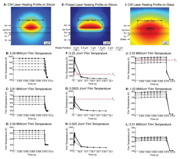
Figure 2.
Simulated heat distribution in np-Au film in response to CW (A) and pulsed (E) laser irradiation on silicon as well as CW irradiation on glass (I). Resulting film temperature profiles are shown for 5.09 MW/cm2 (B), 3.81 MW/cm2 (C), 2.54 MW/cm2 (D) for the CW mode on silicon, 0.25 J/cm2 (F), 0.0625 J/cm2 (G), 0.025 J/cm2 (H) for the pulsed mode on silicon and 2.03 MW/cm2 (J), 1.02 MW/cm2 (K), 0.51 MW/cm2 (L) and glass respectively. A red dashed line denotes the melting temperature (1337 K) of bulk Au.

