Abstract
Ferroelectric polarization switching and its domain evolution play a key role on the macroscopic electric properties of ferroelectric or piezoelectric devices. Mechanical switching has been reported recently in ~5 nm BaTiO3 and PbZr0.2Ti0.8O3 epitaxial films; however it is still a challenge for a mechanical force to switch polarization of a slightly thicker film in the same way as an electric field. Here, we report that the polarization of a 70 nm BiFeO3 epitaxial film can be completely switched by a mechanical force, and its domain evolution is similar to that observed with electrical switching. With the gradual increase of the field/force, new domains nucleate preferentially at domain boundaries, the μm-size domains commonly decompose to a mass of nm-size domains, and finally they may reorganize to μm-size domains which undergo 180o polarization switching through multi steps. Importantly, the complete mechanical switching of polarization was also established in the (0 0 1) film with a smooth surface. Furthermore, either upward or downward polarization can be read out nondestructively by a constant current. Our study sheds light on prospective applications of ferroelectrics in the absence of an electric field, such as memory devices and other micro-electromechanical systems.
Ferroelectrics are widely used in electronic, sensing and machinery products, including energy harvesting devices1, actuators2, tuneable microwave devices3, and non-volatile memories4. The polarization switching and the corresponding domain evolution are very important for optimizing the ferroelectric and piezoelectric properties of such devices. For example, storing a data bit means increasing the size of one polar region at the expense of another in the non-volatile ferroelectric memory, and thus the motion of domain walls is critical to the applications5.
BiFeO3 exists in a ferroelectric phase below ~813 oC and a canted anti-ferromagnetic phase below ~370 oC. It is a simple rhombohedrally-distorted cubic perovskite with polarization parallel to one of the four pseudo-cubic body diagonals [1 1 1]6. It shows a large remnant polarization (Pr ~100 μC/cm2) along the [1 1 1] polar direction. There are four different structural variants in BiFeO3, leading to eight possible polarization directions and three (180o, 109o and 71o) domain walls7,8,9,10. Polarization switching and the corresponding domain evolution of (0 0 1) BiFeO3 epitaxial films are important for enhancing their multiferroic properties. Although there are lots of reports about the polarization switching of the BiFeO3 film under an electric field, we are still not clear about the domain evolution during the polarization switching period, especially those under a mechanical force.
Strain engineering can modify the properties of thin films using the stress from the substrates or an outer mechanical force. Epitaxial strain is widely used to manipulate the crystal lattice and then to optimize the piezoelectric and multiferroic properties in BiFeO3 films8,9,10,11,12,13. In previous studies, a single domain could be induced in the as-grown BiFeO3 film by epitaxial strain from the vicinal SrTiO3 substrates10. Strain may be relaxed through the thickness of a film, however, ferroelectric properties can also be modified thanks to the coupling between strain gradient and polarization known as flexoelectricity. The mechanical switching of ferroelectric polarization has been reported in the 4.8 nm BaTiO3 epitaxial film and the 5 nm PbZr0.2Ti0.8O3 film14,15,16. However, it is still a challenge to switch the polarization of the slightly thicker ferroelectric film, especially the BiFeO3 film with much larger coercive field than others.
Here the electrical and mechanical switching of ferroelectric polarization are achieved and the corresponding domain evolution is studied in the 70 nm (0 0 1) BiFeO3 film with a smooth surface.
Results
Polarization orientations and domain structures
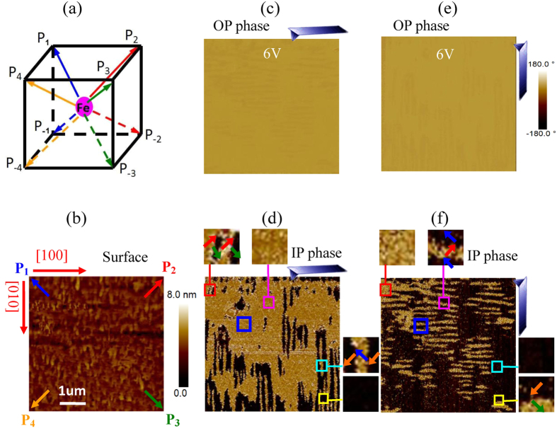
The μm-size striped domains with 71o boundaries are introduced in the fully polarized 70 nm BiFeO3 film on the (0 0 1) SrTiO3 single-crystal substrate with La0.67Sr0.33MnO3 buffer layer. There are eight different polarization orientations along the four diagonal lines of a BiFeO3 crystal cell in Fig. 1a8,9. In the (0 0 1) BiFeO3 film, the four upward polarizations (P1, P2, P3 and P4) are toward the surface and the four downward polarizations (P−1, P−2, P−3 and P−4) are toward the La0.67Sr0.33MnO3 buffered layer. There is a nano-scale smooth surface in the 5 × 5 μm2 region of the as-grown BiFeO3 film (Fig. 1b). After the as-grown film was polarized by 6 V from the La0.67Sr0.33MnO3 layer (Fig. 1c,e), P1, P2, P3 or P4 were introduced (Fig. 1d,f). The tip can probe the polarization to be perpendicular to its cantilever in our system. P1 and P2 are yellow and P3 and P4 are black when the cantilever is along [1 0 0] in Fig. 1d, and P2 and P3 are yellow and P1 and P4 are black when the cantilever is along [0 1 0] in Fig. 1f13. It is found that striped domains with P2–P3, P3–P4 or P4–P1 periodic structure predominate. In previous studies, the polarization orientations and the domain sizes of BiFeO3 film were successfully tailored by the static epitaxial strain from the film substrate8,9,10,11,12,13. Although thermal or epitaxial strain did not introduce striped domains in our as-grown film, it stabilized the periodic domain structure after the film was fully polarized.
Figure 1. The domain structure of BiFeO3 film.
(a) The sketch of eight possible polarization orientations in a BiFeO3 crystal cell; (b) the surface morphology, (c) out-of-plane (OP) and (d) in-plane (IP) phase images of the 6 V polarized regions; (e) the OP and (f ) IP phase images of the same region observed with a 90o-rotated tip, where the [1 0 0] and [0 1 0] are crystal orientations, some domains with P1, P2, P3 and P4 are marked in (d) and (f ), respectively.
Electrical switching of ferroelectric polarization
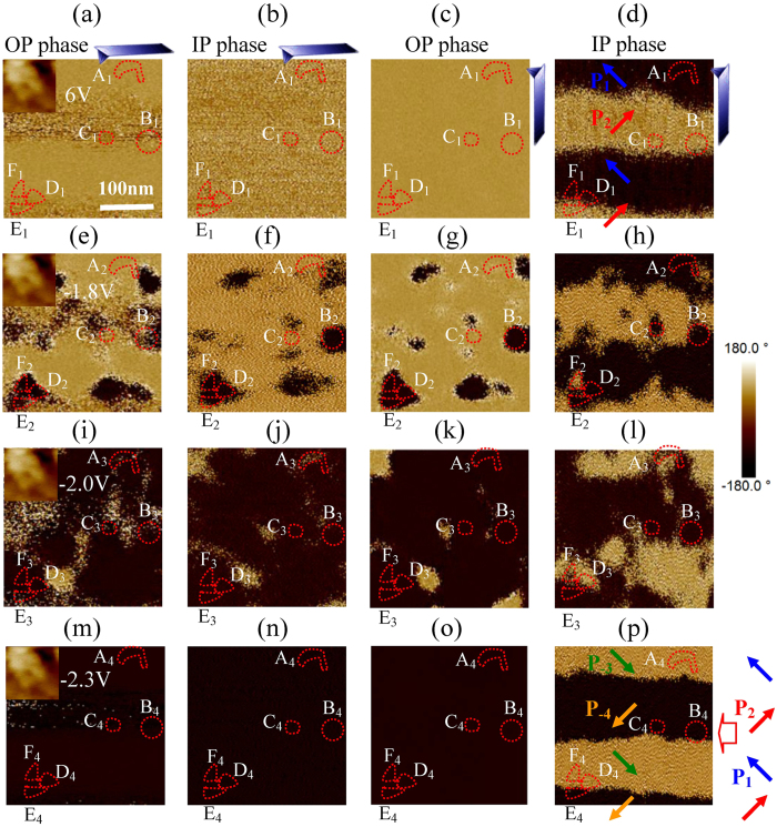
New domains nucleate preferentially at the previous domain boundaries under a negative bias. The P1–P2 striped domains in the blue square of Fig. 1d–f are amplified and shown in Fig. 2a–d, where the inset is the corresponding surface morphology. There is a single domain in A, B, C, D, E and F regions, respectively. After the surface was scanned by a tip with −1.8 V bias, some new domains (e.g. B2, C2, D2, E2 and F2) appeared at the previous P1–P2 domain boundaries in Fig. 2e–h5. To our surprise, P1–P2 boundaries were blurry, because the polarization was not unique at domain boundaries within the resolution of PFM. For the −2 V polarized region, the upward polarization becomes downward in over 94% regions (Fig. 2i–l). Many μm-size yellow and black domains do not have clear color contrast with each other, because they decompose to small or even nano-size domains due to various polarization switching routes in neighboring regions (e.g. A3)7. Nanodomains are beyond the resolution of PFM and thus they show a brown color instead of the yellow or black seen in horizontal PFM images. The brown color did not come from the instrumental phase offset since the μm-size domains outside the −2 V polarized region still show yellow or black colors.
Figure 2. The electrical switching of ferroelectric polarization.
The OP and IP phase images of the 6 V polarized area observed by a PFM tip with (a,b) 0o and (c,d) 90o rotations, and these phase images of the same area after it was polarized by (e–h) −1.8 V, (i–l) −2 V and (m–p) −2.3 V, where the inset is surface morphology and six independent regions are marked with A,B,C,D,E and F.
The nano-size domains assembled to μm-size P−3/P−4 domains in the region of most previous striped domains when the poling field is larger than the coercive field (EC). After the film was polarized by −2.3 V again, P−3 and P−4 domains commonly exist in the regions of previous P1 and P2 domains (Fig. 2m–p), partially because the strain of P1–P2 striped domains is the same as that of the P−3–P−4 striped domains. That is to say, the P1→P−3 or P2→P−4 180o switching was realized through two steps (e.g. A2(P1)→A3(P−1)→A4(P−3)) here.
Mechanical switching of ferroelectric polarization
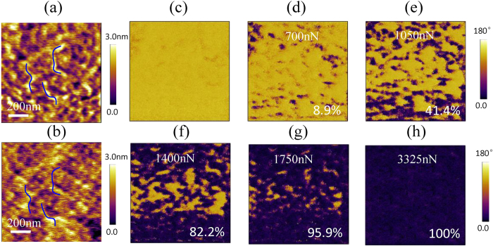
A mechanical force applied by the PFM tip can switch ferroelectric polarization through the flexoelectric effect14,15,16,17. The surface morphology of our BiFeO3 film is nm-scale smooth, as shown in Fig. 3a, which is important for the PFM tip to generate a large stress on the BiFeO3 film without inducing irreversible plastic damage. The mechanical switching has been investigated by scanning the 1 × 1 μm2 area of the upward polarized domain with the 30-nm-diameter tip under an incremental mechanical force from 700 to 3325 nN, with a corresponding change in the applied stress from 0.25 to 1.18 GPa. Note that, although the maximum local stress is very large, it is still well below the threshold for irreversible plastic damage of the BiFeO3 surface (Fig. 3b). In the tip-stressed BiFeO3 film, a strain gradient develops mainly along the film’s normal, which introduces an asymmetric distribution of lattice deformation underneath the tip. This gives rise to a local electric field, i.e., the flexoelectric field, pointing to the substrate due to the flexoelectric effect18,19,20. The flexoelectric field is given by Ef =(f/ε)·(∂e/∂z), where f is the flexoelectric tensor, ε is the dielectric constant of the BiFeO3 thin film, e is the strain due to the mechanical force of PFM tip, and z is the spatial coordinate along the film’s normal14,15,16,17. The Ef increases with the increase of mechanical force, which breaks the symmetry in the ferroelectric potential of BiFeO3 and makes the upward polarizations energetically unfavorable18, 19, 20.
Figure 3. The mechanical switching of ferroelectric polarization.
The surface morphology (a) before and (b) after it was scanned by the PFM tip with 3325 nN mechanical force. The OP phases image of the same region after it was scanned by the PFM tip with a force of (c) 140 nN, (d) 700 nN, (e) 1050 nN, (f ) 1400 nN, (g) 1750 nN and (h) 3325 nN, where the percent is the ratio of area with downward polarization.
The mechanical switching of polarization and its domain evolution are similar to those of the electrical switching. There is just upward polarization in the original image (Fig. 3c). When the mechanical force is 700 nN, the downward polarized domain starts to nucleate and then propagates. After the force of 700 nN, 1050 nN, 1400 nN, 1750 nN and 3325 nN had been applied by the PFM tip, the downward polarized domains were induced in the 8.9% (Fig. 3d), 41.4% (Fig. 3e), 82.2% (Fig. 3f), 95.9% (Fig. 3g) and 100% (Fig. 3h) region of total area, respectively. The downward polarized domains were stable after the sample had been kept for two days in air, which suggests the complete switching of polarization in 70 nm film.
Discussion
Table 1 summarizes the possible routes of polarization switching triggered by an electric field (Fig. 2) or a mechanical force (Fig. 4). According to previous phase-field calculation, direct 180o polarization switching is not kinetically favorable because of the high activation barrier. Instead, the ferroelastic relaxation-mediated 180o switching path through 71o switching is expected21. Not only the polarization direction but also the direction of lattice distortion changes at 109° and 71° ferroelastic domain walls7,8,9,10. There is an easy magnetization plane for the orientation of the magnetic moments, which is always perpendicular to the ferroelectric polarization orientation. Either 109o or 71o polarization switching changes the orientation of the easy magnetization plane8,9,10. The realization of permanent magnetoelectric coupling in the single-phase BiFeO3 requires ferroelastic (71o, 109o) rather than ferroelectric (180o) domain switching21,22,23. That is to say, there may exist transient magnetoelectric coupling during the 180o polarization switching which is commonly composed of a 71o and a 109o polarization switching. In the intermediate stage of the 180o switching, there are several possible polarization orientations, and thus tiny domains are the most popular.
Table 1. Different polarization switching routes of BiFeO3 film under an electric field or a mechanical force.
| Electrical switching of polarization | ||||||
|---|---|---|---|---|---|---|
| A1(P1) (6 V) | = | A2(P1) |  |
A3(P−1) |  |
A4(P−3)(−2.3 V) |
| B1(P2)(6V) |  |
B2(P−4) | ≈ | B3(P−4) | = | B4(P−4)(−2.3 V) |
| C1(P2) (6 V) |  |
C2(P1) |  |
C3(P−4) | = | C4(P−4)(−2.3 V) |
| D1(P1)(6 V) |  |
D2(P−4) |  |
D3(P−3) | ≈ | D4(P−3)(−2.3 V) |
| E1(P2) (6 V) |  |
E2(P−4) | = | E3(P−4) | = | E4(P−4)(−2.3 V) |
| F1(P1) (6 V) |  |
F2(P−3) | ≈ | F3(P−3) | ≈ | F4(P−3)(−2.3 V) |
| Mechanical switching of polarization | ||||||
| G1(P1)(6V) |  |
G2(P−2) | ≈ | G3(P−2) |  |
G4(P−3)(1330 nN) |
| H1(P1)(6V) |  |
H2(P−2) | ≈ | H3(P−2) |  |
H4(P−3)(1330 nN) |
| I1(P1)(6V) | = | I2(P1) | ≈ | I3 (P1) |  |
I4(P−3)(1330 nN) |
| J1 (P4)(6V) |  |
J2(P−3) |  |
J3(P−2) | = | J4(P−2)(1330 nN) |
| K1(P1)(6V) |  |
K2(P−2) | ≈ | K3(P−2) |  |
K4(P−3)(1330 nN) |
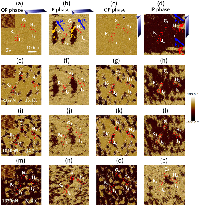
Figure 4. The mechanical switching of ferroelectric polarization.
The OP and IP phase images of the 6 V polarized area observed by a PFM tip with (a,b) 0o and (c,d) 90o rotations, and the images of the same area after it was polarized by a mechanical force of (e–h) 875 nN, (i–l) 1050 nN, (m–p) 1330 nN, where the inset is the surface morphology, the five independent regions are marked with G,H,I,J and K, and the percent is the ratio of area with downward polarization.
Although the ~70 nm BiFeO3 film shows a much higher coercive field than that of the BaTiO3 film with similar thickness, its polarization was completely switched by a 3325 nN force. Recently, the epitaxial strain from substrate is widely used to tailor domain type or introduce self-polarization in BiFeO38,9,10,11,12,13. Besides, flexoelectricity also plays an important role in the self-polarized direction in BiFeO3 film and ceramics24,25. Nowadays the inhomogeneous strain introduced by PFM tip can switch ferroelectric polarization of the 70 nm BiFeO3 film and the mechanical switching of polarization is the same as the electrical switching. In addition to polarization switching, the tetragonal-rhombohedral phase transition can be introduced through an electric field or a mechanical force in a >50 nm BiFeO3 film with morphotropic phase boundaries on LaAlO3 substrate11,13,26,27. Although the mechanical force from AFM tip is large enough to trigger these polarization switching and phase transition indeed, other factors such as the epitaxial strain from substrate or the built-in electric field near the film interface may play an important role on these changes. This work is important for more applications since it is much easier to prepare and measure the ~70 nm ferroelectric films than the ~5 nm films14,15,16,17.
The domain evolution due to the mechanical switching is similar to that of the electrical switching. The domain evolution under a mechanical force is clearly observed and its polarization switching routes are identified accordingly. The μm-size P1–P4 and P1–P2 striped domains were formed in Fig. 4a–d. There is a single domain in G(P1), H(P1), I(P1), J(P4) and K(P1) regions, respectively. With the mechanical force increasing gradually from 875 to 1330 nN, new tiny domains nucleate at the boundaries of μm-size domains, and then more and more μm-size domains decompose to nm-size domains due to different polarization switching routes (Fig. 4e–p). Polarization of G, H, J and K first has 71o/109o switching and then 109o/71o switching21,22,23, e.g. G1(P1)→ G2(P−2) → G4(P−3) and J1(P4)→ J2(P−3) → J3(P−2). As a result, the 180o polarization switching was achieved with two steps. The routes of these regions are shown in Table 1.
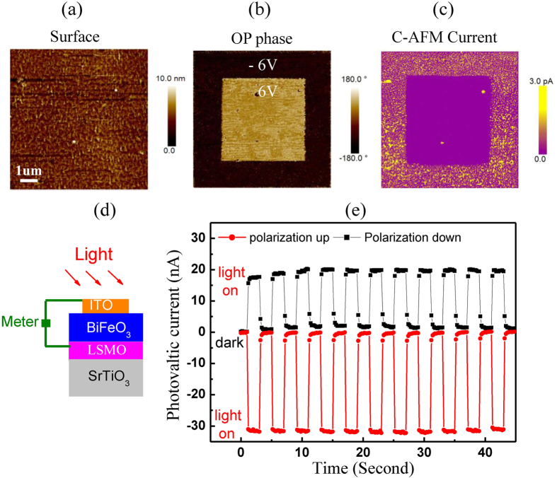
Ferroelectric polarization can be nondestructively read-out without another polarization switching in our BiFeO3 film. The regions with upward and downward polarization were polarized by a ±6 V tip bias (Fig. 5a–b), and these regions were characterized by a conductive AFM tip with 1 V bias. It is noted that 1 V is much lower than the coercive voltage (VC) of ±2.3 V which corresponds to the EC of 38 kV/mm. The region with downward polarization shows much higher current than the region with upward polarization (Fig. 5c). Therefore the leakage current under a <VC voltage can read out information in a nondestructive way28,29. Oxygen vacancies are typical n-type dopant in BiFeO3 film. There is a depletion layer at the interface between the p-type La0.67Sr0.33MnO3 interlayer and the n-type BiFeO3 film. The downward polarization increases the leakage current through narrowing the depletion layer at the La0.67Sr0.33MnO3/BiFeO3 interface while the upward polarization decreases the leakage current through widening the depletion layer28,29,30,31. Furthermore, we measured the intrinsic photovoltaic effect of the BiFeO3 films with 300-μm-diameter transparent ITO electrodes which was illuminated by a visible light (~100 mW/cm2) (Fig. 5d). The short-circuit current (Isc) direction is always opposite to the polarization direction in Fig. 5e. The Isc after downward poling was 20 nA, whereas the Isc after upward poling was about −30 nA31. The Isc can be switched by polarization flipping. In addition, there is no obvious photocurrent degradation when the Isc was measured during eleven on-and-off cycles of the illumination light. Such good retention and high stability over multiple cycles suggest that the polarization status can be nondestructively read out through the analysis of Isc.
Figure 5. The ferroelectric polarization is nondestructively read out.
(a) The surface morphology, (b) the OP phase image and (c) the conductive image with 1 V bias after the film were polarized by 6 V and −6 V bias, respectively. (d) The sketch of photovoltaic measurement. (e) The photovoltaic current of BiFeO3 with upward or downward polarization when light illuminates the BiFeO3 surface or not.
In summary, the electrical switching of polarization in the ~70 nm epitaxial BiFeO3 film is similar to that of mechanical switching. The 180o polarization switching is commonly completed with two steps. At first, a μm-size domain decomposes to nano-size domains due to the 71o/109o/180o polarization switching, and then they merge to a μm-size domain due to the other 109o/71o/0o switching. Most importantly, the upward polarization can be switched downward with a mechanical force even in the ~70 nm BiFeO3 film, and then the polarization status can be nondestructively read out through the analysis of constant current.
Methods
Thin film fabrication
BiFeO3 (~70 nm) epitaxial films and La0.67Sr0.33MnO3 (~70 nm) buffer layers were grown on commercial (0 0 1) SrTiO3 substrates using pulsed laser deposition (PLD) at 630 oC and 16 Pa oxygen pressure inside the chamber. The wavelength, frequency and energy per pulse of KrF excimer laser were 248 nm, 1 Hz and 60 mJ. After that, the as-grown samples were kept at 630 oC and 1000 Pa oxygen pressure for 30 minutes in order to reduce oxygen vacancies, and then they were cooled down at 5 oC per minute to 300 oC. For photovoltaic measurement, indium tin oxide (ITO, In2O3:SnO2=9:1) top electrodes with 300 μm diameter were grown on the BiFeO3 film surface at room temperature using PLD.
Electrical measurements
The surface morphology, out-of-plane (OP) phase, in-plane (IP) phase and amplitude images were studied by using the commercial atomic force microscope (AFM, Bruker multimode 8 or Asylum Research Cypher) with a piezoelectric force microscopy (PFM) mode. The conductive AFM tip is either Bruker MESP-RC with 35 nm tip radius or Nanoworld EFM with 30 nm tip radius. The spatially resolved conductance image was measured with the conductive AFM at 1 V sample bias (Bruker multimode 8). The photovoltaic current is measured with a Keithley 2635 multimeter when the film surface was illuminated by the light of a xenon lamp at 100 mW/cm2.
Additional Information
How to cite this article: Chen, L. et al. Electrical and mechanical switching of ferroelectric polarization in the 70 nm BiFeO3 film. Sci. Rep. 6, 19092; doi: 10.1038/srep19092 (2016).
Acknowledgments
The work is supported by the National Natural Science Foundation of China (11134004, 11234005, 51472118 and 11374320).
Footnotes
Author Contributions G.L.Y conceived the experiments, L.F.C. and W. T. X. grew the films, L.F.C and Z.H.C. performed the conductive AFM and PFM measurements. G.L.Y., X.J.M., J.M.L. and Z.G.L. analyzed data and then co-wrote the manuscript.
References
- Jung J. H. et al. Lead-free NaNbO3 nanowires for a high output piezoelectric nanogenerator. ACS Nano 5, 10041–10046 (2011). [DOI] [PubMed] [Google Scholar]
- Chang C., Tran V. H., Wang J., Fuh Y.-K. & Lin L. Direct-write piezoelectric polymeric nanogenerator with high energy conversion efficiency. Nano Lett. 10, 726–731 (2010). [DOI] [PubMed] [Google Scholar]
- Lee C.-H. et al. Exploiting dimensionality and defect mitigation to create tunable microwave dielectrics. Nature 502, 532–536 (2013). [DOI] [PubMed] [Google Scholar]
- Scott J. F. & Paz de Araujo C. A. Ferroelectric memories. Science 246, 1400–1405 (1989). [DOI] [PubMed] [Google Scholar]
- Shin Y. H., Grinberg I., Chen I. W. & Rappe A. M. Nucleation and growth mechanism of ferroelectric domain-wall motion. Nature 449, 881–884 (2007). [DOI] [PubMed] [Google Scholar]
- Wang J. et al. Epitaxial BiFeO3 Multiferroic Thin Film Heterostructures. Science 299, 1719–1722 (2003). [DOI] [PubMed] [Google Scholar]
- Shafer P. et al. Planar electrode piezoelectric force microscopy to study electric polarization switching in BiFeO3. Appl. Phys. Lett. 90, 202909 (2007). [Google Scholar]
- Chu Y.-H. et al. Electric-field control of local ferromagnetism using a magnetoelectric multiferroic. Nat Mater 7, 478–482 (2008). [DOI] [PubMed] [Google Scholar]
- Zhao T. et al. Electrical control of antiferromagnetic domains in multiferroic BiFeO3 films at room temperature. Nat Mater 5, 823–829 (2006). [DOI] [PubMed] [Google Scholar]
- Chu Y.-H. et al. Domain Control in Multiferroic BiFeO3 through Substrate Vicinality Adv. Mater. 19, 2662–2666 (2007). [Google Scholar]
- Zeches R. J. et al. A Strain-Driven Morphotropic Phase Boundary in BiFeO3. Science 326, 977–980 (2009). [DOI] [PubMed] [Google Scholar]
- Cruz M. P. et al. Strain Control of Domain-Wall Stability in Epitaxial BiFeO3 (110) Films. Phys. Rev. Lett. 99, 217601 (2007). [DOI] [PubMed] [Google Scholar]
- You L. et al. Characterization and Manipulation of Mixed Phase Nanodomains in Highly Strained BiFeO3 Thin Films. ACS Nano 6, 5388–5394 (2012). [DOI] [PubMed] [Google Scholar]
- Lu H. et al. Mechanical Writing of Ferroelectric Polarization. Science 336, 59–61 (2012). [DOI] [PubMed] [Google Scholar]
- Lu H. et al. Mechanically-Induced Resistive Switching in Ferroelectric Tunnel Junctions. Nano Lett. 12, 6289–6292 (2012). [DOI] [PubMed] [Google Scholar]
- Guo E. J., Roth R., Das S. & Dorr K. Strain induced low mechanical switching force in ultrathin PbZr0.2Ti0.8O3 films. Appl. Phys. Lett. 105, 012903 (2014). [Google Scholar]
- Baek S. H. et al. Ferroelastic switching for nanoscale non-volatile magnetoelectric devices. Nat Mater 9, 309–314 (2010). [DOI] [PubMed] [Google Scholar]
- Baek S. H. et al. The Nature of Polarization Fatigue in BiFeO3. Adv. Mater. 23, 1621–1625 (2011). [DOI] [PubMed] [Google Scholar]
- Balke N. et al. Deterministic control of ferroelastic switching in multiferroic materials. Nature Nanotechnology 4, 868–875 (2009). [DOI] [PubMed] [Google Scholar]
- Wen Z. et al. Mechanical switching of ferroelectric polarization in ultrathin BaTiO3 films: The effects of epitaxial strain. Appl. Phys. Lett. 104, 042907 (2014). [Google Scholar]
- Zubko P., Catalan G., Buckley A., Welche P. R. L. & Scott J. F. Strain-gradient-induced polarization in SrTiO3 single crystals, Phys. Rev. Lett. 99, 167601 (2007). [DOI] [PubMed] [Google Scholar]
- Catalan G., Noheda B., McAneney J., Sinnamon L. J. & Gregg J. M. Strain gradients in epitaxial ferroelectrics, Phys. Rev. B 72, 020102 (2005). [Google Scholar]
- Catalan G., Sinnamon L. J. & Gregg J. M. The effect of flexoelectricity on the dielectric properties of inhomogeneously strained ferroelectric thin films, J. Phys. Conder. Matter. 16, 2253–2264 (2004). [Google Scholar]
- Chen X. M. et al. Temperature Gradient Introduced Ferroelectric Self-Poling in BiFeO3 Ceramics. J. Amer. Cerm. Soc. 96, 3788–3792 (2013). [Google Scholar]
- Jeon B. C. et al. Flexoelectric Effect in the Reversal of Self-Polarization and Associated Changes in the Electronic Functional Properties of BiFeO3 Thin Films. Adv. Mater. 25, 5643–5649 (2013). [DOI] [PubMed] [Google Scholar]
- Heo Y., Jang B. K., Kim S. J. & Seidel, J. Nanoscale mechanical softening of morphotropic BiFeO3, Adv. Mater. 26, 7568–7572 (2015). [DOI] [PubMed] [Google Scholar]
- Li Y. J. et al. Mechnical switching of nanoscale multiferroic phase boundaries, Adv. Funct. Mater. 25, 3405–3413 (2015). [Google Scholar]
- Jiang A. Q. et al. A Resistive Memory in Semiconducting BiFeO3 Thin-Film Capacitors. Adv. Mater. 23, 1277–1281 (2011). [DOI] [PubMed] [Google Scholar]
- Yuan G. L. & Wang J. L. Evidences for the depletion region induced by the polarization of ferroelectric semiconductors. Appl. Phys. Lett. 95, 252904 (2009). [Google Scholar]
- Choi T., Lee S., Choi Y. J., Kiryukhin V. & Cheong S.-W. Switchable Ferroelectric Diode and Photovoltaic Effect in BiFeO3. Science 324, 63–66 (2009). [DOI] [PubMed] [Google Scholar]
- Yi H. T., Choi T., Choi S. G., Oh Y. S. & Cheong S.-W. Mechanism of the Switchable Photovoltaic Effect in Ferroelectric BiFeO3. Adv. Mater. 23, 3403–3407 (2011). [DOI] [PubMed] [Google Scholar]


