Abstract
This work presents characterization studies of thick silicon double-sided strip detectors for a high-resolution small-animal SPECT. The dimension of these detectors is 60 mm × 60 mm × 1 mm. There are 1024 strips on each side that give the coordinates of the photon interaction, with each strip processed by a separate ASIC channel. Our measurement shows that intrinsic spatial resolution equivalent to the 59 µm strip pitch is attainable. Good flood uniformity can be achieved by proper setting of a 4-bit DAC in each ASIC channel to remove trigger threshold variations. This is particularly important for triggering at low energies. The thick silicon DSSD shows high potential for small-animal SPECT imaging.
I. Introduction
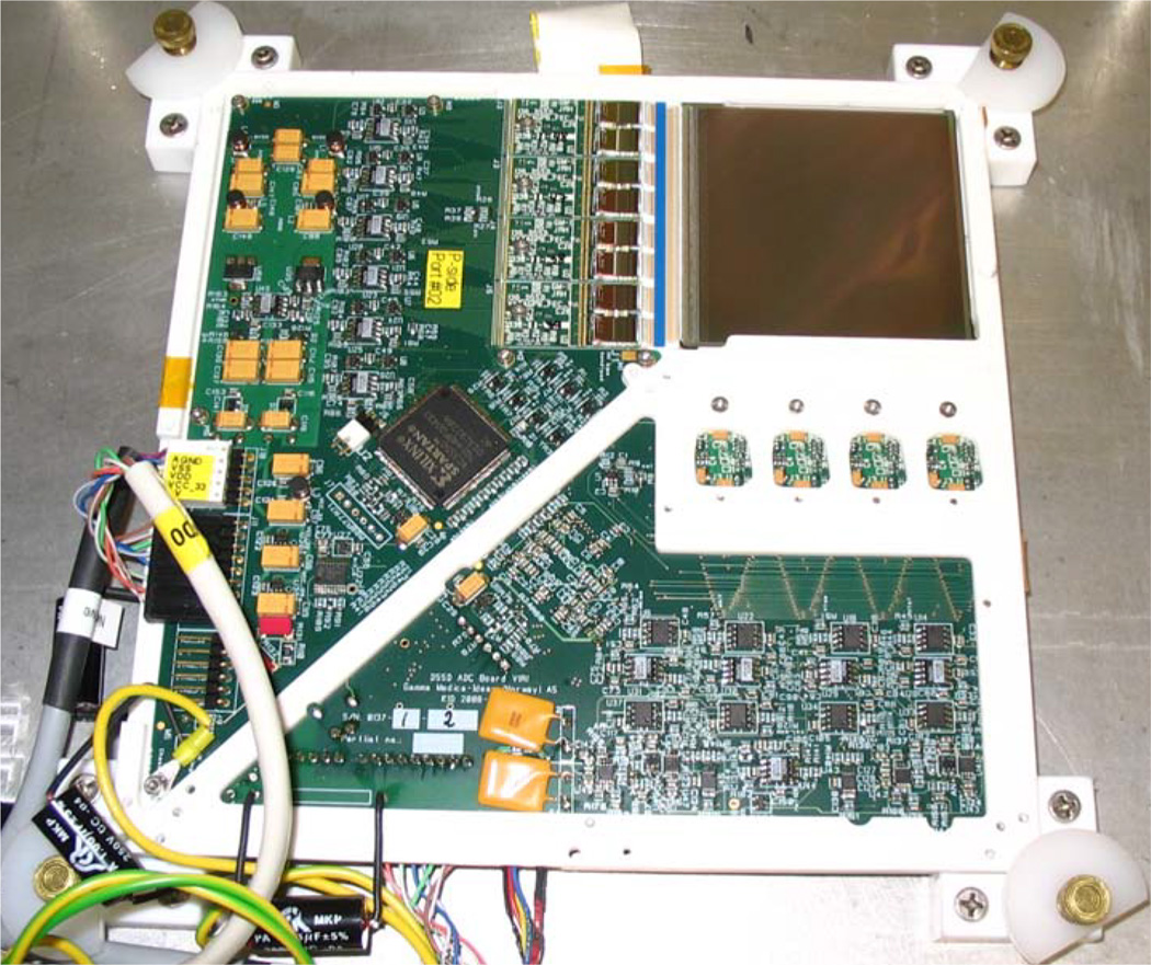
We previously [1] demonstrated some preliminary performance characteristics of a new generation of silicon double-sided strip detectors (DSSDs) with a thickness of one mm, an active area of 60 mm × 60 mm and an improved ASIC. Fig. 1 shows the detector board. This detector is intended for use in combination with a multiple-pinhole aperture for a high-resolution SPECT system, SiliSPECT [2], designed for imaging at low energies, such as those from the decay of 125I.
Fig. 1.
Image of the detector board with silicon DSSD, located on the top right corner of the board, and the readout electronics. The silicon DSSD is 60 mm × 60 mm × 1 mm.
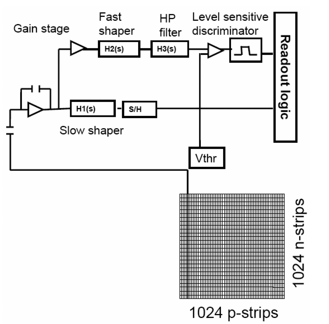
There are 1024 strips on each detector side. The strips on the P(junction)-side are orthogonal to the N(ohmic)-side. The coordinates of the photon interaction are given by the orthogonal pair of strips with the largest induced signal. The readout of the silicon DSSD is accomplished using a custom-designed 128-channel ASIC, the VATAGP6, manufactured by Gamma Medica-Ideas. Each strip is wire-bonded to a separate ASIC channel. Therefore, the readout requires 8 ASICs on each detector side for a total of 16 ASICs per detector to process the 2048 independent channels. By monitoring this comparatively modest number of channels, we are able to read out 1,048,576 virtual pixels or resolution elements. The ASIC provides each channel with a preamplifier, shaper, sample and hold, fast shaper and comparator circuitry (Fig. 2).
Fig. 2.
Silicon DSSD and front-end electronics scheme
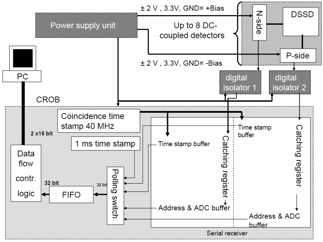
Fig. 3. shows the basic schematic of the data acquisition block diagram. All communication between the front-end and the back-end electronics, the coincidence readout board (CROB), is digital. Since the DC voltages for operating the front-end electronics are referenced with respect to the bias on their corresponding detector side, digital isolators are used to decouple the bias voltage from the signals. Each arriving event is given a time stamp on the CROB based on a 40 MHz clock. This time stamp is referred to as the coincidence time stamp, and is used to determine coincident triggers on the two detector sides. An additional, slower clock writes a time word every millisecond into the event stream, and is used for real-time tracking of count rates. This feature also provides us the option of doing dynamic imaging. The readout system features list mode acquisition of independently triggered N and P strips for off-line coincidence processing. The events are sent as two 16 bit packets/words from the CROB, and are written to a binary file. By reading back and combining the packet format definitions with bit masking, one can identify and filter out the different packet types in off-line analysis. There are three types of packets (i.e. two 16 bit words) on the data-stream. An event packet indicates the address, ADC value and the module number (detector side) and is always followed by a coincidence packet that indicates the timestamp and module number. An additional time stamp packet is always sent out at a fixed rate. Since the event and coincidence packets come in pairs, the coincident packets are used to identify coincident events. In addition to single channel readout, nearest-neighbor readout is available. The leader event flag in the event packets marks the first, i.e. center channel, in sparse readout. Events from the same module that arrive afterwards without the leader event flag set are neighbors.
Fig. 3.
Block diagram of the data-acquisition system. Up to four detector cards can be supported with a single power supply and CROB.
II. Detector Performance
A. Intrinsic detector resolution
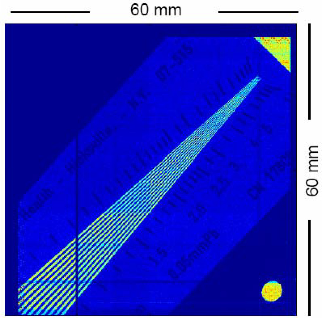
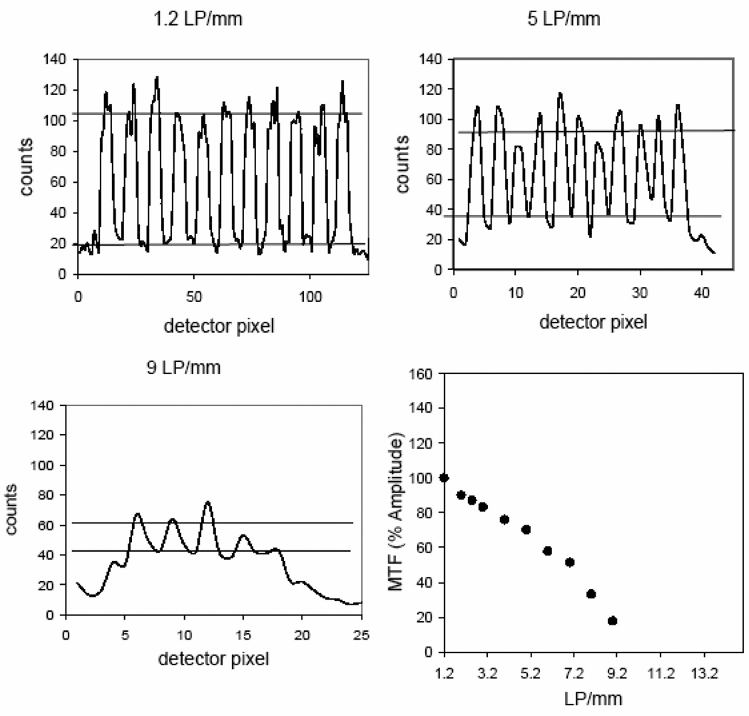
The 59 µm detector strip pitch suggests a high intrinsic resolution. This was measured experimentally by placing a line-pair phantom diagonally on the silicon detector and acquiring the phantom’s projection image with a 125I flood source. Line pair (LP) phantoms are commonly used for high resolution x-ray imaging systems, and the phantom we used had spatial frequencies up to 10 line pairs per mm. Fig. 4 shows the projection image of the phantom on the detector. Fig. 5 shows multiple profiles that were taken from the projection image at different spatial frequencies. From these image profiles, we obtained the modulation transfer function (MTF), which dropped to 1/10th of its maximum at 9.5 LP/mm (55 µm).
Fig. 4.
Projection image of the LP phantom on SiliSPECT exposed to 125I flood source.
Fig. 5.
Change of modulation of the phantom image with increasing spatial frequency and the obtained modulation transfer function.
B. Acquisition with stacked detectors
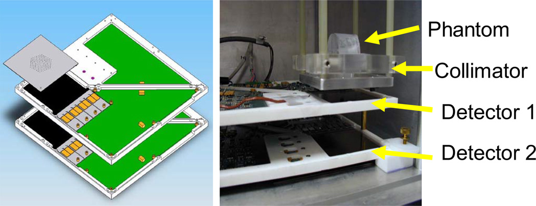
The detection efficiency of a one millimeter silicon detector is 39% for low energy photons of around 30keV. To offset this moderate efficiency we stack two silicon DSSDs in each camera head (Fig. 6), increasing the total detection efficiency while at the same time collecting pinhole projection data at two different magnifications.
Fig. 6.
Stacked detector acquisition with multi-pinhole collimator and a phantom.
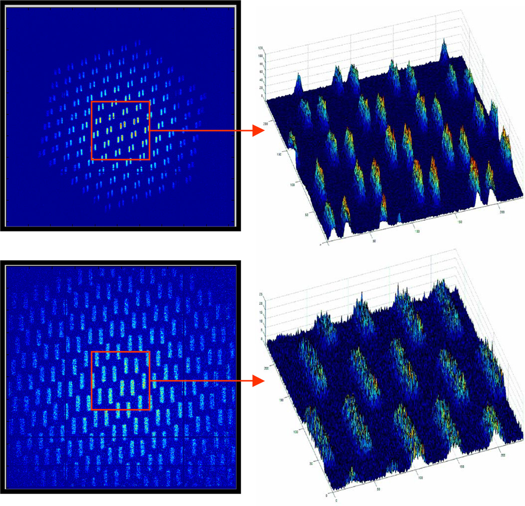
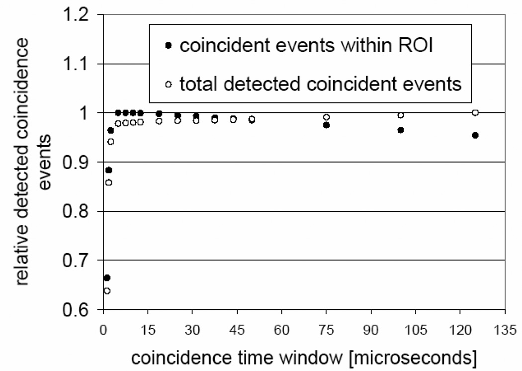
Fig. 7 shows multi-pinhole projections on the front and back detectors using an off-line sorting algorithm to assign coincident events between orthogonal strips. The optimal coincidence timing window was selected based on image analysis methods for this particular acquisition with 63 µCi activity from a pair of brachytherapy seeds and a multi-pinhole collimator system [2]. The collimator consisted of 127 pinholes, each 250 µm in diameter, that were laser-drilled through the tungsten. The pinholes were cylindrical in shape and tilted toward a common focal point at a distance of 30 mm away from the collimator surface. We used segmentation masks to determine the number of coincident events within regions of interest (ROI) in the projection image. Fig. 8 shows the relative number of coincident events in the ROI and the total number of detected coincident events across the entire detector surface for different time windows in the coincidence sorting algorithm. The optimal window was found to be between 5 and 10 µsec.
Fig. 7.
Projection images with stacked detector acquisition and multi-pinhole collimator.
Fig. 8.
The total detected coincident events on the detector increases as expected with a wider coincidence time window. However, the detected events within the ROI start to decline at larger time windows due to mismatch of coincident triggers.
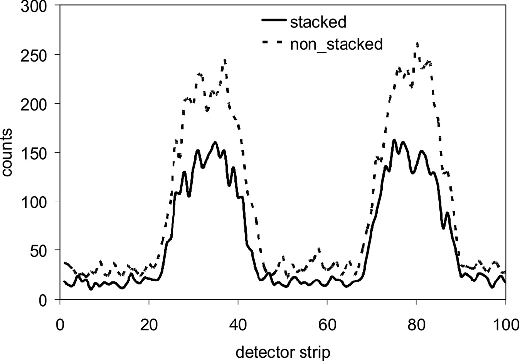
Fig. 9 shows two line profiles from the back detector projection that were acquired with and without the presence of the front detector. We compared these profiles with respect to their signal-to-background ratios and full width at half maxima and did not detect any significant changes in the profiles in the presence of the front detector other than the expected lower count total due to attenuation of photons in the first detector. From this we conclude that inter-detector scatter does not degrade the imaging performance.
Fig. 9.
Comparison of projection profiles on the back detector with and without the front detector present.
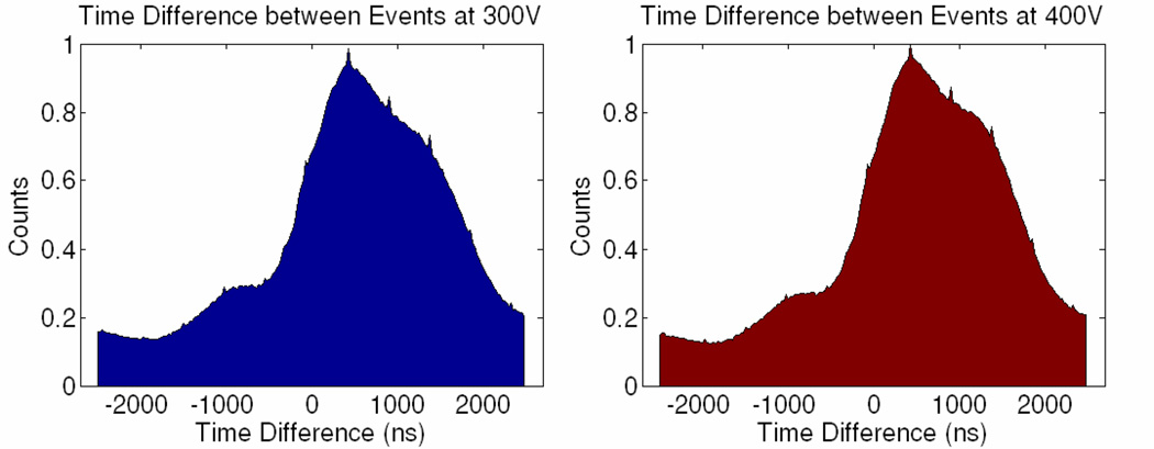
We also collected a larger amount of data from all the detector strips and histogrammed their time difference at 300 V and 400 V detector bias (the depletion voltage is between 90–150 V for these detectors). These histograms are shown in Fig. 10.
Fig. 10.
Histograms of time differences collected from all detector strips at two different bias voltages.
The time stamps are generated after the completion of the readout cycle when the digitized signals are transferred to the CROB. This contributes to the poor timing resolution seen from the timing histograms since the time-stamping does not follow immediately after the occurrence of the trigger signal. This could be problematic at higher data frequency, leading to improper association of events from the two detector sides. However, the expected count rates in our SPECT applications should not be negatively impacted by the relatively poor timing resolution. We attribute the unusual and non-symmetric shape of the timing histograms to the time differences among different combinations of ASIC pairs. We are investigating the origins of these time differences and ways to correct them.
C. Trigger Uniformity at low energy
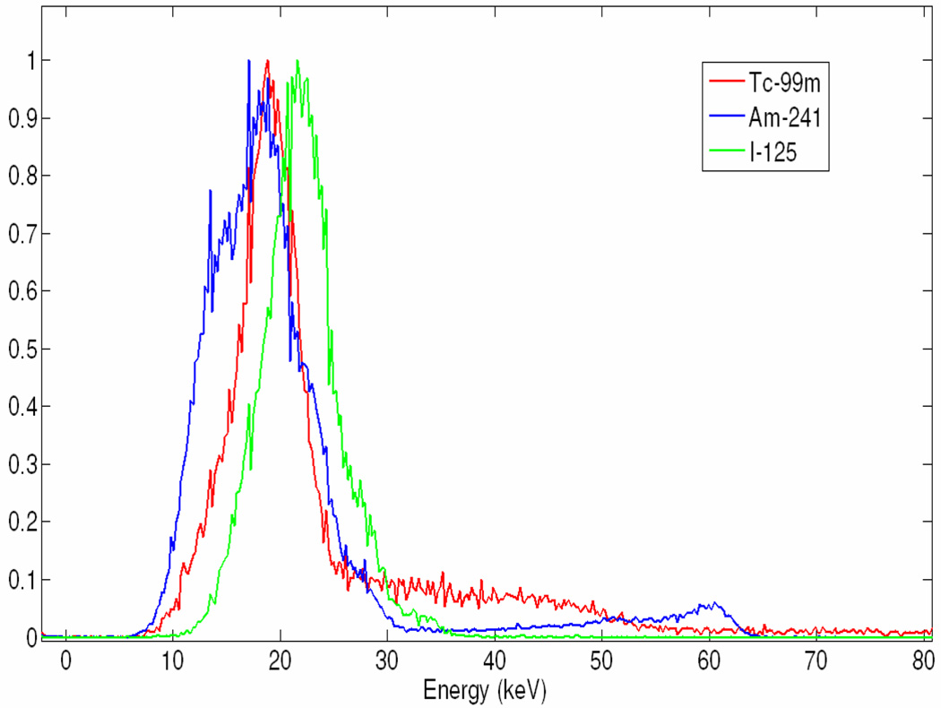
In conventional SPECT imaging, good energy resolution is an important detector characteristic for setting optimal energy windows and suppressing scattered photons. With SiliSPECT, our imaging applications are limited to lower energy photons such as those from the decay of 125I (27.2–35.5 keV). Here, the rejection of Compton scattered photons is not feasible with energy windowing due to the small energy loss even at large scattering angles. The energy threshold should ideally be set just above the noise level to collect every photon that interacts in silicon. Fig. 11 shows the energy spectrum of Tc-99m, Am-241, I-125 acquired with a single P-side strip.
Fig. 11.
The energy spectra of Tc-99m, Am-241, I-125 acquired with a single p-side strip. The full width at half maximum of the 18 keV peak of Tc-99m was 5.2 keV.
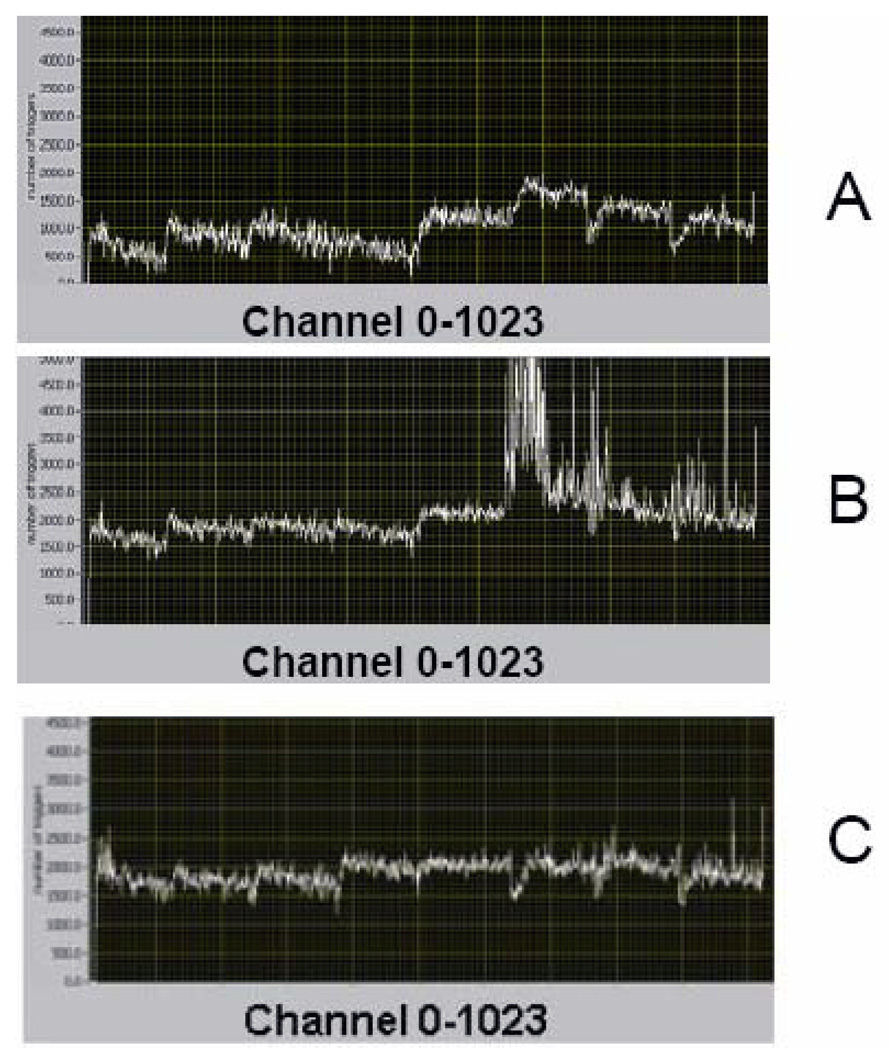
One main requirement for achieving better detection efficiency at low energies without triggering on noise is the capability of adjusting the trigger threshold for individual channels that have different gains and offsets to achieve uniform triggering. For this purpose, the new ASIC has 4-bit DACs associated with each channel for making individual fine adjustments to the main threshold applied to each ASIC. We have implemented software routines that can iteratively adjust all the channels in a way that generated currents are always compensated and uniform trigger response is achieved across the detector (Fig. 12).
Fig. 12.
Trigger histogram across 1024 channels from one detector side. Non-uniform triggering (A) at high channel threshold without adjusted DACs. Increase of noise triggers (B) at low channel threshold without adjusted DACs. More uniform triggering with less noise triggers (C) at low channel threshold with adjusted channel DACs.
D. Charge sharing effects
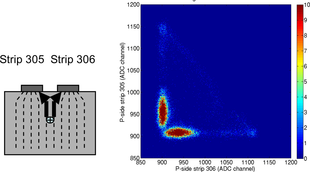
It is important to evaluate the fraction of events where the induced charges in silicon are collected by more than one strip. This charge sharing effect is responsible for the accumulation of events that have lower energies than the actual energy deposited through the photon interaction. It also makes efficient triggering for low energy imaging more difficult due to the increased chances of acquiring noise triggers due to the need to set thresholds sufficiently low to reliably trigger on events in which not all of the charge is collected on a single strip. For incident photon energies at around 30 keV we intend to set the trigger threshold near 15 keV for an optimal collection of all events. We evaluated the charge sharing effect by including the nearest neighbors in the data readout (Fig. 13).
Fig. 13.
Plot of strip 306 versus lower neighboring strip 305 for Am-241 spectrum. The ~60 keV peak is broadly shared between the strips.
III. Summary And Discussion
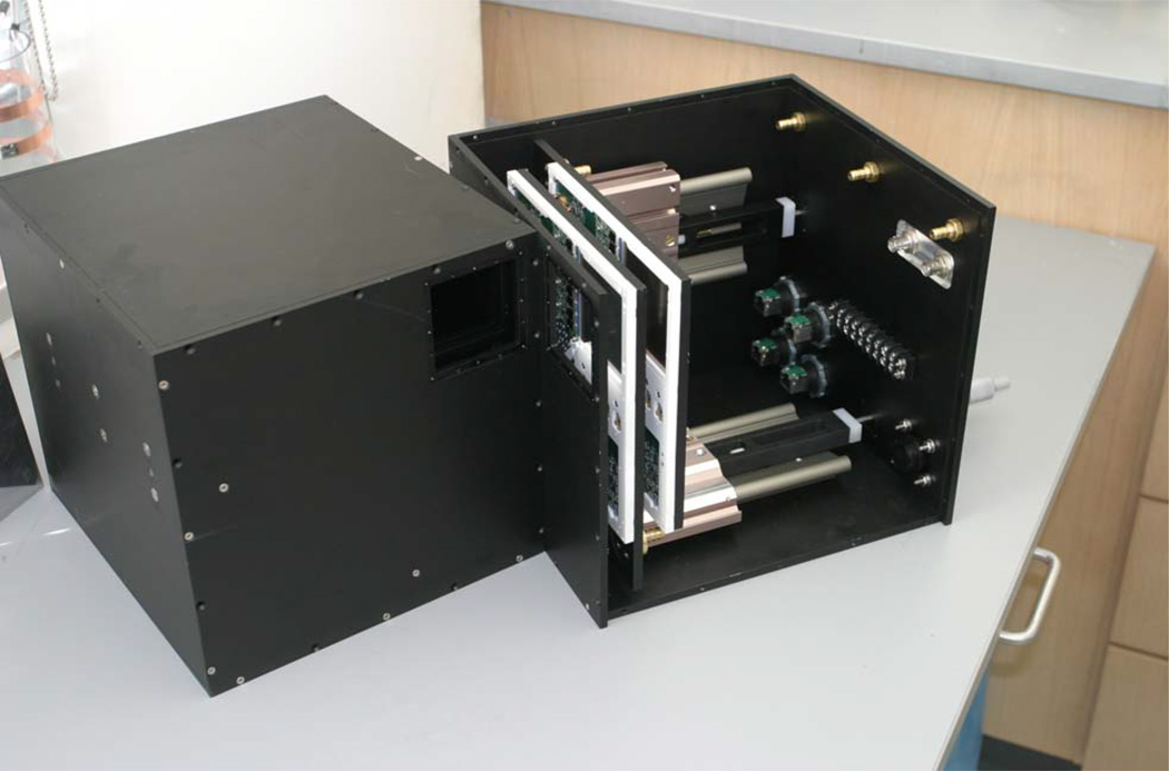
This paper reported some initial characterization studies of silicon double-sided strip detectors to evaluate them for low-energy SPECT imaging. The results on the intrinsic detector resolution indicated an excellent resolution matching the detector strip pitch and making these devises suitable for applications that require high resolution such as mouse brain imaging. A global timing window in vicinity of 5 µsec gave the optimal number of correctly assigned coincident events for typical experimental count rates. The poor timing resolution is thought to be dominated by the way the time stamps are generated in the data acquisition process, but should be sufficient for the count rates that we expect to see in SPECT imaging. We have shown the feasibility of stacked detector acquisition with one millimeter thick silicon detectors, and that the projection images on the back detectors were not degraded by the presence of the front detectors. We were able to make significant improvements in achieving uniform trigger response across a large number of channels at low energies with minimal numbers of noise triggers. Our detector studies suggest that these types of silicon DSSDs have good potential for high-resolution SPECT imaging. Fig. 14 shows the image of our dual-headed and stationary SPECT camera based on these detectors that is currently under construction.
Fig. 14.
SiliSPECT is a dual-headed SPECT with two silicon DSSDs stacked on each camera head.
Acknowledgments
This work was supported by the NIH/NIBB grants R33 EB000776, P41EB002035 and a Career Award at the Scientific Interface from the Burroughs Welcome Fund.
Contributor Information
Sepideh Shokouhi, Vanderbilt University, Nashville, TN, USA.
Benjamin S. McDonald, Vanderbilt University, Nashville, TN, USA
Heather L. Durko, University of Arizona, Center for Gamma-Ray Imaging and the College of Optical Sciences, Tucson, AZ, USA
Mark A. Fritz, Vanderbilt University, Nashville, TN, USA
Lars R. Furenlid, University of Arizona, Center for Gamma-Ray Imaging and the College of Optical Sciences, Tucson, AZ, USA
Todd E. Peterson, Vanderbilt University, Nashville, TN, USA
References
- 1.Shokouhi S, Durko HL, Fritz MA, Furenlid LR, Peterson TE. Thick Silicon Strip Detectors for Small-Animal SPECT Imaging. IEEE Nucl. Sci. Symp. Conference record. 2006;6:3562–3566. [Google Scholar]
- 2.Shokouhi S, Fritz MA, McDonald BS, Wilson DW, Durko HL, Furenlid LR, Wilson Donald W, Peterson TE. A Silicon SPECT System for Molecular Imaging of the Mouse brain; IEEE, NSS-MIC conference; 2007. [DOI] [PMC free article] [PubMed] [Google Scholar]


