Abstract
The emergence of metallic conduction in layered dichalcogenide semiconductor materials by chemical doping is one of key issues for two-dimensional (2D) materials engineering. At present, doping methods for layered dichalcogenide materials have been limited to an ion intercalation between layer units or electrostatic carrier doping by electrical bias owing to the absence of appropriate substitutional dopant for increasing the carrier concentration. Here, we report the occurrence of metallic conduction in the layered dichalcogenide of SnSe2 by the direct Se-site doping with Cl as a shallow electron donor. The total carrier concentration up to ~1020 cm−3 is achieved by Cl substitutional doping, resulting in the improved conductivity value of ~170 S·cm−1 from ~1.7 S·cm−1 for non-doped SnSe2. When the carrier concentration exceeds ~1019 cm−3, the conduction mechanism is changed from hopping to degenerate conduction, exhibiting metal-insulator transition behavior. Detailed band structure calculation reveals that the hybridized s-p orbital from Sn 5s and Se 4p states is responsible for the degenerate metallic conduction in electron-doped SnSe2.
Two dimensional (2D) materials have recently been intensively investigated due to its unique electronic and/or optical properties1,2,3,4,5,6,7. Since the remarkable properties of graphene have initiated the research, other 2D materials with layered structure are also emerged as new counterparts to exhibit striking physical properties under the 2D confined systems1,2,3. Layered dichalcogenides are one of the representative materials drawing great attention from the fact that they can be easily prepared as a form of high quality nanosheet by mechanical and/or chemical exfoliation techniques as graphene did2,4.
As a practical engineering method to modulate 2D material properties, doping is an important technique especially for controlling electrical characteristics. Until now, the doping methods for 2D materials have been tried mainly by electrostatic carrier doping introduced by the electrical bias through an dielectric barrier5,6, or insertion of interstitial intercalants between the layer units which are weakly bonded each other by Van der Waals interaction7,8,9. In particular, for the case of layered dichalcogenides, striking carrier transport characteristics can be provoked by effective carrier doping5,6,8,9, but direct substitutional doping has been rarely reported due to the absence of adequate substitutional dopant to the best of our knowledge10.
In this study, we report the emergence of metallic conduction in layered dichalcogenide of SnSe2 achieved by direct Se-site doping with Cl atoms. Substitutional Cl dopant on Se-site worked well as a shallow electron donor to increase carrier concentration (ne) up to ~1020 cm−3, and the transition from semiconductor to metallic state was observed when ne exceeded critical limit (~1019 cm−3). Based on the electronic structure calculation, it was clarified that the hybridization between largely spread Sn 5s and Se 4p orbital is the origin of degenerate conduction in Cl-doped SnSe2.
Results and Discussion
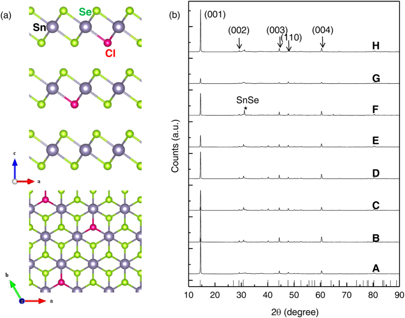
Figure 1(a) schematically illustrates the crystalline structure of SnSe2 as characterized by the powder X-ray diffraction (PXRD) results in figure 1(b). SnSe2 has a hexagonal layered structure (P-3m1 space group) with lattice parameters of a = 3.81 Å and c = 6.13 Å, which agree well with those reported in literature11. Fig. 1(b) shows the PXRD results with increasing Cl dopant ratio introduced during SnSe2 synthesis. The doped samples were named from A to H with increasing dopant content as listed in Table 1. No observable impurity compound associated with Cl dopant was detected except for small amount of SnSe phase in the sample F. The lattice parameters of the samples were calculated from the PXRD patterns and also listed in Table 1. They are almost identical within 0.1% variation for all samples. Similar lattice parameters of the samples are attributed to the fact that Se2− (1.98 Å) has similar ionic radius to Cl− (1.81 Å), supporting that Cl dopants are not located on the inter-layer space as intercalants, but on the Se site as substitutional atoms for Se2− to minimize the lattice deformation12. The theoretical prediction for formation energies of probable defect states also indicates that Cl substitution to Se-site is the most stable compared to other defect candidates. (Figure S1 in the supplementary information).
Figure 1. Structural characterizations of Cl-doped SnSe2.
(a) Schematics of crystal structure of Cl-doped SnSe2 along b- (upper) and c-axis (lower). (b) The patterns of powder X-ray diffraction from various amount of Cl-doped SnSe2 samples [A: undoped (ne = 7.2 × 1017 cm−3), B–H: doped samples with increasing Cl doping ratio from B (ne = 5.1 × 1018 cm−3) to H (ne = 8.6 × 1019 cm−3)]. Reference peak positions of SnSe2 are displayed at the bottom of the graph. Representative lattice planes are indicated and SnSe impurity phase is marked with arrows and asterisk, respectively.
Table 1. Nominal amount of Cl contents and lattice parameters extracted from PXRD patterns of respective Cl-doped SnSe2 samples.
| sample | Nominal amount of Cl content | Lattice parameter |
|
|---|---|---|---|
| (x) | a (Å) | c (Å) | |
| A | 0 | 3.81043 (35) | 6.13279 (37) |
| B | 0.002 | 3.81085 (20) | 6.13322 (20) |
| C | 0.004 | 3.81086 (20) | 6.13408 (30) |
| D | 0.006 | 3.81126 (18) | 6.13321 (23) |
| E | 0.010 | 3.81097 (20) | 6.13392 (29) |
| F | 0.020 | 3.81055 (28) | 6.13306 (32) |
| G | 0.030 | 3.80848 (33) | 6.13364 (59) |
| H | 0.040 | 3.80934 (34) | 6.13173 (36) |
To more strongly reveal the Cl dopant substitution on Se-site in SnSe2 samples, we performed X-ray photoemission spectroscopy (XPS) as well as Raman spectroscopy with non-doped (A of x = 0) and the most heavily doped sample (H of x = 0.04). As shown in figure 2(a), characteristic Cl 2p core level peak at 199.05 eV was observed with sample H while sample A did not show any Cl related one. From the fact that the measured core level corresponds well with Cl– state which is almost identical to the Cl 2p position in the form of CdCl213, it indicates that the Cl dopant exists as Cl– state which could serve well as an electron donor if it substitutes on Se2− site. Figure 2(b) displays the Raman spectroscopy results with the same samples. With sample H, we could observe not only the downshift but also the peak broadening occurred for A1g mode compared to those from sample A14. It strongly evidences that Cl dopant well substitutes on Se-site as decreasing the force constant in SnSe2 as reported in other substitutionally doped materials15,16,17.
Figure 2. XPS and Raman spectroscopy.
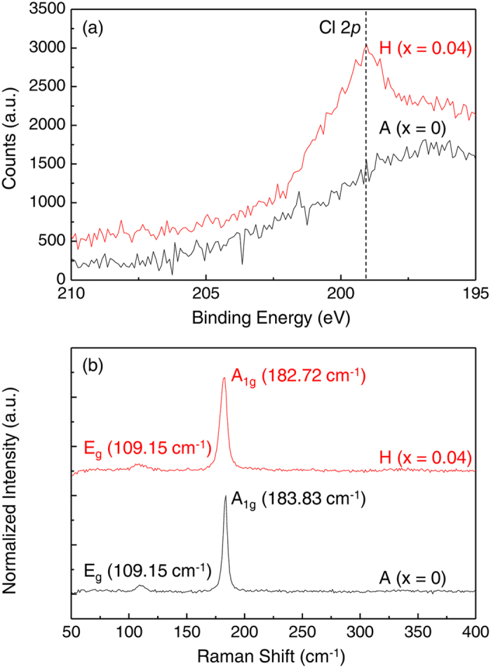
(a) X-ray photoemission and (b) Raman spectroscopy results for sample A (x = 0, non-doped SnSe2) and sample H (x = 0.04) Dashed line in Fig. 2(a) remarks the characteristic Cl- peak position.
Figure 3(a–c) shows the temperature (T ) dependence of conductivity (σ), ne, and mobility (μ), respectively for Cl-doped SnSe2 samples, extracted from the measurement of four point-probe resistivity and Hall coefficient. As shown in Fig. 3(a), σ exhibits thermally activated behavior from A to C sample, while the trend changes to degenerate conduction for sample D to H. Hall-effect measurement reveals that all SnSe2 samples are n-type and their ne value increases up to 8.6 × 1019 cm−3 (H sample with nominal Cl content, x of 0.04) with the maximum σ value of ~170 S·cm−1 at 300 K as Cl doping ratio increases as shown in Fig. 3(b). (The ne values of the sample E, F and G are located in-between those of the sample D and H (refer to Fig. 4), showing same electrical behavior and removed for brevity). It proves that Cl dopants act as electron donors to SnSe2 and that Cl− is successfully substituted on Se2− site simultaneously supported by XPS and Raman results. (See Fig. 2) It should be noted that ne becomes T independent when degenerate conduction occurs as is the case with sample D and H. It indicates that the Fermi level (EF) exceeds the conduction band edge of SnSe2 as ne increases over 1019 cm−3 18. T dependence of μ was deduced from the relation of σ = eneμ, where e is the charge of electron and presented in Fig. 3(c)19. When ne is less than 1019 cm−3, μ is limited by lattice vibration scattering at high T region, while limiting scattering mechanism changes to ionized impurity scattering at low T region as also displayed in figure S2(b) in supplementary information20. (The transition point is observed at about 100 K.) With the samples with high ne over 1019 cm−3, μ value keeps increasing as T decreases and saturates at specific values, indicating that μ of the samples is governed dominantly by lattice vibration scattering in whole T region, as is the case with typical metals19. Experimental results of electrical transport strongly support the emergence of metallic states from layered SnSe2 semiconductor by Cl substitutional doping on Se-site.
Figure 3. Electron transport properties of Cl-doped SnSe2.
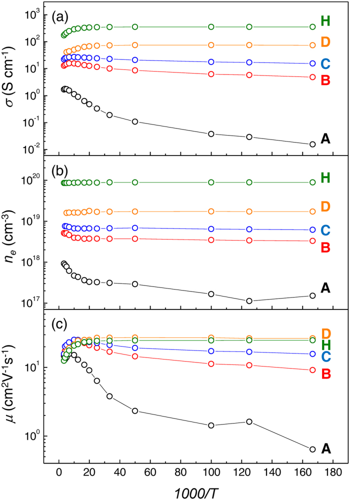
Temperature dependence of (a) electrical conductivity, (b) carrier concentration and (c) mobility of Cl-doped SnSe2 samples.
Figure 4. Disorder parameters of Cl-doped SnSe2.
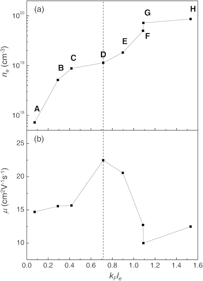
Disorder parameter (kFle) dependences of (a) carrier concentration and (b) mobility of Cl-doped SnSe2 samples at 300 K. Dashed line points out the critical point [(kFle)c = 0.71] where metal-insulator transition occurs.
To investigate the origin of semiconductor to metal transition in Cl-doped SnSe2, we estimate the disorder parameter, kFle, based on the Ioffe-Regel criterion, which can be determined by6,21,22,23,
 |
where kF is Fermi wave number, le is electron mean free path, and ħ is Plank’s constant divided by 2π. In figure 4(a), the relation between kFle and ne at 300K is plotted based on equation (1). From the fact that degenerate conduction occurs when ne exceeds 1.13 × 1019 cm−3 as observed in Fig. 3, we can obtain the critical value of (kFle)c as 0.71 where the metal-insulator transition occurs. (Note that the metal-insulator transition point can also be confirmed by estimating w(0) from the mathematical function of w(T) = d(lnσ)/d(lnT) as shown in figure S324). As shown in figure 4(b), μ increases with increasing kFle when kFle < (kFle)c, while it starts decreasing when kFle > (kFle)c. As Pearson and Bardeen have proposed, donor ionization energy (Ed) should decreases with increasing ne for the doped semiconductor with a substitutional dopant atom due to the decrease of average potential energy of electrons25. Ed can be calculated from the slope of ln(ne) versus 1/T plot (Refer to figure S2(a) in supplementary information) for the case of kFle < (kFle)c based on the relation below19,
 |
where Nc is the effective density of states at conduction band edge, Nd is donor concentration, and kB is the Boltzmann constant. The values are estimated as 13.97, 6.95, and 3.77 meV for ne of 7 × 10¹⁷, 5 × 10¹⁸, and 9 × 1018 cm−3 at 300 K, respectively. It strongly suggests that the increase of μ with ne increment (for kFle < (kFle)c) mainly originates from enhanced le with reduced Ed which is deeply associated with trap energy levels of the scatterers in the semiconductor regime25. On the other hand, when ne exceeds the critical value, (kFle)c, Cl dopants starts to act as scattering centers, then μ starts decreasing due to ionized impurity scattering. As a consequence, it can be concluded that metallic transition of conduction mechanism for SnSe2 is primarily due to sufficient electron concentration and long electron mean free path achieved from shallow Ed level.
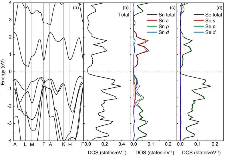
Figure 5(a)–(d) describe the calculated band structure and density of states (DOS) profiles of un-doped SnSe2 based on density functional theory (DFT). As shown in Fig. 5(a), EF is set to be zero in the energy scale. The conduction band minimum (CBM) and valence band maximum (VBM) are located at L-M and H-Γ path, respectively, indicating the indirect band-gap semiconductor nature which agrees well with our experimental results for non-doped SnSe2. Since the structural parameters are almost identical regardless of Cl doping ratio as confirmed by PXRD results (see Table 1), it is reasonable to assume the rigid band behavior with raised EF upon CBM for an electron-doped SnSe2 system. As ne increases, EF shifts upward until it meets CBM, and degenerate conduction should occur based on the CBM state, as are the case with typical heavily doped degenerate semiconductors18,26. As observed from the results of total and projected DOS in Fig. 5(b)–(d), the total DOS mainly consists of Sn 5s and Se 4p orbitals with similar contributions, indicating that the metallic conduction of electron-doped SnSe2 originates from the hybridized orbital states between Sn 5s and Se 4p orbital. It is worthwhile to note that (kFle)c value of 0.71 for electron-doped SnSe2 is close to those of conducting oxide materials showing largely spread orbital conduction such as In 5s ((kFle)c = 0.1 ~ 0.3 for In2O3, In-Ga-Zn-O and In-Zn-O), but much smaller than the reported value of other layered transition metal dichalcogenide. ((kFle)c = 2.5 for electron-doped MoS2)6,22,23. It strongly suggests that electron pathways in SnSe2 would be dispersed well, compared to localized electrons in other layered chalcogenide materials, due to effective overlap of delocalized large Sn 5s orbital as observed in In-based conducting oxide group. Therefore, metallic conduction of Cl-doped SnSe2 could be attributed to a large number of electrons supplied by efficient substitutional doping and their de-localization behavior originated from Sn 5s orbital.
Figure 5. Electronic structure of SnSe2.
(a) Calculated band structure of SnSe2. Fermi energy level is taken as origin. (b–d) Density of states profiles from total, Sn and Se contribution, respectively.
Conclusions
In summary, we successfully synthesized metallic layered SnSe2 from original semiconducting state by direct substitutional doping of Cl atoms. Doped Cl atoms on Se-site acted well as shallow donors to introduce high ne up to ~1020 cm−3, changing conduction mechanism to degenerate conduction from thermally activated conduction of undoped SnSe2. Detailed analysis of carrier transport mechanism and calculation of band structure confirm that metallic transport in electron-doped SnSe2 originates from highly dispersive Sn 5s orbital which is hybridized with Se 4p state. We anticipate that the engineering of conductivity from semiconducting to metallic states by direct chemical doping can be used as key technology for practical applications of 2D layered dichalcogenide materials, as has been proven for Si-based technology.
Methods
Sample synthesis
To synthesize polycrystalline SnSe2 samples doped with Cl, we mixed stoichiometric amount of Sn and anhydrous SnCl2 powders: (2−x)Sn + xSnCl2 → 2SnClx, and then melted the mixtures in fused silica tubes at 250 °C for 24 hrs. (Detailed nominal x’s are listed in Table 1.) After the first reaction was finished, stoichiometric Se grains were added to synthesize the final compound of Cl-doped SnSe2: 2SnClx + 2(2−x)Se → 2SnSe2−xClx, followed by the second annealing process in fused silica tubes at 600 °C for 48 hrs. To improve homogeneity, the synthesized samples were ground into powder form in an agate mortar and re-annealed by repetition of the process described above. Densification of all synthesized samples was conducted with spark plasma sintering (SPS) equipment at 500 °C for 10 min under a pressure of 70 MPa, which resulted in higher densities than 95% of theoretical values.
Structural and electrical analysis
The crystalline phases of the fabricated samples were identified by PXRD using a Bruker diffractometer model D8 ADVANCE (Cu Kα). To measure the electrical properties of polycrystalline Cl-doped SnSe2 pellets, electrical contacts in the four point-probe and Hall bar geometries were made by applying Ag paste onto the samples. The four point-probe resistivity and Hall coefficient were measured in the temperature range of 6–300 K using Physical Property Measurement System (PPMS, Quantum Design).
Spectroscopic analysis
The XPS was carried out using focused monochromatized Al Kα radiation (1486.6 eV). Raman spectra were measured by confocal Raman spectrometer with 488 nm wavelength excitation.
Electronic structure calculations
To investigate electronic structure of SnSe2, first principle calculations implemented in the Vienna ab initio simulation program (VASP) code were performed. The generalized gradient approximation (GGA) in Perdew-Burke-Ernzerhof (PBE) functional form and the projected augmented plane-wave (PAW) method were employed, which is distinct from previous calculation methods27,28,29. The plane-wave basis-sets with 240 eV cut-off were used. And valence electron states of 4d105s25p2 and 4s24p4 were considered for Sn and Se atoms, respectively. The convergence threshold was set to be 10−2 eV·Å−1 and 10−4 eV for force and energy minimization, respectively. The experimental lattice constants of a = 3.81 Å and c = 6.13 Å for SnSe2 were used.
Additional Information
How to cite this article: Il Kim, S. et al. Metallic conduction induced by direct anion site doping in layered SnSe2. Sci. Rep. 6, 19733; doi: 10.1038/srep19733 (2016).
Supplementary Material
Acknowledgments
This work was supported by the National Research Foundation of Korea (NRF) grant funded by the Korea government (Ministry of Science, ICT & Future Planning)(No.2015M3D1A1070639) and research funds of Kunsan National University.
Footnotes
Author Contributions K.L., I.H. and Y.S. conceived the study. K.L. designed the experiments. S.I.K., S.H., S.Y.K., D.W.J., K.S.M., H.J.P. and K.L. synthesized the samples. J.H.K. performed and analysed the PXRD experiments. D.J.Y. carried out the XPS measurement. S.I.K. and K.L. analysed the Raman spectroscopy results. Y.J.C. and K.L. measured the electrical transport properties. W.J.L. and Y.H.C. performed and analysed the DFT calculations. S.I.K., S.H., S.Y.K., K.L. and Y.S. co-wrote the manuscript. All the authors discussed the results and commented on the manuscript.
References
- Novoselov K. S. et al. A roadmap for graphene. Nature, 490, 192–200 (2012). [DOI] [PubMed] [Google Scholar]
- Wang Q. H., Kalantar-Zadeh K., Kis A., Coleman J. N. & Strano M. S. Electronic and optoelectronics of two-dimensional transition metal dichalcogenides. Nature Nanotechnol. 7, 699–712 (2012). [DOI] [PubMed] [Google Scholar]
- Lee K., Kim S. W., Toda Y., Matsuishi S. & Hosono H. Dicalcium nitride as atwo-dimensional electride with an anionic electron layer. Nature, 494, 336–340 (2013). [DOI] [PubMed] [Google Scholar]
- Coleman J. N. et al. Two-dimensional nanosheets produced by liquid exfoliation of layered materials. Science, 331, 568–571 (2011). [DOI] [PubMed] [Google Scholar]
- Ye J. T. et al. Superconducting dome in a gate-tuned band insulator. Science, 338, 1193–1196 (2012). [DOI] [PubMed] [Google Scholar]
- Radisavljevic B. & Kis A. Mobility engineering and a metal–insulator transition in monolayer MoS2. Nature Mater. 12, 815–820 (2013). [DOI] [PubMed] [Google Scholar]
- Khrapach I. et al. Novel highly conductive and transparent graphene-based conductors. Adv. Mater. 24, 2844–2849 (2012). [DOI] [PMC free article] [PubMed] [Google Scholar]
- Hermann A. M., Somoano R., Hadek V. & Rembaum A. Electrical resistivity of intercalated molybdenum disulfide. Solid State Commun. 13, 1065–1068 (1973). [Google Scholar]
- Formstone C. A., Kurmoo M., FizGerald E. T., Cox P. A. & O’Hare D. Single-crystal conductivity study of the tin dichalcogenide SnS2–xSex intercalated with cobaltocene. J. Mater. Chem. 1, 51–57 (1991). [Google Scholar]
- Xia C. et al. The characteristics of n- and p-type dopants in SnS2 monolayer nanosheets. Phys. Chem. Chem. Phys. 16, 19674–19680 (2014). [DOI] [PubMed] [Google Scholar]
- Palosz B. & Salje E. Lattice parameters and spontaneous strain in AX2 polytypes: CdI2, PbI2, SnS2 and SnSe2. J. Appl. Cryst. 22, 622–623 (1989). [Google Scholar]
- Atkins P., Overton T., Rourke J., Weller M. & Armstron F. Inorganic Chemistry 5th ed. (Oxford University Press, 2010). [Google Scholar]
- Nefedov V. I. X-ray photoelectron spectra of halogens in coordination compounds. J. Electron. Spectrosc. 12, 459–476 (1977). [Google Scholar]
- Mead D. G. & Irwin J. C. Raman spectra of SnS2 and SnSe2. Solid State Commun. 20, 885–887 (1976). [Google Scholar]
- Nickel N. H., Lengsfeld P. & Siever I. Raman spectroscopy of heavily doped polycrystalline silicon thin films. Phys. Rev. B 61, 15558–15561 (2000). [Google Scholar]
- Maciel I. O. et al. Boron, nitrogen and phosphorous substitutionally doped single-wall carbon nanotubes studied by resonance Raman spectroscopy. Phys. Status Solidi B 246, 2432–2435 (2009). [Google Scholar]
- Lv R. et al. Nitrogen-doped graphene: beyond single substitution and enhanced molecular sensing. Sci. Rep. 2, 586; doi: 10.1038/srep00586 (2012). [DOI] [PMC free article] [PubMed] [Google Scholar]
- K. Nomura et al. Carrier transport in transparent oxide semiconductor with intrinsic structural randomness probed using single-crystalline InGaO3(ZnO)5 films. Appl. Phys. Lett. 85, 1993–1995 (2004). [Google Scholar]
- Kasap S. O. Principles of Electronic Materials and Devices 2nd ed. (McGraw-Hill, 2002). [Google Scholar]
- Gowers J. P. & Lee P. A. Mobility of electrons in SnS2 single crystals. Solid State Commun. 8, 1447–1449 (1970). [Google Scholar]
- Ioffe A. F. & Regel A. R. Progress in Semiconductors, (Heywood, 1960). [Google Scholar]
- Makise K. et al. Relationship between variable range hopping transport and carrier density of amorphous In2O3–10 wt. % ZnO thin films. J. Appl. Phys. 112, 033716 (2012). [Google Scholar]
- Makise K. et al. Metal-insulator transitions in IZO, IGZO, and ITZO films. J. Appl. Phys. 116, 153703 (2014). [Google Scholar]
- Graham M. R., Adkins C. J., Behar H. & Rosenbaum R. Experimental study of the Ioffe-Regal criterion for amorphous indium oxide films. J. Phys.:Condens. Matter 10, 809–819 (1998). [Google Scholar]
- Pearson G. L. & Bardeen J. Electrical properties of pure silicon and silicon alloys containing boron and phosphorus. Phys. Rev. 75, 865 (1949). [Google Scholar]
- Rich D. H., Samsavar A., Miller T., Leibsle F. M. & Chiang T. C. Degenerate doping and conduction-band properties of Si studied by synchrotron photoemission of Sb/Si(001). Phys. Rev. B, 40, 3469 (1989). [DOI] [PubMed] [Google Scholar]
- He X. & Shen H. Ab initio calculations of band structure and thermophysical properties of SnS2 and SnSe2. Physica B, 407, 1146–1152 (2012). [Google Scholar]
- Murray R. B. & Williams R. H. Band structure and photoemission studies of SnS2 and SnSe2: II. Theoretical. J. Phys. C: Solid State Phys. 6, 3643–3651 (1973). [Google Scholar]
- Fong C. Y. & Cohen M. L. Electronic energy-band structure of SnS2 and SnSe2. Phys. Rev. B, 5, 3095–3101 (1972). [Google Scholar]
Associated Data
This section collects any data citations, data availability statements, or supplementary materials included in this article.


