Abstract
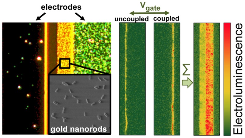
The ability to confine and manipulate light below the diffraction limit is a major goal of future multifunctional optoelectronic/plasmonic systems. Here, we demonstrate the design and realization of a tunable and localized electrical source of excitons coupled to surface plasmons based on a polymer light-emitting field-effect transistor (LEFET). Gold nanorods that are integrated into the channel support localized surface plasmons and serve as nanoantennas for enhanced electroluminescence. By precise spatial control of the near-infrared emission zone in the LEFET via the applied voltages the near-field coupling between electrically generated excitons and the nanorods can be turned on or off as visualized by a change of electroluminescence intensity. Numerical calculations and spectroscopic measurements corroborate significant local electroluminescence enhancement due to the high local density of photonic states in the vicinity of the gold nanorods. Importantly, the integration of plasmonic nanostructures hardly influences the electrical performance of the LEFETs, thus, highlighting their mutual compatibility in novel active plasmonic devices.
Keywords: surface plasmon polariton, organic semiconductor, field-effect transistor, electroluminescence, Purcell effect, active plasmonics
Optoelectronic devices based on charge density oscillations propagating along the metal–dielectric interface, that is, surface-plasmon polaritons (SPP), offer the necessary functionalities to bridge the gap between ultrafast photonics and high-density nanoelectronics. For practical applications of all-plasmonic circuitry, a full set of active and passive components is needed, including sources, detectors, and waveguiding structures for SPPs.1−5 Additional components should also possess the ability to modulate and route signals.6−10 Current technology has already overcome the problem of momentum mismatch between freely propagating far-field radiation and SPPs and offers near-field functionality for these components.11−16 Moreover, electrical excitation and detection in the near-field are possible. In combination with suppressed coupling to the far-field these components may enable completely dark plasmonic circuitry, where the signals are confined in the near-field, thus, limiting the overall losses. However, further improvements are still needed regarding performance and functionality.
In this context, we propose the light-emitting field-effect transistor (LEFET) as a planar electroluminescent device that can be used for controlled plasmonic coupling. As suggested by Falk et al., a field-effect transistor can be operated as a single plasmon detector with the ability for signal amplification.12 It is even more promising to operate it as a tunable source of confined electrically generated emitting dipoles (i.e., excitons) deliberately coupled to SPPs or not by simply changing the gate voltage. In an ambipolar LEFET, holes and electrons are injected into the channel from the source and drain electrodes, respectively, depending on the applied voltages.17 The charge accumulation layers meet within the channel resulting in a voltage-controlled p–n junction. Electron–hole recombination and thus light emission takes place in a narrow line, the recombination zone. Many different semiconductors can be used as the charge transport and emissive layer, for example quantum dot solids,18 single-walled carbon nanotubes,19,20 two-dimensional transition metal dichalcogenides,21 and organic semiconductors,22,23 thus, enabling emission from the visible to the near-IR. The position of the recombination zone can be changed deliberately along the entire channel length, depending on the gate and drain voltage. This enables the selective coupling of the narrow recombination zone to any nearby plasmonic components of interest with sub-μm precision. Furthermore, the number of excitons is directly and solely controlled by the drain current, because all injected holes and electrons must recombine when the recombination zone is located within the channel. The application of LEFETs for launching photons into dielectric waveguides was recently demonstrated.24 However, similar integration of metallic waveguides, for which better mode confinement is achievable (compared to the dielectric counterparts), has not yet been reported. Due to the complex set of parameters influencing the dynamics of charge carriers in LEFETs, it is an open question whether they can operate when metallic nanostructures are incorporated into or close to the semiconducting channel. As shown recently by Baeg et al.,25 metallic nanoparticles can increase charge carrier trapping via tunneling and may behave as a floating gate. Furthermore, metallic structures close to the active channel could alter the electric field distribution and thus modify charge carrier density.26
In this work we overcome these challenges and demonstrate successful integration of plasmonic nanoantennas into LEFETs and their efficient voltage-controlled coupling with electrically excited excitons. Colloidal gold nanorods (NRs) that support localized surface plasmons (LSP) are used as a model system where, due to the Purcell effect, the degree of coupling can be visualized and quantified. By tuning the applied voltages, the recombination zone is moved away or brought close to the gold NRs, thus, turning the coupling on or off. In addition to paving the way toward multifunctional plasmonic devices based on the LEFET design, the obtained physical insights may also help to develop more efficient electroluminescent devices.
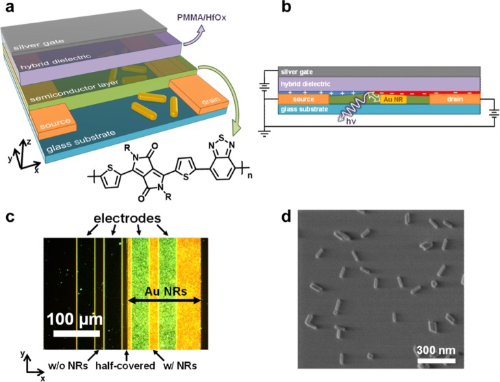
The device geometry and operation principle of a top-gated ambipolar LEFET are shown in Figure 1a and b, respectively. The device was fabricated on a glass substrate to facilitate optical access and consisted of doctor-bladed colloidal gold NRs covered by a 1 nm layer of AlOx for electrical insulation. The NRs were synthesized following a water-based approach and redispersed in tetrahydrofuran after ligand exchange (removed by oxygen plasma treatment in the device), as described elsewhere.27,28 Source-drain electrodes (2 nm Cr/30 nm Au) were patterned photolithographically and covered with 15 nm of a narrow bandgap semiconducting polymer (diketopyrrolopyrrole copolymer, DPPT-BT), followed by a high capacitance hybrid gate dielectric (11 nm poly(methyl methacrylate) and 38 nm HfOx)29 and a 35 nm silver gate (for device fabrication details, see Supporting Information).
Figure 1.
(a) Schematic geometry of a top-gated light-emitting field-effect transistor (LEFET) with one-half of the channel coated with gold nanorods (NRs) and (b) LEFET operation principle with recombination and emission zone (not to scale). (c) Dark-field microscopy image of LEFET under white-light illumination showing four electrodes and three channels: without, half-covered, and with gold NRs. (d) Scanning electron micrograph of a typical high density gold nanorod distribution prepared by doctor-blading of a colloidal nanorod dispersion.
Upon application of drain and gate voltage (the source is grounded), electrons and holes accumulate at the semiconductor–dielectric interface, as illustrated in Figure 1b. Since the nominal thickness of the semiconducting layer is about 15 nm and NR height is about 20 nm, vertical near-field coupling (z-direction) is easily achieved. Nanorods were chosen as nanoantennas due to the high local field concentration at their tips, which facilitates the demonstration of near-field coupling by enhanced light emission due to the Purcell effect. Additionally, their LSP resonances can be easily tuned over a wide wavelength range from visible to near-IR to match the electronic transitions of interest and, thus, maximize coupling (see Figure S1). A typical dark-field optical micrograph of the LEFET structure can be seen in Figure 1c. The bright regions with strong light scattering (yellow/green) indicate the presence of gold NRs. Scattering from the electrode edges visualizes three transistor channels: without NRs, half-covered, and fully covered with NRs. For the middle channel (i.e., half-covered), the in-plane (XY) coupling can be tuned by changing the position of recombination zone with respect to the areas where Au NRs were deposited. A characteristic SEM image of the homogeneously distributed NRs is shown in Figure 1d.
The DPPT-BT copolymer (see Figure 1a) was chosen as the semiconductor and emitter because of its high and balanced electron and hole mobilities (μe = 0.7 cm2 V–1 s–1, μh = 0.3 cm2 V–1 s–1) and narrow bandgap, which enables efficient ambipolar charge injection and, thus, high current and exciton densities. The excitonic emission of DPPT-BT is broad (full width at half-maximum ∼ 300 nm) and centered at 1100 nm, as shown in Figure 2a. In order to find the optimal size of the gold NRs for efficient near-field coupling with electrically generated excitons, we calculated the wavelength-dependent field intensity enhancement around a nanorod with a diameter of 20 nm as a function of its length taking into account the complex anisotropic refractive index of DPPT-BT (see Supporting Information, B and Figure S2 for 3D-FDTD calculation details). These values were averaged over a 300 × 300 nm2 area (i.e., a typical experimental NR density after doctor-blading), thus, taking into account all possible positions of the emitting dipoles with respect to the NR. The obtained values (see Figure 2b) are a direct measure for the expected upper limit of far-field photoluminescence (PL) and electroluminescence (EL) enhancement factors due to the acceleration of the radiative decay rate via the Purcell effect.30 Note that gold NRs can induce additional nonradiative decay channels that lower the overall light emission efficiency. However, due to the thin AlOx layer and rather low intrinsic PL quantum yield of DPPT-BT (∼0.01%), the contribution of the NR-related losses is much lower than the intrinsic nonradiative decay for the majority of positions of the emitting dipoles. For example, for a dipole located at a distance of 1 nm from the long end of the NR (polarized along the NR), the nonradiative losses increase only 2×. Due to the radiative decay enhancement of around 250×, the final quantum yield increase is still approximately 130× (see Supporting Information, Figures S4 and S5 for more details). On the other hand, for a dipole at the same distance, but oriented perpendicular to the long axis of the nanorod, a 180-fold decrease of the radiative decay rate and metal quenching lead to a 260× lower emission quantum efficiency. Nevertheless, beyond a region of a few nanometers around the nanorod metal-related quenching is less than a few percent of the intrinsic polymer losses and thus negligible for the volume-averaged optical response. It is also evident that, despite the high local enhancement factors close to the tips of the NRs embedded in the polymer (see inset in Figure 2b), the averaged enhancement factor is much lower and increases with NR length while red-shifting due to the size-effect. The reason for the increase of enhancement with the redshift is most likely related to the monotonous decrease of absorption in the semiconducting polymer (see Figure 2a). Thus, the competition between enhanced self-absorption and radiative decay rates is less pronounced. The simulated values of enhancement over the whole absorption band of DPPT-BT (500–900 nm) also exclude the contribution of excitation/absorption enhancement for the PL measurements that are shown below.
Figure 2.
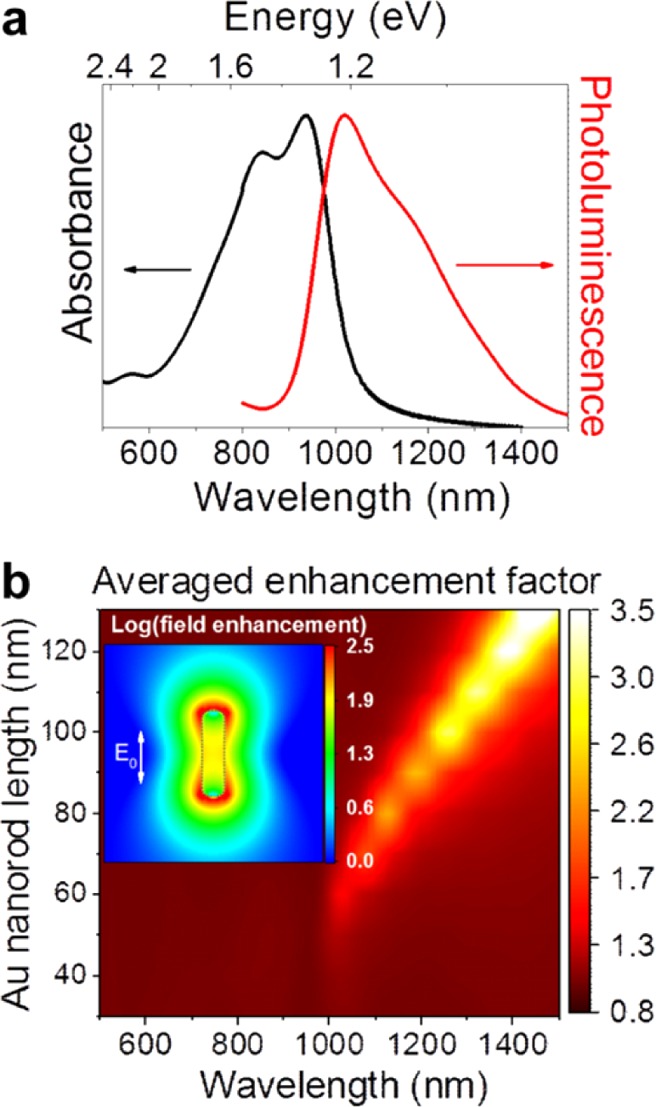
(a) Absorption and photoluminescence spectrum of a thin film of the semiconducting polymer DPPT-BT. (b) Simulated volume-averaged radiative decay rate enhancement as a function of the gold NR length (for a constant diameter of 20 nm), taking into account the random orientation of the NRs with respect to the emitting dipole. Inset: corresponding field enhancement distribution for 80 × 20 nm NRs.
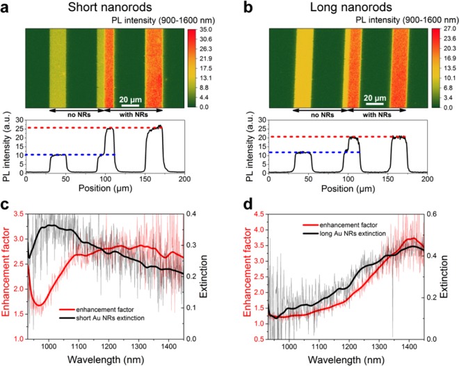
To investigate the coupling between photogenerated excitons (excited with a 785 nm laser) and LSPs we obtained PL intensity maps (integrated over the 900–1600 nm detection range, see Supporting Information) of the completed LEFETs. For better correlation of the experimental values with numerically calculated enhancement factors, we used two different sizes of NRs: short, with an average length of 70 nm, and long, with 130 nm in length. Both NR types were 20 nm in diameter (see Supporting Information, Figure S1, for extinction spectra). As can be seen from PL intensity maps and corresponding intensity profiles in Figure 3a,b, both NR types lead to an enhancement in emission that is not due to increased absorption (see above). The overall enhancement by the short nanorods is somewhat higher. A closer look at the wavelength-dependent enhancement factor defined as the ratio of PL intensity with to without NRs (averaged over 11 points) confirms this observation (Figure 3c,d). For short NRs, the enhancement factor of 2.75 is almost constant over the 1050–1400 nm spectral range, while for long NRs the enhancement factor increases up to 3.5 and peaks at 1400 nm. While the absolute enhancement value is higher for long NRs, its spectral position is in a region where only few photons are emitted by the DPPT-BT (Figure 2a). Thus, its overall contribution to the PL intensity is lower.
Figure 3.
(a, b) Photoluminescence intensity maps and corresponding profiles (bottom panels) of LEFET channels with short and long gold NRs, respectively, excited with a 785 nm laser. (c, d) Nanorod-induced, wavelength-dependent PL intensity enhancement factor for LEFET channels in (a, b) in comparison to extinction spectra of the corresponding gold NRs in the channel.
Comparing numerically calculated spectral changes with experimental data and extinction spectra of gold NRs measured directly on the devices, we gain additional insight into the coupling between LSPs and excitons in DPPT-BT. The spectral positions of the plasmon resonances correlate well with the theoretical values, that is, ∼1050 and ∼1400 nm for short and long NRs, respectively. Furthermore, while for long NRs the plasmon resonance also correlates with the maximum enhancement value, a minimum at around 960 nm is observed for short NRs in addition to the enhancement plateau. A similar dip is found in the numerically calculated enhancement factors. This is attributed to the spectral position where absorption and PL spectra overlap and thus plasmon-enhanced self-absorption is maximized (see Figure 2a,b). It is important to note that according to additional simulations the observed enhancement and spectral changes are not likely to be related to increased far-field scattering/outcoupling efficiency of the light trapped/guided within the polymer layer or any improved collection efficiency by the objective (see Supporting Information, Figures S6 and S7, for details).
Although numerical simulations of the enhancement factors can be used for a rough estimate of the expected values, its deviation from experimental values (especially for short NRs where enhancement over 1100–1400 nm is not expected) can be explained by the different NR densities and some degree of agglomeration leading to inter-NR coupling with the associated spectral changes. By comparing the experimental extinction spectra (Figure 3c,d) and theoretical extinction cross section spectra for single NRs (see Supporting Information, Figure S3) we found that the actual density of short (∼31.8 μm–2) and long NRs (∼13.8 μm–2) was somewhat higher than the one that was set in the simulations (∼11.1 μm–2).
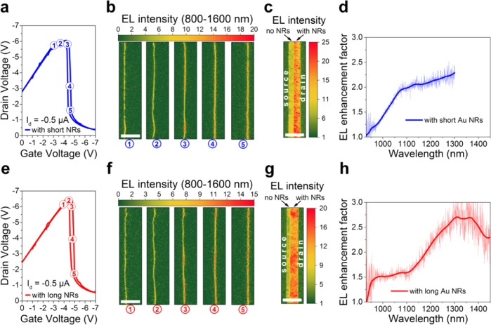
In order to switch from coupling between gold NRs and electrically generated excitons and no coupling, we performed gate voltage sweeps at a constant drain current for LEFETs with the channel half-covered with NRs as shown in Figure 1c. A constant drain current also means a fixed number of generated electron–hole pairs, that is, excitons, during the voltage sweep, independent from the position of the recombination zone. Hence, this sweep mode enables direct visualization of coupling to the NRs as manifested by an increased emission rate. Corresponding drain voltage versus gate voltage characteristics for LEFETs with short and long NRs are shown in Figure 4a,e. Transistors without any and fully covered with gold NRs (see Supporting Information, Figure S9) show the same change of drain voltage as the device enters the ambipolar regime. This is a typical observation for any type of ambipolar field-effect transistor.22 Although, the ambipolar output and transfer characteristics of LEFETs with and without NRs in the channel are not exactly identical (see Supporting Information, Figures S10–S12, for details) the overall impact of NRs on charge transport is very low and can be neglected for the constant current mode sweeps. Representative EL images (integrated over 800–1600 nm) for different gate voltages are shown in Figure 4b,f for short and long NRs, respectively. When the emission zone is positioned close to the region where NRs were deposited a significant increase of electroluminescence intensity is observed (see also video, Supporting Information). It is important to note that the width of the emission zone does not change during the sweep. The observable width of the emission zone in the EL images is about 1.5 μm and is limited by the emission wavelength, the collecting n-IR objective with a numerical aperture of 0.65 and the thickness of the glass substrate. The real width of the emission zone is likely to be much narrower and assuming Langevin-type recombination it should depend on the gate dielectric thickness,31 thus, making it suitable for the efficient coupling with subwavelength waveguiding components.
Figure 4.
(a, e) Gate voltage sweeps at constant drain current for LEFETs with short and long Au NRs, respectively. The applied voltages at which EL images in (b) and (f) were acquired are indicated (1–5). (b, f) Representative EL images show the movement of the emission zone and intensity increase due to coupling with Au NRs (4, 5 vs 1, 2). (c, g) Cumulative maximum EL intensity maps for LEFETs with short (c) and long (g) Au NRs. (d, h) Wavelength-dependent EL intensity enhancement factors for short (d) and long (h) Au NRs at drain current of 3 μA. The scale bar for (b, c, f, g) is 30 μm.
To further visualize the plasmonic coupling with the nanorods and the resulting EL enhancement the maximum intensity values for each pixel were extracted from the EL images during the constant current sweep as shown in Figure 4c,g. A clear difference between the areas with and without NRs is evident. In agreement with the PL enhancement (Figure 3a,b), the wavelength-integrated EL intensity increase is higher for short NRs compared to long NRs. Further comparison of the EL spectra acquired from the regions with and without NRs (see Supporting Information, Figure S13) and corresponding EL enhancement factors (see Figure 4d,h) correlate very well with the wavelength-dependent PL enhancement factors (Figure 3c,d) emphasizing its common origin, that is, the Purcell effect. Hence, efficient coupling between electrically excited excitons and LSPs is corroborated.
It is important to emphasize that the measured EL values are averaged over all positions of the emitting excitons in the emission zone with respect to the gold NRs. In other words, only a small share of emission from the DPPT-BT is actually enhanced by the Purcell effect. It is useful to calculate the local emission enhancement by taking into account an approximate area, in which most of the electromagnetic field is concentrated. Following the definition of effective mode area,32 we correct our enhancement factors for the confinement area (∼0.011 μm2) around the gold NRs and the experimental NR density (see Supporting Information for definition and calculation details). Thus, the local EL enhancement factors for short and long NRs become 12 (at 1100 nm) and 47 (at 1350 nm), respectively. It is necessary to mention that the actual region where enhancement occurs is slightly smaller (and local enhancement higher) due to the narrow zone around the gold NRs where NR-related quenching competes with radiative decay enhancement.33 The obtained values give an approximate magnitude of the actual local enhancement (although not measured directly) and entail the following important implications. First, plasmonic nanostructures are promising for an overall efficiency improvement of electroluminescent devices, especially if the light-emitting regions can be spatially confined. Second, the increased radiative decay and exciton–plasmon coupling rates boost the efficiency at which charge carriers are converted into plasmons and are thus not lost due to nonradiative relaxation.
In conclusion, we have demonstrated the fabrication and operation of light-emitting field-effect transistors as tunable electrical sources of surface plasmons. Precise voltage control over the position of the emission zone enables selective coupling to gold NRs resulting in electroluminescence enhancement depending on the size of NRs, which serves as a proof-of-principle for controlled exciton-LSP coupling in LEFETs. The charge transport properties of the LEFETs are almost unaffected by the gold NRs and thus more complex metallic nanostructures such as plasmonic waveguides should be feasible. We believe that these results will have a significant impact on the development of electrically driven, active plasmonic devices. LEFETs based on different semiconductors could be used to generate polychromatic plasmons from the visible to the infrared. Moreover, transistor channels can be designed to host multiple waveguiding components to which SPPs can be coupled selectively by simply changing the biasing conditions. The LEFET approach offers extended functionality compared to devices where the excitation of SPPs is spatially fixed (e.g., light-emitting diodes). Thus, LEFETs may serve as active components in future plasmonic circuits.
Acknowledgments
This research was financially supported by the European Research Council under the European Union’s Seventh Framework Programme (FP/2007-2013)/ERC Grant Agreement No. 306298 (EN-LUMINATE). J.Z. also thanks the Alfried Krupp von Bohlen und Halbach-Stiftung and the Cluster of Excellence “Engineering of Advanced Materials” (EXC 315) for general support.
Supporting Information Available
The Supporting Information is available free of charge on the ACS Publications website at DOI: 10.1021/acsphotonics.5b00413.
Methods: Synthesis and characterization of gold NRs, fabrication and characterization of LEFETs. Additional data and analysis: 3D-FDTD calculations, electrical characteristics of LEFETs with and without gold NRs, influence of gold NRs on EL spectra (PDF).
Near-infrared videos (wavelengths 800−1600 nm) of the recombination and emission zone from a LEFET channel half-covered with short gold NRs during a gate voltage sweep from −4.3 V to −2.6 V (AVI), and with long gold NR during a gate voltage sweep from −4.5 V to −3.9 V (AVI) each at a constant drain current (Id = −0.5 μA). One voltage step (2 mV) per frame and an integration time of 5 seconds were used.
The authors declare no competing financial interest.
Supplementary Material
References
- Ebbesen T. W.; Genet C.; Bozhevolnyi S. I. Surface-Plasmon Circuitry. Phys. Today 2008, 61, 44–50. 10.1063/1.2930735. [DOI] [Google Scholar]
- Koenderink A. F. Plasmon Nanoparticle Array Waveguides for Single Photon and Single Plasmon Sources. Nano Lett. 2009, 9, 4228–4233. 10.1021/nl902439n. [DOI] [PubMed] [Google Scholar]
- Grandidier J.; des Francs G. C.; Massenot S.; Bouhelier A.; Markey L.; Weeber J.-C.; Finot C.; Dereux A. Gain-Assisted Propagation in a Plasmonic Waveguide at Telecom Wavelength. Nano Lett. 2009, 9, 2935–2939. 10.1021/nl901314u. [DOI] [PubMed] [Google Scholar]
- De Leon I.; Berini P. Amplification of Long-Range Surface Plasmons by a Dipolar Gain Medium. Nat. Photonics 2010, 4, 382–387. 10.1038/nphoton.2010.37. [DOI] [Google Scholar]
- Gramotnev D. K.; Bozhevolnyi S. I. Plasmonics beyond the Diffraction Limit. Nat. Photonics 2010, 4, 83–91. 10.1038/nphoton.2009.282. [DOI] [Google Scholar]
- Cai W.; White J. S.; Brongersma M. L. Compact, High-Speed and Power-Efficient Electrooptic Plasmonic Modulators. Nano Lett. 2009, 9, 4403–4411. 10.1021/nl902701b. [DOI] [PubMed] [Google Scholar]
- Dionne J. A.; Diest K.; Sweatlock L. A.; Atwater H. A. PlasMOStor: A Metal–Oxide–Si Field Effect Plasmonic Modulator. Nano Lett. 2009, 9, 897–902. 10.1021/nl803868k. [DOI] [PubMed] [Google Scholar]
- Papaioannou S.; Kalavrouziotis D.; Vyrsokinos K.; Weeber J.-C.; Hassan K.; Markey L.; Dereux A.; Kumar A.; Bozhevolnyi S. I.; Baus M.; Tekin T.; Apostolopoulos D.; Avramopoulos H.; Pleros N. Active Plasmonics in WDM Traffic Switching Applications. Sci. Rep. 2012, 2, 1–9. 10.1038/srep00652. [DOI] [PMC free article] [PubMed] [Google Scholar]
- Melikyan A.; Alloatti L.; Muslija A.; Hillerkuss D.; Schindler P. C.; Li J.; Palmer R.; Korn D.; Muehlbrandt S.; Van Thourhout D.; Chen B.; Dinu R.; Sommer M.; Koos C.; Kohl M.; Freude W.; Leuthold J. High-Speed Plasmonic Phase Modulators. Nat. Photonics 2014, 8, 229–233. 10.1038/nphoton.2014.9. [DOI] [Google Scholar]
- Lee H. W.; Papadakis G.; Burgos S. P.; Chander K.; Kriesch A.; Pala R.; Peschel U.; Atwater H. A. Nanoscale Conducting Oxide PlasMOStor. Nano Lett. 2014, 14, 6463–6468. 10.1021/nl502998z. [DOI] [PubMed] [Google Scholar]
- Koller D. M.; Hohenau A.; Ditlbacher H.; Galler N.; Reil F.; Aussenegg F. R.; Leitner A.; List E. J. W.; Krenn J. R. Organic Plasmon-Emitting Diode. Nat. Photonics 2008, 2, 684–687. 10.1038/nphoton.2008.200. [DOI] [Google Scholar]
- Falk A. L.; Koppens F. H. L.; Yu C. L.; Kang K.; de Leon Snapp N.; Akimov A. V.; Jo M.-H.; Lukin M. D.; Park H. Near-Field Electrical Detection of Optical Plasmons and Single-Plasmon Sources. Nat. Phys. 2009, 5, 475–479. 10.1038/nphys1284. [DOI] [Google Scholar]
- Neutens P.; Van Dorpe P.; De Vlaminck I.; Lagae L.; Borghs G. Electrical Detection of Confined Gap Plasmons in Metal–insulator–metal Waveguides. Nat. Photonics 2009, 3, 283–286. 10.1038/nphoton.2009.47. [DOI] [Google Scholar]
- Walters R. J.; van Loon R. V. A.; Brunets I.; Schmitz J.; Polman A. A Silicon-Based Electrical Source of Surface Plasmon Polaritons. Nat. Mater. 2010, 9, 21–25. 10.1038/nmat2595. [DOI] [PubMed] [Google Scholar]
- Fan P.; Colombo C.; Huang K. C. Y.; Krogstrup P.; Nygård J.; Fontcuberta i Morral A.; Brongersma M. L. An Electrically-Driven GaAs Nanowire Surface Plasmon Source. Nano Lett. 2012, 12, 4943–4947. 10.1021/nl302521v. [DOI] [PubMed] [Google Scholar]
- Rai P.; Hartmann N.; Berthelot J.; Arocas J.; Colas des Francs G.; Hartschuh A.; Bouhelier A. Electrical Excitation of Surface Plasmons by an Individual Carbon Nanotube Transistor. Phys. Rev. Lett. 2013, 111, 026804. 10.1103/PhysRevLett.111.026804. [DOI] [PubMed] [Google Scholar]
- Cornil J.; Brédas J.-L.; Zaumseil J.; Sirringhaus H. Ambipolar Transport in Organic Conjugated Materials. Adv. Mater. 2007, 19, 1791–1799. 10.1002/adma.200602922. [DOI] [Google Scholar]
- Schornbaum J.; Zakharko Y.; Held M.; Thiemann S.; Gannott F.; Zaumseil J. Light-Emitting Quantum Dot Transistors: Emission at High Charge Carrier Densities. Nano Lett. 2015, 15, 1822–1828. 10.1021/nl504582d. [DOI] [PMC free article] [PubMed] [Google Scholar]
- Tersoff J.; Freitag M.; Tsang J. C.; Avouris P. Device Modeling of Long-Channel Nanotube Electro-Optical Emitter. Appl. Phys. Lett. 2005, 86, 263108. 10.1063/1.1957116. [DOI] [Google Scholar]
- Jakubka F.; Backes C.; Gannott F.; Mundloch U.; Hauke F.; Hirsch A.; Zaumseil J. Mapping Charge Transport by Electroluminescence in Chirality-Selected Carbon Nanotube Networks. ACS Nano 2013, 7, 7428–7435. 10.1021/nn403419d. [DOI] [PubMed] [Google Scholar]
- Zhang Y. J.; Oka T.; Suzuki R.; Ye J. T.; Iwasa Y. Electrically Switchable Chiral Light-Emitting Transistor. Science 2014, 344, 725–728. 10.1126/science.1251329. [DOI] [PubMed] [Google Scholar]
- Zaumseil J.; McNeill C. R.; Bird M.; Smith D. L.; Paul Ruden P.; Roberts M.; McKiernan M. J.; Friend R. H.; Sirringhaus H. Quantum Efficiency of Ambipolar Light-Emitting Polymer Field-Effect Transistors. J. Appl. Phys. 2008, 103, 064517. 10.1063/1.2894723. [DOI] [Google Scholar]
- Bisri S. Z.; Takenobu T.; Sawabe K.; Tsuda S.; Yomogida Y.; Yamao T.; Hotta S.; Adachi C.; Iwasa Y. P-I-N Homojunction in Organic Light-Emitting Transistors. Adv. Mater. 2011, 23, 2753–2758. 10.1002/adma.201004572. [DOI] [PubMed] [Google Scholar]
- Gwinner M. C.; Khodabakhsh S.; Song M. H.; Schweizer H.; Giessen H.; Sirringhaus H. Integration of a Rib Waveguide Distributed Feedback Structure into a Light-Emitting Polymer Field-Effect Transistor. Adv. Funct. Mater. 2009, 19, 1360–1370. 10.1002/adfm.200801897. [DOI] [Google Scholar]
- Baeg K.-J.; Noh Y.-Y.; Sirringhaus H.; Kim D.-Y. Controllable Shifts in Threshold Voltage of Top-Gate Polymer Field-Effect Transistors for Applications in Organic Nano Floating Gate Memory. Adv. Funct. Mater. 2010, 20, 224–230. 10.1002/adfm.200901677. [DOI] [Google Scholar]
- Davis A. R.; Pye L. N.; Katz N.; Hudgings J. A.; Carter K. R. Spatially Mapping Charge Carrier Density and Defects in Organic Electronics Using Modulation-Amplified Reflectance Spectroscopy. Adv. Mater. 2014, 26, 4539–4545. 10.1002/adma.201400859. [DOI] [PubMed] [Google Scholar]
- Ye X.; Zheng C.; Chen J.; Gao Y.; Murray C. B. Using Binary Surfactant Mixtures To Simultaneously Improve the Dimensional Tunability and Monodispersity in the Seeded Growth of Gold Nanorods. Nano Lett. 2013, 13, 765–771. 10.1021/nl304478h. [DOI] [PubMed] [Google Scholar]
- Thierry B.; Ng J.; Krieg T.; Griesser H. J. A Robust Procedure for the Functionalization of Gold Nanorods and Noble Metal Nanoparticles. Chem. Commun. 2009, 1, 1724–1726. 10.1039/b820137d. [DOI] [PubMed] [Google Scholar]
- Held M.; Schießl S. P.; Miehler D.; Gannott F.; Zaumseil J. Polymer/Metal Oxide Hybrid Dielectrics for Low Voltage Field-Effect Transistors with Solution-Processed, High-Mobility Semiconductors. Appl. Phys. Lett. 2015, 107, 083301. 10.1063/1.4929461. [DOI] [Google Scholar]
- Biteen J. S.; Sweatlock L. A.; Mertens H.; Lewis N. S.; Polman A.; Atwater H. A. Plasmon-Enhanced Photoluminescence of Silicon Quantum Dots: Simulation and Experiment. J. Phys. Chem. C 2007, 111, 13372–13377. 10.1021/jp074160+. [DOI] [Google Scholar]
- Kemerink M.; Charrier D. S. H.; Smits E. C. P.; Mathijssen S. G. J.; de Leeuw D. M.; Janssen R. A. J. On the Width of the Recombination Zone in Ambipolar Organic Field Effect Transistors. Appl. Phys. Lett. 2008, 93, 033312. 10.1063/1.2963488. [DOI] [Google Scholar]
- Oulton R. F.; Bartal G.; Pile D. F. P.; Zhang X. Confinement and Propagation Characteristics of Subwavelength Plasmonic Modes. New J. Phys. 2008, 10, 105018. 10.1088/1367-2630/10/10/105018. [DOI] [Google Scholar]
- Mertens H.; Koenderink A. F.; Polman A. Plasmon-Enhanced Luminescence near Noble-Metal Nanospheres: Comparison of Exact Theory and an Improved Gersten and Nitzan Model. Phys. Rev. B: Condens. Matter Mater. Phys. 2007, 76, 115123. 10.1103/PhysRevB.76.115123. [DOI] [Google Scholar]
Associated Data
This section collects any data citations, data availability statements, or supplementary materials included in this article.


