Abstract
Semiconductor heterostructures are fundamental building blocks for many important device applications. The emergence of two-dimensional semiconductors opens up a new realm for creating heterostructures. As the bandgaps of transition metal dichalcogenides thin films have sensitive layer dependence, it is natural to create lateral heterojunctions (HJs) using the same materials with different thicknesses. Here we show the real space image of electronic structures across the bilayer–monolayer interface in MoSe2 and WSe2, using scanning tunnelling microscopy and spectroscopy. Most bilayer–monolayer HJs are found to have a zig-zag-orientated interface, and the band alignment of such atomically sharp HJs is of type-I with a well-defined interface mode that acts as a narrower-gap quantum wire. The ability to utilize such commonly existing thickness terraces as lateral HJs is a crucial addition to the tool set for device applications based on atomically thin transition metal dichalcogenides, with the advantage of easy and flexible implementation.
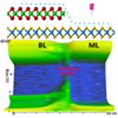 Heterojunctions of two-dimensional materials are used to design electronic and optoelectronic devices. Here, the authors show that zigzag terraces between monolayers and bilayers form atomically sharp type-I heterojunctions, resulting in a wire-like interface both in WSe2 and in MoSe2.
A heterojunction (HJ) is an interface between two different semiconductors. The difference in the electronic structures of the two materials results in potential discontinuities at the interface for electrons (conduction band offset) and holes (valence band offset). The introduction of heterostructures1 has enabled new types of electronic and photonic devices, transforming semiconductor technology. The recent emergence of two-dimensional (2D) semiconductors creates exciting new opportunities to push semiconductor heterostructures towards a new frontier2,3,4,5,6,7.
Vertically stacked van der Waals heterostructures have been quickly recognized as a powerful platform to create atomically thin heterostructures with great design flexibility2,8,9,10. Indeed, van der Waals heterostructures have been realized using different combinations of 2D materials, including transition metal dichalcogenides (TMDs), graphene and boron nitride11,12,13,14,15. Interesting properties, such as the observation of interface excitons16 and the determination of band alignments have been demonstrated recently in TMDs vertical heterostructures17. Less attention has gone to the possibility of creating ‘lateral HJs', where the junction is now a line interface between two 2D materials, reducing the dimensionality of heterostructures even further. Using direct chemical vapour deposition (CVD) growth, lateral junctions between different TMDs have been recently demonstrated18,19,20,21,22. However, theoretical calculations suggest that the heterostructures formed between the four most common TMD compounds (M=Mo, W; X=S, Se) all have type-II band alignment23,24, and the equally (if not more) important type-I HJs are still missing. How to create a lateral type-I HJ with an atomically sharp and straight interface, and characterize its band profile at the atomic scale, remain as significant challenges to overcome in order to advance this new frontier based on 2D semiconductors.
Previous investigations have shown that the bandgaps of TMD films greatly depend on the number of layers25,26. So one may naturally ask: can we create a well-defined lateral HJ between regions of different thicknesses, for example, a bilayer–monolayer interface? If so, is such a HJ type-I or type-II? Moreover, as the junction interface is also a step edge, how does this step edge influence the electronic structures of the HJ?
Here we study this new type of lateral heterostructures between bilayer (BL) and monolayer (ML) TMDs using low-temperature scanning tunnelling microcopy and spectroscopy (STM/S). We first show that atomically sharp and smooth interfaces with the desired type-I band alignment can indeed be formed. Moreover, we discover the presence of interface states with a narrow gap that act as interface quantum wires. Because the junction is formed between the direct gap monolayer TMD and the indirect gap bilayer TMD, the band edge carriers on the two sides of the junction are from different momentum space regions. This feature, coupled with the ability to control the interface through the edge states, offers the opportunity for novel device concepts in reduced dimensions.
Results
WSe2 bilayer–monolayer HJs
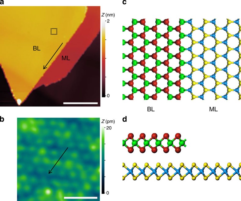
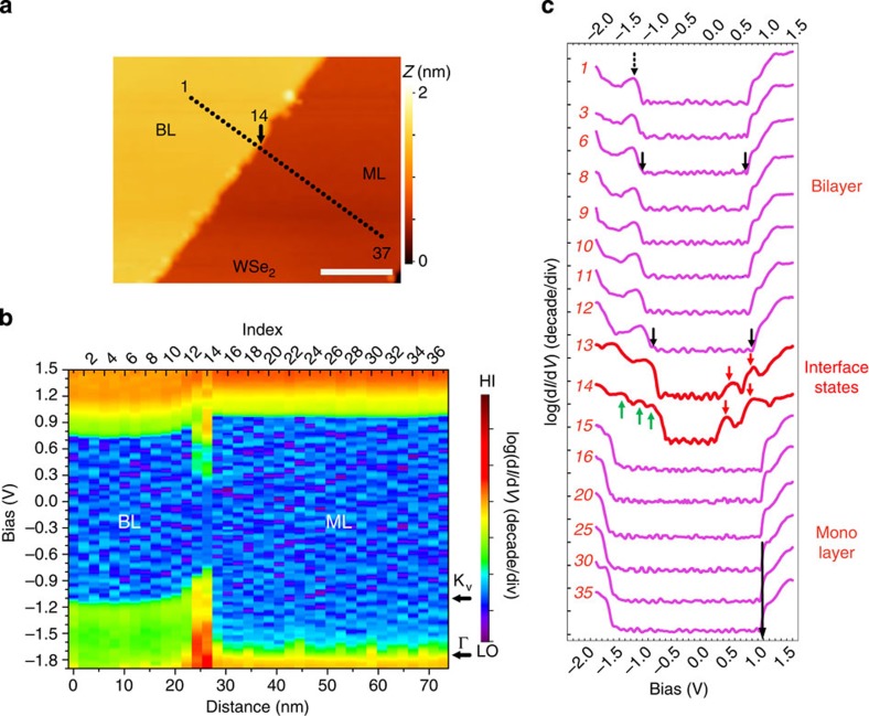
The BL–ML lateral HJs are formed naturally when a second layer of TMD is grown on top of the ML TMD. We achieve direct growth of such a HJ either using CVD27 or molecular beam epitaxy (MBE)26,28. Shown in Fig. 1a is an example of a WSe2 BL–ML heterostructure grown on a highly oriented pyrolytic graphite (HOPG) substrate using CVD. In this STM image, three distinct regions—graphite, ML–WSe2 and BL–WSe2—are separated by two atomically sharp line interfaces, corresponding to the ML and BL step edges (respectively separating graphite from ML WSe2, and ML from BL WSe2). An atomically resolved STM image (Fig. 1b) taken on the BL region allows us to determine the orientation of these two interfaces to be along the zig-zag directions. Then scanning tunnelling spectra are acquired to reveal the real space band profile across the interface. Figure 2a is a close-up STM image showing the spatial locations where STS given in Fig. 2b,c is carried out. Shown in Fig. 2b is a colour rendering of the band mapping result, and selected individual spectra are shown in Fig. 2c. Note that dI/dV spectra are displayed on a logarithmic scale. The numbers on the spectra refer to their position in the complete set, in which spectra are acquired every 2 nm from the BL into the ML region, with spectrum #14 acquired at the interface (Fig. 2a).
Figure 1. STM images and schematic models of BL–ML TMD lateral heterojunctions.
(a) STM image for a naturally formed BL–ML WSe2 HJ grown on HOPG by chemical vapour deposition. The bilayer and monolayer regions are labelled as shown. (b) Atomic resolution image taken on bilayer region where a dash square is labelled in a (not to scale). The sample biases and tunnelling currents used are (a) 3 V, 8 pA, (b) −1.0 V, 10 pA. The arrows in a and b indicate the zig-zag orientation of the bilayer–monolayer interface. (c,d) Schematic models of the BL–ML heterojunction viewing from top and side, respectively. The green and cyan represent the metal atoms in second and first layer respectively, while the red and yellow corresponding for chalcogen atoms. Scale bar, 100 nm (a); 1 nm (b).
Figure 2. Scanning tunnelling spectroscopy investigation of band profile across the BL–ML WSe2 heterojunction.
dI/dV spectra were taken along the path shown in (a). The spectra numbers are labelled (counting from left to the right in the path line). The total length is roughly 73 nm with a step size of 2 nm. Spectrum #14 was taken right at the interface. (b) Colour-coded rendering of the real space imaging of band profile plotted in terms of log(dI/dV). All spectra in this paper are displayed with arbitrary units (a.u.), except for Fig. 4c. The energy locations of Γ and KV (actual VBM) points are labelled by black arrows. (c) A selective subset of log(dI/dV) spectra. In spectrum #1, the upper state of Γ splitting, which results from interlayer coupling, is labelled with a black dashed arrow. The interface states are marked in spectrum #13 and #14 with red arrows for conduction band side and green arrows for valence band side. A black arrow in monolayer region represents for the energy location of CBM. Scale bar, 20 nm (a).
The most striking feature in Fig. 2b is the apparent band bending for both conduction band and valence band in the BL WSe2 near the interface. The magnitude of the band bending Δbend is about 0.15 eV over about 10 nm towards the interface (depletion length). One can also see an abrupt change in the electronic structure right at the BL–ML interface (see also spectrum #13 and #14 in Fig. 2c). The spectra in the ML region, in contrast, exhibit little band bending.
In the BL region, the dI/dV spectrum shows a prominent peak in the valence band (labelled with black arrow in spectrum #1 of Fig. 2c). This corresponds to the higher energy branch at the Γ point split due to the interlayer coupling. This feature has been discussed in detail recently29. The lower state is not visible in the limited energy window here. Far away from the interface, the valence band maximum (VBM) of BL region is located at −1.10±0.07 eV while the conduction band minimum (CBM) is determined to be 0.71±0.07 eV (from spectrum #1–#6), corresponding to a quasiparticle bandgap of 1.81±0.10 eV. From #6 to #12, the spectral line shape remains the same but the locations of the VBM and CBM both move upward, corresponding to the band bending (as indicated by the arrows in #6 and #12).
Right at the BL–ML interface, new spectral features emerge (#13 and #14 in Fig. 2c). Two prominent peaks around 0.4 and 0.8 eV (marked by the red arrows) appear in the conduction band. The new spectral features in the valence band can be observed more vividly on spectrum #14 (marked by the green arrows) but merge with the bulk valence states in #13. Interestingly, as revealed by the STS, the interface states here behave effectively like a narrow-gap semiconductor with a gap value of 0.8 eV (with VBM and CBM located roughly at −0.6 to 0.2 eV, respectively). Our STS map (Fig. 2b) suggests that the interface states have type-I band alignment with 2D bulk states of both the BL and ML therefore can play the role of a quantum wire for both electrons and holes. Localized interface states are actually a common feature of semiconductor interfaces having broken bonds, such as surfaces states at crystal-vacuum interfaces. In our case, broken bonds occur at the termination of the upper layer of bilayer TMD. Thus we may expect the quantum wire states to be centred on the atoms terminating the edge. However, the details of the step structure are not yet fully known.
Moving into the ML WSe2 region, one quickly observes the bulk ML WSe2 electronic structure without visible band bending within the spatial resolution (2 nm) of the STS. As one can see from spectrum #15 to #30 the electronic structure remains constant. It is important to recognize that in the ML WSe2 region, it is difficult to directly observe the actual VBM location (at K point in Brillouin zone) using conventional constant Z tunnelling spectroscopy as in Fig. 2b,c, due to the extremely short tunnelling decay length of K-points states29. The peak in the valence band corresponds to the energy location of the Γ point while the VBM at K point (not visible in the constant Z spectroscopy) is approximately located at 0.65 eV above. This point will be discussed further below.
As in any HJ, the energy alignment of the band edges (including the interface quantum wire) right at the interface is an inherent property, while the band bending depends on the electrostatics (for example the substrate). In the bulk ML and BL regions, the intimate contact with the graphite determines the location of EF in the gap. Near the edge, band bending occurs in order to keep the EF in the bandgap of the zig-zag quantum wire. The screening by the substrate graphite sets the length scale of the band bending at about 10 nm.
MoSe2 bilayer–monolayer HJs
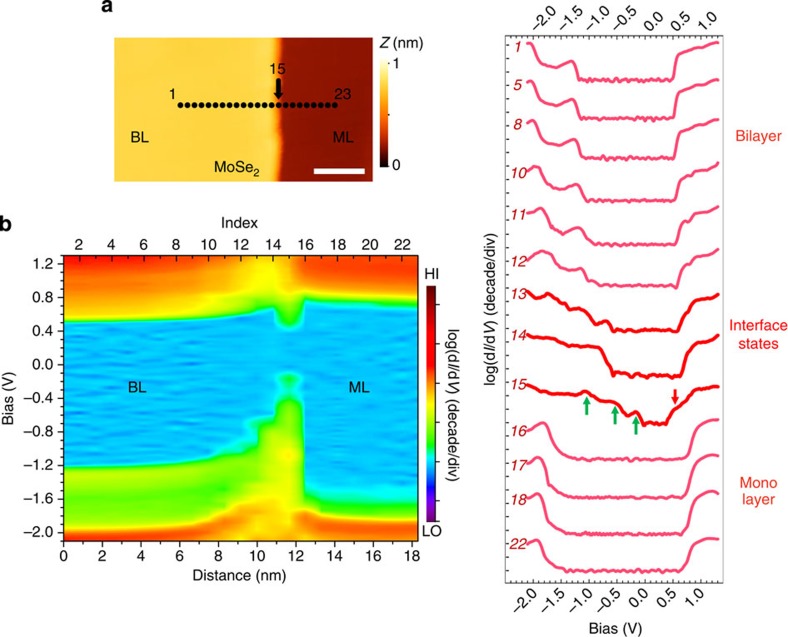
We have also studied the BL–ML heterostructure in MBE-grown MoSe2 on HOPG, where we find the same general behaviour as for WSe2, as illustrated in Fig. 3. The spatially resolved STS is acquired with a finer step of 0.8 nm (labelled in Fig. 3a). The colour rendering of band mapping based on the STS is shown in Fig. 3b. The upward band bending is observed for both conduction and valence bands. However, the ‘apparent' band bending from the valence band side is much stronger, effectively reducing the bandgap starting about 3–4 nm away from the edge. On detailed inspection, this is due to the overlap of valence band states of the bulk with those of the interface quantum wire states in the STS signal. One can see this more clearly from the individual STS spectra shown in Fig. 3c. Spectrum #10 still resembles the bulk BL band structure. On the other hand, in spectrum #11 the interface states above the bulk valence band edge start emerging and eventually split off (labelled by the green arrows in spectrum #15). This behaviour is similar to that in WSe2 discussed above except here the magnitude of the energy split off from the VBM of the bilayer is larger. The conduction band interface state is only observed right at the interface (#15, labelled by the red arrow). This might be due to a smaller energy split off from the CBM of the bilayer making it only observable very near the edge. The edge here has a narrower gap of 0.4 eV, which is also smaller than the one in WSe2. Moreover, with finer spatial resolution, we can observe a small band bending in ML region with a very short depletion length (around 1 nm only).
Figure 3. Scanning tunnelling spectroscopy investigation of band profile across the BL–ML MoSe2 heterojunction.
Similar with Fig. 2, (a) is a close-up STM image showing the path line that spectroscopy was taken along. The total length is about 18 nm with a step size of 0.8 nm. The spectra numbers in b and c are counted from left to right in the path, while spectrum #15 was taken right at the BL–ML interface. (b) Colour-coded rendering of the real space imaging of band profile plotted in terms of log(dI/dV). (c) Selective subset of log(dI/dV) spectra. In spectrum #15, the interface states in valence band and conduction band are marked with green and red arrows, respectively. Scale bar, 5 nm (a).
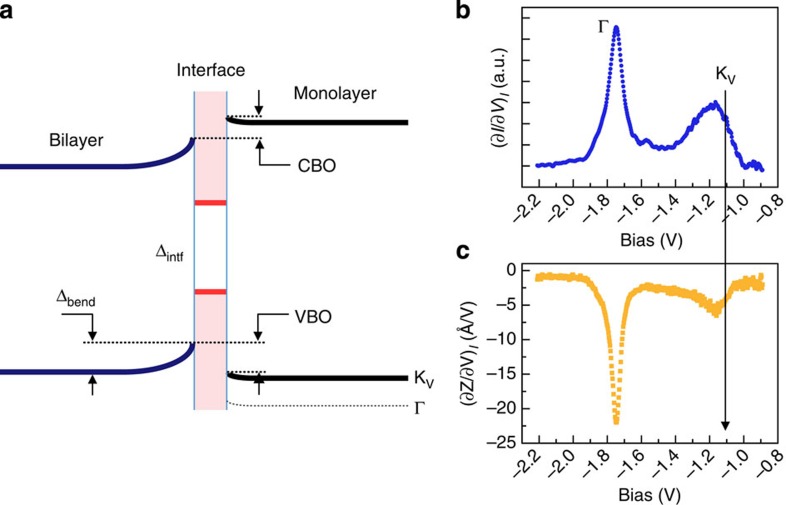
We summarize the general behaviour of lateral HJs formed from BL and ML WSe2 or MoSe2 with the schematic diagram (Fig. 4a) and Table 1. Here, the amount of the energy band bending is labelled as Δbend, the gap of the interface mode as Δintf, the valence band offset as VBO and the conduction band offset as CBO. The numerical values for these quantities are shown in Table 1 for WSe2 and MoSe2, respectively. As mentioned above, in the ML region, constant height tunnelling spectroscopy lacks the sensitivity to reveal the location of the VBM at the K point. On the other hand, as we reported recently29, constant-current spectroscopy can overcome this difficulty and resolve the states at the K point in the valence band (labelled as KV). As discussed extensively in ref. 29, in such constant-current spectroscopy, the individual thresholds at different critical points appear as peaks in differential conductivity (∂I/∂V)I as well as dips in the derivative of the tip-to-sample position as a function of the voltage (∂Z/∂V)I. Shown in Fig. 4b and c is the case for WSe2. The actual VBM is located at the mid-point of the transition from the TMD to the graphite states, which is around 0.65 eV above the Γ point, as labelled in Fig. 2b. For MoSe2, this value is 0.40±0.04 eV. With this information, we are able to determine that the CBO and VBO of BL–ML WSe2 HJs are 0.15±0.10 and 0.12±0.10 eV, respectively, as shown in Table 1. Similarly, for BL–ML MoSe2, they are found to be 0.08±0.10 and 0.43±0.10 eV, respectively, albeit in this case, the determined CBO is smaller than the experimental uncertainty of 0.1 eV.
Figure 4. Schematic diagram of band alignments and constant Z spectroscopy for valence band of ML WSe2.
(a) Schematic diagram showing the generic band alignment in BL–ML TMDs HJs. The magnitude of the band bending is labelled as Δbend, and the gap of interface states is Δintf. (b,c) Two modes of constant Z spectroscopy—(∂I/∂V)I and (∂Z/∂V)I for valence band of monolayer WSe2. The actual valence band maximum at K point is labelled as KV, which is about 0.65 eV above Γ point. See ref. 29 for details.
Table 1. Band alignments in bilayer-monolayer heterojunctions for WSe2 and MoSe2.
| BL–ML | Δbend (BL) | CBO | VBO | Δintf |
|---|---|---|---|---|
| WSe2 | 0.15±0.05 eV | 0.15±0.10 eV | 0.12±0.10 eV | 0.8±0.10 eV |
| MoSe2 | 0.08±0.10 eV | 0.43±0.10 eV | 0.4±0.10 eV |
BL, bilayer; CBO, conduction band offset; ML, monolayer; VBO, valence band offset.
The s.d.'s shown here are based on statistics of multiple measurements (more than 50 times).
Discussion
We first discuss the implications for electron transport across or along the interface which raises many interesting issues. It is well known for semiconductor HJs that there can be strong reflection at the interface, depending on how dissimilar the two material are. The same is true for reduced-dimensionality interfaces, such as HJs between ML and BL graphene30,31. Considering the significant differences of their electronic structures (especially band edges located at different k points in Brillouin zone), we may expect similar strong reflection at the interfaces of these BL–ML TMDs HJs. Transport along the interface can also be subject to scattering by imperfections. For example, the edge of the upper layer is in general not perfectly straight, so transport along the quantum wire will experience some disruption at kinks and other imperfections in the edge structure. This could lead to hopping conductivity with poor mobility along the wire. However, the non-ideal transport need not be an obstacle to important applications. In many conventional applications, the primary role of the HJ is to provide confinement, or to control barriers; and transport along or across the interface is secondary or even irrelevant. More important is that these interfaces provide a rich combination of barriers and localized states, offering novel opportunities for device engineering. Moreover we anticipate that the localized quantum wire states could be easily doped, since atoms tend to diffuse and bind at step edges.
In conclusion, our STM/STS studies reveal a new class of lateral HJ in atomically thin WSe2 and MoSe2, formed from naturally existing BL–ML thickness terraces with zig-zag orientation. Because of the thickness dependence of the bandgap and band edges, the ML and BL bulk bands align to form a type-I HJ, as clearly seen in our STS maps. The interface states in both systems form a narrow-gap quantum wire. This interface quantum wire has a gap value of 0.8 eV in WSe2 and a smaller gap value of 0.4 eV in MoSe2. The band alignment of the quantum wire states is also type-I with respect to both the BL and ML sides of the junctions. We expect that the unique properties of this novel class of HJs will create new possibilities for device applications based on 2D TMDs.
Methods
Growth of 2D TMDs samples
The preparation of WSe2 crystal flakes by the vapour-phase reaction has been reported before27. In brief, high purity metal trioxides WO3 was placed in a ceramic boat in the centre of a furnace, while graphite substrate was placed in the downstream side of the furnace, adjacent to the ceramic boat. Selenium powder was heated by a heating tape and carried by Ar or Ar/H2 gas to the furnace heating centre. The temperature of furnace was gradually raised from room temperature to the desired temperature, and cooled down naturally after the reaction had occurred. MoSe2 was grown on freshly cleaved HOPG substrate using MBE in an ultra-high vacuum (UHV) chamber which has a base pressure of 5 × 10⁻¹¹ torr. High-purity Mo (99.95%) and Se (99.999%) were evaporated from a home-built e-beam evaporator and an effusion cell, respectively, with a ratio of 1:30. The graphite substrate was kept at 550 °C, and the growth rate was about 0.3 layer per hour. The sample was annealed in a Se flux at 600 °C for 30 min after growth. Before STM studies, the CVD samples are cleaned in the UHV chamber (base pressure is <6 × 10⁻¹¹ torr) by annealing the sample at 300 °C for 6 h. The MBE samples are transferred in situ between the growth chamber and the STM chamber under UHV environment.
Scanning tunnelling microscopy and spectroscopy
All STM investigations reported here were acquired at 77 K in UHV (base pressure is <6 × 10⁻¹¹ torr). Electrochemically etched tungsten tips were cleaned in situ with electron beam bombardment. The tunnelling bias is applied to the sample. The conductance spectra were taken by using a lock-in amplifier with a modulation voltage of 10 mV and at a frequency of 924 Hz.
Additional information
How to cite this article: Zhang, C. et al. Visualizing band offsets and edge states in bilayer-monolayer transition metal dichalcogenides lateral heterojunction. Nat. Commun. 7:10349 doi: 10.1038/ncomms10349 (2016).
Acknowledgments
This research was supported with grants from the Welch Foundation (F-1672), and the US National Science Foundation (DMR-1306878, EFMA-1542747). W.Y. thanks the support from RGC of HKSAR (HKU9/CRF/13G) and HKU R.O.P. L.J.L. thanks the support from KAUST (Saudi Arabia), MOST and TCECM, Academia Sinica (Taiwan) and AOARD-134137 (USA). C.K.S is partially supported by the NT 3.0 Program, Ministry of Education.
Author contributions C.K.S., C.D.Z. and J.T. conceived the project. C.D.Z. carried out the STM/S measurement. Y.X.C. carried out MBE growth of MoSe2, J.K.H. and L.J.L. grew WSe2 by CVD. X.X.W. provided computational support for understanding the edge states. C.D.Z., C.K.S., W.Y. and J.T. analysed the data, interpret the data and wrote the paper.
01/21/2016
The HTML version of this Article previously published had an incorrect volume number of 6; it should have been 7. This has now been corrected in the HTML; the PDF version of the paper was correct from the time of publication.
References
- Kroemer H. in Nobel Lectures in Physics 1996–2000 ed. Ekspong G. 449 (World Scientific Publishing Co. Ptc. Ltd (2000). [Google Scholar]
- Geim A. K. & Grigorieva I. V. van der Waals heterostructures. Nature 499, 419–425 (2013). [DOI] [PubMed] [Google Scholar]
- Zeng Q. S. et al. Band engineering for novel two-dimensional atomic layers. Small 11, 1868–1884 (2015). [DOI] [PubMed] [Google Scholar]
- Gupta A., Sakthivel T. & Seal S. Recent development in 2D materials beyond graphene. Prog. Mater. Sci. 73, 44–126 (2015). [Google Scholar]
- Liu G.-B., Xiao D., Yao Y., Xu X. & Yao W. Electronic structures and theoretical modelling of two-dimensional group-VIB transition metal dichalcogenides. Chem. Soc. Rev. 44, 2643–2663 (2015). [DOI] [PubMed] [Google Scholar]
- Wang Q. H., Kalantar-Zadeh K., Kis A., Coleman J. N. & Strano M. S. Electronics and optoelectronics of two-dimensional transition metal dichalcogenides. Nat. Nanotechnol. 7, 699–712 (2012). [DOI] [PubMed] [Google Scholar]
- Zhang X. et al. Phonon and Raman scattering of two-dimensional transition metal dichalcogenides from monolayer, multilayer to bulk material. Chem. Soc. Rev. 44, 2757–2785 (2015). [DOI] [PubMed] [Google Scholar]
- Hong X. et al. Ultrafast charge transfer in atomically thin MoS2/WS2 heterostructures. Nat. Nanotechnol. 9, 682–686 (2014). [DOI] [PubMed] [Google Scholar]
- Fang H. et al. Strong interlayer coupling in van der Waals heterostructures built from single-layer chalcogenides. Proc. Natl Acad. Sci. USA 111, 6198–6202 (2014). [DOI] [PMC free article] [PubMed] [Google Scholar]
- Tongay S. et al. Tuning interlayer coupling in large-area heterostructures with CVD-grown MoS2 and WS2 monolayers. Nano Lett. 14, 3185–3190 (2014). [DOI] [PubMed] [Google Scholar]
- Britnell L. et al. Strong light-matter interactions in heterostructures of atomically thin films. Science 340, 1311–1314 (2013). [DOI] [PubMed] [Google Scholar]
- Withers F. et al. Light-emitting diodes by band-structure engineering in van der Waals heterostructures. Nat. Mater. 14, 301–306 (2015). [DOI] [PubMed] [Google Scholar]
- Lee C. H. et al. Atomically thin p-n junctions with van der Waals heterointerfaces. Nat. Nanotechnol. 9, 676–681 (2014). [DOI] [PubMed] [Google Scholar]
- Furchi M. M., Pospischil A., Libisch F., Burgdorfer J. & Mueller T. Photovoltaic effect in an electrically tunable van der Waals heterojunction. Nano Lett. 14, 4785–4791 (2014). [DOI] [PMC free article] [PubMed] [Google Scholar]
- Cheng R. et al. Electroluminescence and photocurrent generation from atomically sharp WSe2/MoS2 heterojunction p-n diodes. Nano Lett. 14, 5590–5597 (2014). [DOI] [PMC free article] [PubMed] [Google Scholar]
- Rivera P. et al. Observation of long-lived interlayer excitons in monolayer MoSe2–WSe2 heterostructures. Nat. Commun. 6, 6242 (2015). [DOI] [PubMed] [Google Scholar]
- Chiu M.-H. et al. Determination of band alignment in the single-layer MoS2/WSe2 heterojunction. Nat. Commun. 6, 7666 (2015). [DOI] [PMC free article] [PubMed] [Google Scholar]
- Huang C. et al. Lateral heterojunctions within monolayer MoSe2–WSe2 semiconductors. Nat. Mater. 13, 1096–1101 (2014). [DOI] [PubMed] [Google Scholar]
- Gong Y. J. et al. Vertical and in-plane heterostructures from WS2/MoS2 monolayers. Nat. Mater. 13, 1135–1142 (2014). [DOI] [PubMed] [Google Scholar]
- Zhang X. Q., Lin C. H., Tseng Y. W., Huang K. H. & Lee Y. H. Synthesis of lateral heterostructures of semiconducting atomic layers. Nano Lett. 15, 410–415 (2015). [DOI] [PubMed] [Google Scholar]
- Duan X. et al. Lateral epitaxial growth of two-dimensional layered semiconductor heterojunctions. Nat. Nanotechnol. 9, 1024–1030 (2014). [DOI] [PubMed] [Google Scholar]
- Li M. Y. et al. Epitaxial growth of a monolayer WSe2-MoS2 lateral p-n junction with an atomically sharp interface. Science 349, 524–528 (2015). [DOI] [PubMed] [Google Scholar]
- Gong C. et al. Band alignment of two-dimensional transition metal dichalcogenides: application in tunnel field effect transistors. Appl. Phys. Lett. 103, 053513 (2013). [Google Scholar]
- Kang J., Tongay S., Zhou J., Li J. & Wu J. Band offsets and heterostructures of two-dimensional semiconductors. Appl. Phys. Lett. 102, 012111 (2013). [Google Scholar]
- Mak K. F., Lee C., Hone J., Shan J. & Heinz T. F. Atomically thin MoS2: a new direct-gap semiconductor. Phys. Rev. Lett. 105, 136805 (2010). [DOI] [PubMed] [Google Scholar]
- Zhang Y. et al. Direct observation of the transition from indirect to direct bandgap in atomically thin epitaxial MoSe2. Nat. Nanotechnol. 9, 111–115 (2014). [DOI] [PubMed] [Google Scholar]
- Huang J. K. et al. Large-area synthesis of highly crystalline WSe2 mono layers and device applications. ACS Nano 8, 923–930 (2014). [DOI] [PubMed] [Google Scholar]
- Liu H. et al. Dense network of one-dimensional midgap metallic modes in monolayer MoSe2 and their spatial undulations. Phys. Rev. Lett. 113, 066105 (2014). [DOI] [PubMed] [Google Scholar]
- Zhang C. et al. Probing critical point energies of transition metal dichalcogenides: surprising indirect gap of single layer WSe2. Nano Lett. 15, 6494–6500 (2014). [DOI] [PubMed] [Google Scholar]
- Giannazzo F., Deretzis I., La Magna A., Roccaforte F. & Yakimova R. Electronic transport at monolayer-bilayer junctions in epitaxial graphene on SiC. Phys. Rev. B 86, 235422 (2012). [Google Scholar]
- Ji S. H. et al. Atomic-scale transport in epitaxial graphene. Nat. Mater. 11, 114–119 (2012). [DOI] [PubMed] [Google Scholar]


