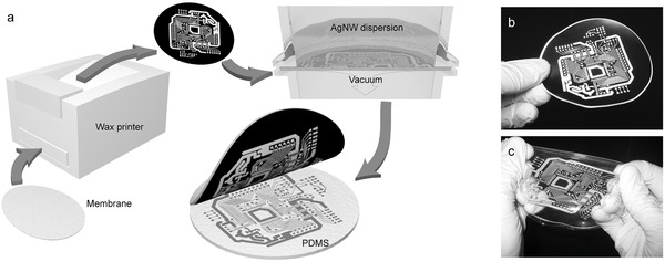
Figure 1.

Nanowire conductor patterning. a) The PVDF membrane is mounted on a paper carrier and the wax pattern is printed onto the membrane. The patterned membrane is mounted in a filtration setup and the AgNW dispersion is filtered through the uncovered areas of the membrane. The AgNW pattern is transferred to a semicured PDMS substrate under pressure and finally the membrane is peeled off. b) Example of a wax pattern printed onto a membrane of 90 mm in diameter. c) The AgNW pattern has been transferred onto a stretchable PDMS substrate.
