Abstract
In the field of iron-based superconductors, one of the frontier studies is about the pairing mechanism. The recently discovered (Li1−xFex)OHFeSe superconductor with the transition temperature of about 40 K provides a good platform to check the origin of double superconducting gaps and high transition temperature in the monolayer FeSe thin film. Here we report a scanning tunnelling spectroscopy study on the (Li1−xFex)OHFeSe single crystals. The tunnelling spectrum mimics that of the monolayer FeSe thin film and shows double gaps at about 14.3 and 8.6 meV. Further analysis based on the quasiparticle interference allows us to rule out the d-wave gap, and for the first time assign the larger (smaller) gap to the outer (inner) Fermi pockets (after folding) associating with the dxy (dxz/dyz) orbitals, respectively. The gap ratio amounts to 8.7, which demonstrates the strong coupling mechanism in the present superconducting system.
 Whilst superconductivity is understood to emerge when electronic
pairing allows for conduction without resistance, the mechanism at work in Fe-based
superconductors is unclear. Here, the authors address the details of Fermi surfaces and
associated gaps as well as the pairing mechanism of (Li1−x
Fe
x
)OHFeSe via scanning tunnelling methods.
The pairing mechanism and the superconducting gap structure have remained as the core
issues in the study on iron-based superconductors. Depending on the atomic structures,
the Fermi surface topology changes significantly in different systems, varying from
having hole pocket(s) only, to both hole and electron pockets, and to only electron
pockets in some FeSe-based systems1,2,3,4,5,6,7. In many earlier
discovered FeAs- or FeSe-based systems8,9,10 with both electron and
hole pockets, a natural pairing picture was proposed11,12, which
concerns the pairing through the pair-scattering process between the electron and hole
pockets leading to an extended s-wave gap with the pairing manner denoted by
s±. While in the system with absence of the hole
pockets, this weak coupling-based picture is facing a great challenge. The question
arising immediately is that whether we have a sign change of the gap function as
expected from the repulsive interaction-induced pairing13, for example,
the nodeless d-wave with opposite signs between two neighbouring electron
pockets. Another puzzling point is that in the scanning tunnelling
microscopy/spectroscopy (STM/STS) measurements on the FeSe monolayer thin film1 on a SrTiO3 substrate, double gaps have been observed on the
single tunnelling spectrum with the larger gap ranging from 14 to 22 meV,
while in all the angle-resolved photoemission spectroscopy (ARPES) measurements3,4 there is only one set of electron Fermi pockets near the  point. It is curious to know how to associate the double gaps
with only one set of Fermi pockets. In addition, the larger gap discovered either in
STM/STS1 or ARPES3,4 measurements is very big in a
sense of weak coupling-based picture. Therefore it was proposed that some interfacial
strong phonon mode may join in the electron-boson coupling leading to the high gap
value2. However, this scenario needs to be verified in systems
without the particular substrate and related phonons. It is thus highly desired to do
experiments in the FeSe-based system with the similar electronic structures. The
recently discovered (Li1−xFex)OHFeSe
phase5,6,7 with a superconducting transition temperature
Tc≈40 K shows also only electron pockets around
 points in a folded Brillouin zone (BZ)14,15, which is very similar to the case of monolayer FeSe thin film. This
provides us a very good platform to check the fundamental problems, such as the origin
of the double gaps and whether the weak coupling-based picture holds still for the
superconductivity mechanism.
In this paper, we report the STM/STS measurements on the newly discovered superconductor
(Li1−xFex)OHFeSe. It is found that
the tunnelling spectrum shows a double gap structure and looks very similar to that
observed on the FeSe monolayer thin film. The analysis based on the quasiparticle
interference (QPI) technique allows us to carefully scrutinize the superconducting gaps
on the associated Fermi surfaces near  points in
(Li1−xFex)OHFeSe. The larger gap
(Δ1) derived here is about 14.3 meV, which yields a
huge gap ratio of
2Δ1/kBTc=8.7. This
demonstrates the strong coupling mechanism for superconductivity in the present system.
Our work shed new light in understanding the puzzling issues in the high-temperature
superconducting FeSe monolayer thin films, and will stimulate new efforts in solving the
superconductivity mechanism in iron-based superconductors.
Results
Characterization of superconducting properties
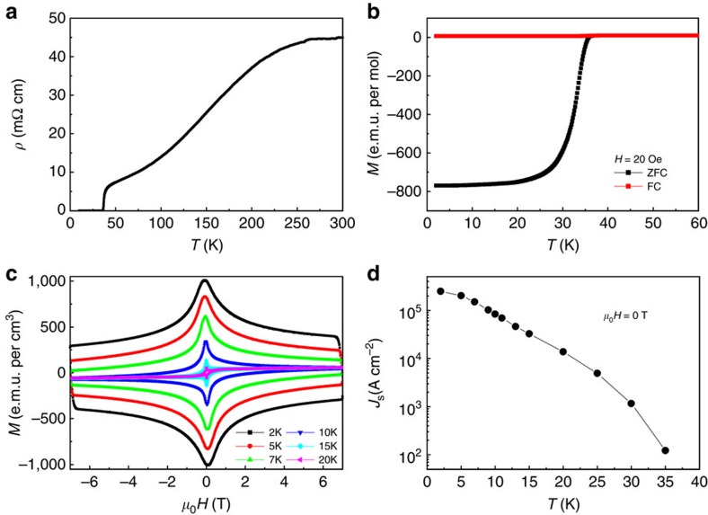
Figure 1a shows the temperature-dependent resistivity of the (Li1−xFex)OHFeSe single crystal. One can see that the resistive transition is rather sharp near the foot. The rounded shape near the onset transition is induced by the fluctuating superconductivity since the system is highly two-dimensional (2D). In Fig. 1b, we present the temperature dependence of the DC magnetization of the sample. It is measured at an external magnetic field of 20 Oe with the zero-field-cooled (ZFC) and FC modes. The sample shows perfect Meissner shielding effect with the superconducting transition temperature around 38 K, which is comparable to previous reports5,6,7. The magnetization-hysteresis-loops shown in Fig. 1c exhibit a symmetric feature, which suggests the bulk pinning of vortices and thus the bulk superconductivity of the material. The calculated critical current density at 2 K and 0 T from the Bean critical state model16 shown in Fig. 1d is 1–2 orders of magnitude larger than that in KxFe2−ySe2 and is comparable to that in the optimally doped Ba(Fe1−xCox)2As2 (ref. 17). This indicates that the sample is not phase separated as what occurs in KxFe2−ySe2. This allows us to have reliable STM/STS measurements.
Figure 1. Superconducting transition and magnetization of the (Li 1− x Fe x )OHFeSe crystal.
(a) Temperature dependence of resistivity of the sample. (b) Temperature dependence of DC magnetization measured with the zero-field-cooled (ZFC) and field-cooled (FC) modes at a field of 20 Oe. (c) The magnetization-hysteresis-loops measured at temperatures from 2 to 20 K. (d) Temperature dependence of the calculated critical current density Js based on the Bean critical state model at zero magnetic field.
Topographic STM image and STS spectra
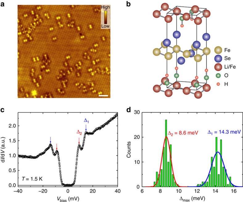
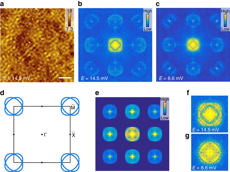
STM/STS measurements can provide essential information on the electronic structure and the gap symmetry of the novel superconductors18,19,20. Figure 2a shows a topographic image of the terminated surface of the cleaved (Li1−xFex)OHFeSe single crystal, and the atomically resolved square lattice is clearly seen. The lattice constants at the perpendicular directions are 3.61 and 3.63 Å, respectively, which are comparable to the lattice constant a of 3.79 Å from previous reports5,7. The schematic structure of (Li1−xFex)OHFeSe is shown in Fig. 2b. Since the cleaved surface is very stable and the lattice constant is very close to the expected value of Se–Se bond, together with the perfect STS measured (see below), we can reasonably assume that the terminated top layer is the Se-atom layer. Some bright spots with a dumbbell shape on the topography are observed and very similar to those from Cu or Co impurities in our previous works21,22. From the structure of the system, it is found that the impurity atom in the centre of a dumbbell spot locates just at the position of an Fe atom in the beneath layer, and it may be induced by the partial substitution of Fe atoms with Li, or some vacancies at the Fe sites in the Fe layer. This can get support from previous results on LiFeAs in which similar defects on Fe sites were proposed23,24,25. The calculated density of the impurities varies from 0.5 to 1.5% of Fe sites on the FeSe layer, which is much lower than the ratio of about 20% of substitution of Li by Fe atoms in the Li(Fe) layers5,6,7.
Figure 2. Topographic STM image and two-gap feature of (Li 1− x Fe x )OHFeSe.
(a) The atomically resolved STM image with a bias voltage of Vbias=180 mV and tunnelling current of It=102 pA. The defects with the dumbbell shape are observed on the top surface. Scale bar, 2 nm. (b) The schematic atomic structure of (Li1−xFex)OHFeSe. (c) A typical STS spectrum measured at 1.5 K away from the defects. One can clearly see the two-gap feature. Similar STS with double gap structure have been repeated in different areas and different samples. (d) Histogram of the superconducting gap values with the fitting results by Gaussian functions (solid lines). Two major gaps can be found.
Figure 2c shows a typical tunnelling spectrum measured at 1.5 K. Clearly there are two pairs of coherence peaks on the spectrum, indicating existence of two superconducting gaps. The larger gap is marked by Δ1 on its peak position of about ±14.3 meV while the smaller one is marked by Δ2 at about ±8.6 meV. The spectrum with two-gap feature is reminiscent of that reported on the monolayer FeSe thin film on SrTiO3 substrate1. The recent high-resolution ARPES measurements show only electron pockets as well as one superconducting gap in (Li1−xFex)OHFeSe14,15. It should be noted that the two-gap feature in the monolayer FeSe thin film was observed only in the STS measurements1, not in the ARPES. This may be induced by the limited resolution of ARPES, or due to some selection rules in the emission process of photo-electrons. More interestingly, the gaps found by the two ARPES measurements from two different groups on the similar samples are corresponding to the larger14 and smaller gap15 maxima of our STS measurements, respectively. The two-gap feature is a common one in our (Li1−xFex)OHFeSe samples, which can get support from the statistical result (Fig. 2d) of the peak positions on 98 spectra collected randomly in the range of 41 nm × 41 nm. By fitting to the Gaussian functions, we obtained the two-gap values of Δ1=14.3±1.3 and Δ2=8.6±0.9 meV, and the corresponding gap ratios of 2Δ1/kBTc=8.7±0.8 and 2Δ2/kBTc=5.2±0.5. These values are much larger than the one 2Δ/kBTc∼3.53 predicted by the Bardeen–Cooper–Schrieffer (BCS) theory in the weak coupling regime. The huge value 2Δ1/kBTc=8.7 indicates strong coupling mechanism in the system. Worthy of noting is that similar ratio was observed in the cuprate superconductors26,27.
Temperature-dependent STS spectra and Dynes model fitting
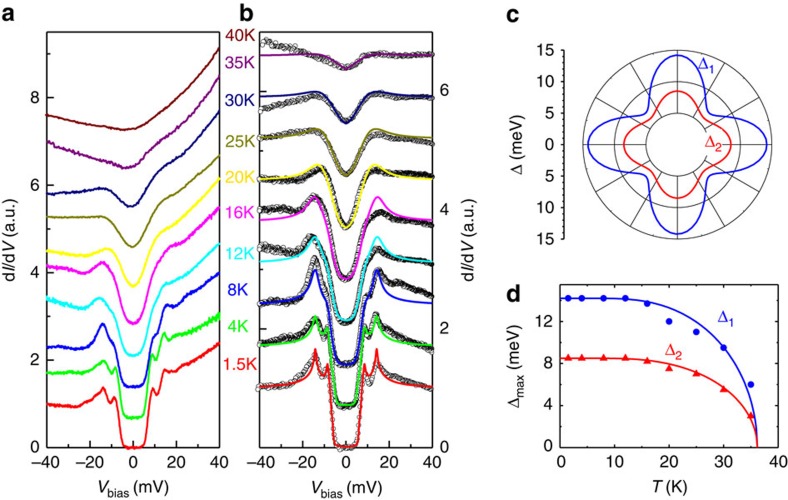
In Fig. 3a, we show the temperature evolution of the
tunnelling spectra measured at the same position. The coherence peaks
associating with both gaps are suppressed and mix together with increasing
temperature, and finally vanish above Tc. To see the possible
influence of the electronic bands on the tunnelling spectrum, we show one STS
measured in wide energy ranges in Supplementary Fig. 1. The spectra shown in Fig.
3b are normalized (divided by the one measured at 40 K).
The two well-resolved coherence peaks together with the fully gapped density of
states (DOS) near zero-bias allow us to make reliable fitting using the Dynes
model28. From the normalized spectrum at 1.5 K,
one can see that the bottom of the STS is very flat and has a zero value,
however, the coherence peaks are not very sharp. Together with the latter effect
is the finite slope of the rising edges of the STS near the bottom. To know
whether these contradicting phenomena are induced by the finite scattering
rates, we firstly try to use two isotropic s-wave gaps and different
pairs of scatterings rates Γ1(2) to fit the
experimental data. Because of the two-gap feature, in the model to fit the
normalized spectra, the differential conductivity is constructed as:
G=xdI1/dV+(1−x)dI2/dV,
where I1(2)(V) is the tunnelling current contributed by
the larger(smaller) gap, and x is the related spectral weight. The
detailed fitting process and parameters are given in Supplementary Note 1. The fitting results
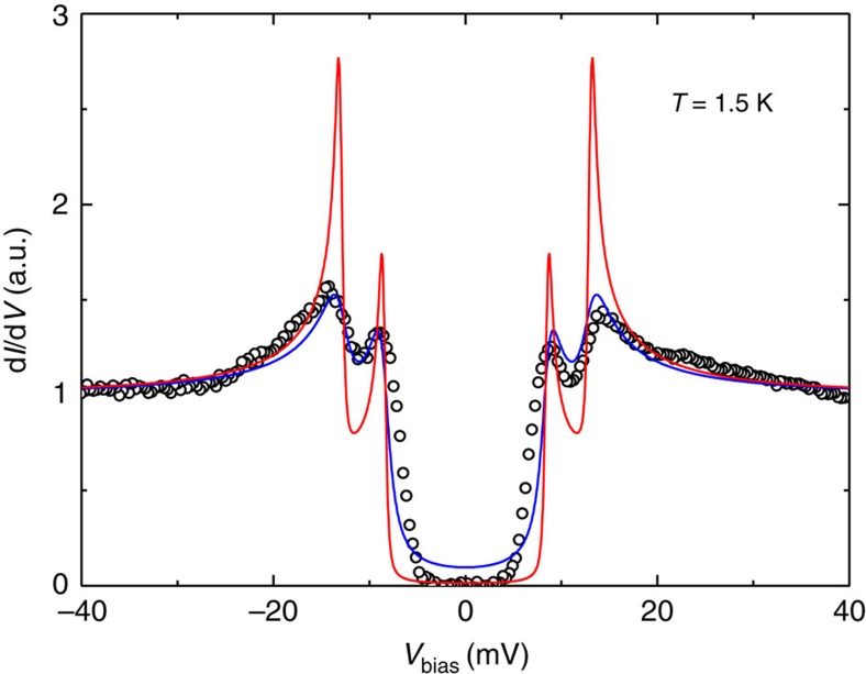
with two isotropic s-wave gaps under zero and finite scattering rates are
presented in Fig. 4. It is clear that, even with the
finite scattering rates, the fitting with isotropic gaps fails to catch up the
main features of the experimental data. We then use the two anisotropic
s-wave gaps  to fit the experimental data
and show the results in Fig. 3b. One can see from Fig. 3b that the theoretical model fits the experimental
data very well. The fitting process is detailed in Supplementary Note 1 and the fitting
parameters are listed in Supplementary
Table 1. The fourfold symmetric gap functions used to fit the data at
1.5 K are presented in Fig. 3c, and the
anisotropy p is fixed in all the fittings, that is, 25% for
Δ1(θ) and 15% for
Δ2(θ), while the weight of the larger
gap Δ1(θ) is fixed with the value of
65% at different temperatures. The resultant gap maxima versus
temperature are shown in Fig. 3d, and the solid lines are
the results of theoretical calculation within the BCS model by fixing
Δmax(0) and Tc derived from our
experiment. One can see that the temperature-dependent superconducting gaps can
be well-described by the BCS theory. Our results suggest that this material has
two nodeless superconducting gaps, each with a significant anisotropy. The
two-gap feature is difficult to be understood if only one set of electron Fermi
pockets around the
  point exists as observed in the
ARPES measurements.
Figure 3. Temperature-dependent tunnelling spectra and theoretical fits.
(a) The evolution of the STS spectra measured at temperatures from 1.5 to 40 K. (b) Fitting results to the STS spectra normalized by the one measured at 40 K in the normal state. The dark hollow circles represent the experimental data, and the coloured solid lines are the theoretical fits to the data with two anisotropic s-wave gaps by the Dynes model. (c) The anisotropic-gap functions used in the fitting to the curve measured at 1.5 K. (d) Temperature dependence of the two gaps extracted from the Dynes model fitting, and the solid lines denote the theoretical calculations of the superconducting gap from the BCS model.
Figure 4. Theoretical fitting results by two isotropic s -wave gaps.
The fitting results shown as solid lines with different fitting parameters fail to catch up the main features of the experimental data. For the fittings, Δ1=13 meV and Δ2=8.5 meV, Γ1=Γ2=0.15 meV were used for the clean case (red line), while the same gaps and Γ1=1.2 and Γ2=0.85 meV for the case of finite scattering rates (blue one). From these fittings, one can see that the tunnelling spectrum cannot be fitted with two isotropic gaps.
QPI measurements
On the surface of the crystal, we can see some dumbbell-shape impurities. The
spectrum measured on the impurity site has no well-defined superconducting
coherence peaks as shown in Supplementary Note 2. Instead, we can see the in-gap states with two
asymmetric peaks which make the bottom near zero-bias
‘V'-shaped (Supplementary Fig. 2). The impurities which act as the scattering
centres will produce the standing waves, and such QPI imaging can provide
fruitful information on the scattering between the contours of Fermi surfaces
with the scattering vector q at constant energy E in
k-space20. We perform the QPI measurements on two
areas with different scanning range as their topographies shown in Supplementary Fig. 3a,b. The details of the
measurements of QPI and data treatments are given in Supplementary Note 3. The standing waves can
be clearly seen in Fig. 5a measured around the larger
energy gap Δ1. When we do the Fourier transformation (FT)
to the QPI image, the resultant ρ(q, E) image, or
called as the FT-QPI image, shown in Fig. 5b,c helps us to
investigate the Fermi surfaces and the superconducting gaps of the material. The
resultant FT-QPI pattern looks quite similar to the data on the monolayer FeSe
thin film on SrTiO3 (001) as recently revealed by the STM
measurement29. Quite interestingly, the contours near the
corner of the FT-QPI pattern corresponding to the large-q scattering have
clear anisotropic feature, which was also observed on the monolayer FeSe thin
film on SrTiO3 (001) and was attributed to the orbital features29. The ARPES14,15 measurements show only one set
of electron pockets near  points. However, if
taking a closer look at the central part of the FT-QPI images as shown in Fig. 5f,g, we can find that it is unlikely. There are
actually two circles, which means that a single set of isotropic ring-shaped
Fermi surfaces would not be possible to produce such patterns. Therefore we use
elliptic electron Fermi surfaces to simulate the QPI image. Because there are
two Fe sites and two distinct Se sites in one unit cell, the two slightly
elliptic Fermi pockets will naturally fold into the smaller BZ, as sketched in
Fig. 5d. In the picture of folded Fermi surfaces, we
can consider the Fermi pockets as inner and outer rings. Due to the possible
spin-orbital coupling, the two Fermi pockets may further hybridize into two sets
of Fermi pockets with inner and outer contours30. We thus do the
QPI simulation of this type of Fermi pockets and the resultant pattern (Fig. 5e) is comparable with our experimental data. As shown
in Fig. 5b,c, when the bias voltage was increased from
Δ2max=8.6 to
Δ1max=14.5 meV, the peripheral
patterns from the inter-pocket scattering have negligible difference while the
pattern in the centre corresponding to the intra-pocket scattering changes a
lot. The magnitude of the outer circle in the central pattern (Fig. 5f,g) seems to be enhanced obviously when the energy increases
from the small energy gap to the larger one. The intensity of the FT-QPI contour
reflects the joint DOS (JDOS) between two k-points on the Fermi surfaces.
The emergence and enhancement of intensity in the contour in q-space of
the outer circle at a higher energy suggests that the superconducting gap on
this Fermi surface is larger than that of the inner one31,32,33.
Figure 5. Quasiparticle interference patterns and theoretical simulation.
(a) QPI image g(r, E=14.5 mV) in real space measured at 1.7 K near the energy of the coherence peak position of the larger gap. Scale bar, 5 nm. (b,c) FT-QPI intensity ρ(q, E) obtained by taking Fourier transformations on the corresponding real-space image measured with energies near the coherence peak position of the two gaps, namely 14.5 and 8.6 mV. The images are fourfold symmetrized to enhance the signal. (d) Schematic plot of the elliptic-shaped electron pockets in folded Brillouin zone. (e) The theoretical simulation of the QPI scattering intensity by applying autocorrelation to d. (f,g) Zoom-in images of the central parts of b and c, which contain the information of the small-q intra-pocket scattering. The image at 14.5 mV is very similar to the structure of the central pattern in (e). However the central pattern at 8.6 mV has a very different shape, and the outer ring seems to be less pronounced.
Intraband QPI
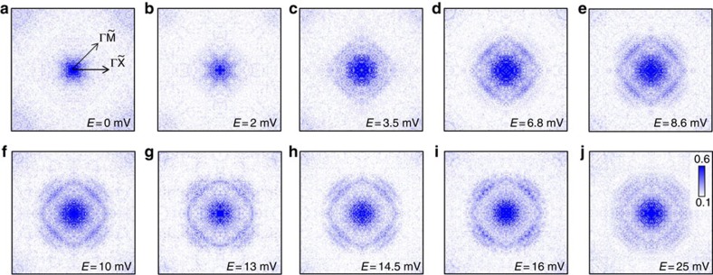
We then pay attention to the central pattern by measuring the QPI mapping in a
larger real-space scale to get the detailed features of the smaller
q-space view, and the evolution of the ρ(q,
E) images is shown in Fig. 6. The raw data of
the related QPI images are given in Supplementary Fig. 4. One can see that there is almost nothing at the
locations of the two interference rings at the energy of 0 and 2 mV.
This may rule out the existence of any gap nodes on the Fermi surface, since the
FT-QPI images would show an intensity at the q-vector connecting two
nodal points if they would exist. This is also consistent with the full gap
structure as seen from the STS spectrum. At the energy of 6.8 mV, a
ring with enhanced intensity on the FT-QPI images can be observed, with the
strongest intensity along the  direction. At the
energy of the small gap, namely 8.6 mV, the FT-QPI pattern looks
similar to that at 6.8 mV. However, when the energy is further
increased to the larger gap, that is, 14.5 mV, besides the inner
ring, a new set of segments appears at larger q vectors, which gradually
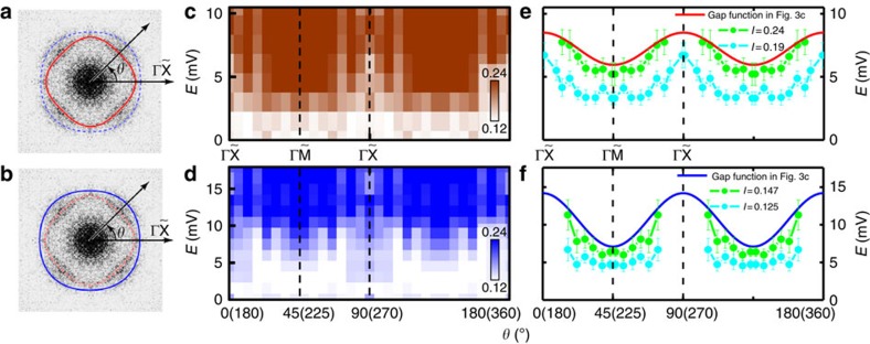
forms an outer circle. When we take the ρ(q, E)
intensity along the contours of the inner and outer rings as shown in Fig. 7a,b, an angle-dependent
ρ(θ, E) at various energies can be
obtained and presented in Fig. 7c,d as the 2D colour
plots. The 2D colour plots of ρ(θ, E)
along the inner and the outer rings both show the fourfold symmetry. The
line-cut of QPI intensity versus q along the radial direction at several
angles is shown in Supplementary Fig.
5. The low or null intensity of ρ(θ,
E) near the
  direction along each ring
may be induced by the band-crossing effect, or suggest that the Fermi surface in
this part is still gapped, so both minima of the gaps appear in the
  directions. To illustrate it more clearly, we take the
vertical line-cuts on the colour plot and show in Fig.
7e,f the angle-dependent energy thresholds at two certain FT-QPI
intensities along the inner and outer rings. Considering the two anisotropic
s-wave gap functions derived in the Dynes model fitting to the
measured STS spectrum, we put the angle-dependent gap functions, as shown by the
solid lines in Fig. 7e,f, onto the vertical line-cut data
(shown by the symbols) at two certain ρ(θ,
E) intensities (I=0.19, 0.24 and
I=0.125, 0.147 for the inner and outer rings, respectively).
If taking the values of I=0.24 and 0.147 as the rough
criterion for the gaps on the inner and outer pockets, one can see that the gap
functions follow those derived from the Dynes model fitting pretty well. Both
gap minima on the two circles appear in the
  directions, which is consistent with the direction of gap minima of electron
pockets in FeSe0.45Te0.55 (ref. 34). In the narrow region along the
  direction, since the intensity is very low and the uncertainty is
quite large, we are not able to derive the reliable gap values. Through above
analysis and discussions, we can assign the larger (smaller) gap
Δ1 (Δ2) to the outer (inner) Fermi
surfaces, which form two circles in the FT-QPI pattern in the
q-space.
Figure 6. The evolution of FT-QPI intensity ρ (q, E ) at different energies.
(a–j) The FT-QPI ρ(q, E) images are derived from Fourier transformation on the QPI images with the real-space scale of 58 nm × 58 nm. A 2D-gaussian-function background was subtracted from the raw FT-QPI image and the fourfold symmetrization was carried out to enhance the signal. The intensity on the inner ring in q-space shows up at above 3.5 mV, the ring becomes clear at the energy of the smaller gap, namely 8.6 mV, while the segments corresponding to the outer ring appear gradually with a higher energy above 6.8 mV, and are clear when measuring with the voltage at the larger energy gap 14.5 mV.
Figure 7. 2D colour plots of FT-QPI intensity ρ(θ, E) along the inner and outer contours of the central pattern in q-space.
(a,b) The FT-QPI pattern taken at 14.5 mV. The
solid-line contours in a and b were expressed approximatively
by R1−r1cos4θ
and R2+r2cos4θ
for outer and inner rings, respectively. (c,d) The FT-QPI
intensity along the inner (a) and outer (b) rings at different
angles taken from the fourfold symmetrized FT-QPI patterns in Fig. 6 with various energy values. The initial polar angle
starts from the  direction. The gap minimum
locates in the
  direction for both contours.
(e,f) The angle-dependent energy thresholds taken from the
vertical line-cuts to the colour plots in c,d by using the
intensity I=0.19, 0.24 (0.125, 0.147) for the inner
(outer) rings in a,b, respectively. The gap minimum locates in
the
  direction for both contours. The solid
lines in e,f plots are the gap functions derived from the
Dynes model fitting to the spectrum taken at 1.5 K. The error
bars were determined from the deviations between the line-cut experimental
data and the polynomial fitting curve for each angle.
Discussion
Concerning the two-gap functions with different maximum magnitudes derived from the
fitting to both STS spectra and the emergence of two sets of rings in the FT-QPI
images, we would like to put forward the picture concerning the band folding
(perhaps also hybridization) of the two electron pockets in the folded BZ, as shown
in Fig. 5d. In iron-based superconductors, the electron
pockets are usually elliptic-shaped and then fold (perhaps also by hybridization) in
the folded BZ with two Fe atoms in one unit cell. On the single elliptic Fermi
surface, the segments in the pole region are contributed by the
dxy orbitals, while the waist areas are derived
from the dxz/dyz orbitals35. Due to the folding effect, we have two sets of Fermi pockets which
correspond well to the inner
(dxz/dyz) and outer
(dxy) pockets. The crossing area consists of
electrons with mixed orbitals of dxy and
dxz/dyz. This may be the
reason why JDOS is very weak between the overlapped Fermi surfaces and the outer
ring seems not to close completely in the  directions.
The anisotropic FT-QPI intensity has been self-consistently explained as the cause
of the gap anisotropy in present study. While it may also be influenced by (or
partly related to) the variations in the orbital character of the bands around a
given energy contour25,29,31, and the unclosed part along
 directions mentioned above may give such
suggestion. We cannot rule out the effect of the anisotropic orbital character to
the anisotropic FT-QPI patterns. Another possible reason for the anisotropic FT-QPI
intensity is the anisotropic self-energy, which can affect the FT-QPI pattern,
especially when the measuring energy is above the superconducting gap36. In the low energy FT-QPI, such effect may also appear together with the
anisotropic superconducting gap36, although this could be a much
weaker effect. Since the anisotropic-gap function is strongly tied with the
anisotropic orbital character and self-energy effect, it will be important to figure
out which factor is the dominant role for inducing the anisotropic FT-QPI intensity,
especially in the energy region above the larger gap. We must emphasize that all
these possible alternatives do not change the major results in this study, that is,
the identifying of the double electron pockets near
  point and the associated double gaps. If the nodeless d-wave is applicable in
the system, sign reversal of superconducting gaps should exist between two
neighbouring elliptic Fermi pockets. In this case, in the band folding (perhaps also
hybridized) region, the gap should be zero, which is not consistent with our
results. In this picture with electron pocket folding, our data indicate a smaller
gap in the inner pocket with the
dxz/dyz characteristic, while
the larger gap accommodates in the outer pocket with the
dxy characteristic. To our knowledge, this is the first
time to resolve the two sets of Fermi pockets and associated gaps near the
 point. In the situation of s-wave gap
on the hybridized electron pockets, the theoretically predicted gap maximum locates
in the
  directions and gap minimum locates in the
 directions13, which is
consistent with our results. Although we cannot recognize that the gap maxima locate
in the
  directions just from the intensity plot of
FT-QPI in Fig. 7c–f, however, the tunnelling
spectrum shows fully gaped feature near zero-bias together with a fourfold angle
dependence of the gap, the FT-QPI shows also a fourfold feature and the gap minimum
locates in the
  directions. All these strongly suggest
that the gap distribution may be very similar to the situation shown in Fig. 7c–f. Further ARPES experiments with refined
resolution are strongly desired to confirm the conclusions derived here. In
addition, our results here resolve two sets of Fermi pockets and associated gaps,
which provides a very good stage for further checking whether there are sign
reversal gaps between the inner and outer folded (or hybridized) Fermi pockets. This
is actually underway by following the recent theoretical predictions37. That should be very crucial for a final pinning down of the repulsive
interaction-induced pairing. Our observation of two superconducting gaps and the
assignment of the two gaps to the folded (or hybridized) two sets of Fermi pockets
in the new superconductor
(Li1−xFex)OHFeSe is very intriguing.
Furthermore, the huge gap ratio
2Δ1/kBTc=8.7
indicates the strong coupling mechanism for superconductivity in the iron-based
superconductors.
Methods
Sample synthesis and characterization
The (Li1−xFex)OHFeSe single crystals were synthesized by the hydrothermal ion-exchange method7. First, 6 g LiOH (J&K, 99% purity) was dissolved in 15 ml deionized water in a teflon-linked stainless-steel autoclave (volume 50 ml). Then, 0.6 g iron powder (Aladdin Industrial, 99% purity), 0.3 g selenourea (Alfa Aesar, 99% purity) and several pieces of K0.8Fe2−xSe2 single crystals were added to the solution. After that, the autoclave was sealed and heated up to 120 °C followed by staying for 40 to 50 h. Finally, the (Li1−xFex)OHFeSe single crystals can be obtained by leaching. The DC magnetization measurement was carried out with a SQUID-VSM-7T (Quantum Design) with a resolution of 5 × 10⁻⁸ e.m.u. The resistivity measurement was done on a PPMS-16T (Quantum Design) with the standard four-probe method.
STM/STS measurements
The STS spectra were measured with an ultra-high vacuum, low-temperature and high-magnetic field scanning tunnelling microscope (USM-1300, Unisoku Co., Ltd.). The samples were cleaved in an ultra-high vacuum with a base pressure about 1 × 10⁻¹⁰ torr. During all STM/STS measurements, tungsten tips were used. To lower down the noise of the differential conductance spectra, a lock-in technique with an ac modulation of 0.8 mV at 987.5 Hz was used.
Additional information
How to cite this article: Du, Z. et al. Scrutinizing the double superconducting gaps and strong coupling pairing in (Li1−xFex)OHFeSe. Nat. Commun. 7:10565 doi: 10.1038/ncomms10565 (2016).
Supplementary Material
Supplementary Figures 1-5, Supplementary Table 1 and Supplementary Notes 1-3
Acknowledgments
We acknowledge the useful discussions with Qianghua Wang, Jiangping Hu and Dunghai Lee. This work was supported by the National Natural Science Foundation of China (Grant No. 11534005, No.11190023), the Ministry of Science and Technology of China (973 projects: 2011CBA00100, 2012CB821403) and PAPD.
Footnotes
Author contributions The low-temperature STS measurements were finished by Z.D., X.Y., D.F., G.D., H.Y. and H.-H.W. The samples were prepared by H.L. and X.Z. The data analysis was done by Z.D., X.Y., D.F. and H.Y. H.-H.W. coordinated the whole work. H.Y. and H.-H.W. wrote the manuscript which was supplemented by others. All authors have discussed the results and the interpretation.
References
- Wang Q. Y. et al. Interface-induced high-temperature superconductivity in single unit-cell FeSe films on SrTiO3. Chin. Phys. Lett. 29, 037402 (2012). [Google Scholar]
- Lee J. J. et al. Interfacial mode coupling as the origin of the enhancement of Tc in FeSe films on SrTiO3. Nature 515, 245–248 (2014). [DOI] [PubMed] [Google Scholar]
- He S. L. et al. Phase diagram and electronic indication of high-temperature superconductivity at 65 K in single-layer FeSe films. Nat. Mater. 12, 605–610 (2013). [DOI] [PubMed] [Google Scholar]
- Tan S. Y. et al. Interface-induced superconductivity and strain-dependent spin density waves in FeSe/SrTiO3 thin films. Nat. Mater. 12, 634–640 (2013). [DOI] [PubMed] [Google Scholar]
- Lu X. F. et al. Coexistence of superconductivity and antiferromagnetism in (Li0.8Fe0.2)OHFeSe. Nat. Mater. 14, 325–329 (2015). [DOI] [PubMed] [Google Scholar]
- Pachmayr U. et al. Coexistence of 3d-Ferromagnetism and Superconductivity in [(Li1−xFex)OH](Fe1−yLiy)Se. Angew. Chem. Int. Ed. 54, 293–297 (2015). [DOI] [PubMed] [Google Scholar]
- Dong X. L. et al. (Li0.84Fe0.16)OHFe0. 98Se superconductor: Ion-exchange synthesis of large single-crystal and highly two-dimensional electron properties. Phys. Rev. B 92, 064515 (2015). [Google Scholar]
- Rotter M., Tegel M. & Johrendt D. Superconductivity at 38 K in the Iron Arsenide (Ba1−xKx)Fe2As2. Phys. Rev. Lett. 101, 107006 (2008). [DOI] [PubMed] [Google Scholar]
- Chen G. F., Hu W. Z., Luo J. L. & Wang N. L. Multiple phase transitions in single-crystalline Na1-δFeAs. Phys. Rev. Lett. 102, 227004 (2009). [DOI] [PubMed] [Google Scholar]
- Hsu F. C. et al. Superconductivity in the PbO-type structure α-FeSe. Proc. Natl Acad. Sci. USA 105, 14262–14264 (2008). [DOI] [PMC free article] [PubMed] [Google Scholar]
- Mazin I. I., Singh D. J., Johannes M. D. & Du M. H. Unconventional superconductivity with a sign reversal in the order parameter of LaFeAsO1−xFx. Phys. Rev. Lett. 101, 057003 (2008). [DOI] [PubMed] [Google Scholar]
- Kuroki K. et al. Unconventional pairing originating from the disconnected Fermi surfaces of superconducting LaFeAsO1−xFx. Phys. Rev. Lett. 101, 087004 (2008). [DOI] [PubMed] [Google Scholar]
- Khodas M. & Chubukov A.V. Interpocket pairing and gap symmetry in Fe-based superconductors with only electron pockets. Phys. Rev. Lett. 108, 247003 (2012). [DOI] [PubMed] [Google Scholar]
- Zhao L. et al. Common electronic origin of superconductivity in (Li,Fe)OHFeSe bulk superconductor and single-layer FeSe/SrTiO3 films. Preprint at http://arxiv.org/abs/1505.06361 (2015). [DOI] [PMC free article] [PubMed]
- Niu X. H. et al. Surface electronic structure and isotropic superconducting gap in (Li0.8Fe0.2)OHFeSe. Phys. Rev. B 92, 060504 (2015). [Google Scholar]
- Bean C. P. Magnetization of high-field superconductors. Rev. Mod. Phys. 36, 31–39 (1964). [Google Scholar]
- Shen B. et al. Intrinsic percolative superconductivity in KxFe2−ySe2 single crystals. Europhys. Lett. 96, 37010 (2011). [Google Scholar]
- Fischer Ø., Kugler M., Maggio-Aprile I., Berthod C. & Renner C. Scanning tunneling Spectroscopy of high-temperature superconductors. Rev. Mod. Phys. 79, 353–419 (2007). [Google Scholar]
- Hanaguri T., Niitaka S., Kuroki K. & Kakagi H. Unconventional s-wave superconductivity in Fe(Se,Te). Science 328, 474–476 (2010). [DOI] [PubMed] [Google Scholar]
- Hoffman J. E. Spectroscopic scanning tunneling microscopy insights into Fe-based superconductors. Rep. Prog. Phys. 74, 124513 (2011). [Google Scholar]
- Yang H. et al. In-gap quasiparticle excitations induced by non-magnetic Cu impurities in Na(Fe0.96Co0.03Cu0.01)As revealed by scanning tunnelling spectroscopy. Nat. Commun. 4, 2749 (2013). [DOI] [PMC free article] [PubMed] [Google Scholar]
- Yang H. et al. Unexpected weak spatial variation in the local density of states induced by individual Co impurity atoms in superconducting Na(Fe1−xCox)As crystals revealed by scanning tunneling spectroscopy. Phys. Rev. B 86, 214512 (2012). [Google Scholar]
- Chi S. et al. Scanning tunneling spectroscopy of superconducting LiFeAs single crystals: evidence for two nodeless energy gaps and coupling to a bosonic mode. Phys. Rev. Lett. 109, 087002 (2012). [DOI] [PubMed] [Google Scholar]
- Hänke T. et al. Probing the unconventional superconducting state of LiFeAs by quasiparticle interference. Phys. Rev. Lett. 108, 127001 (2012). [DOI] [PubMed] [Google Scholar]
- Chi S. et al. Sign inversion in the superconducting order parameter of LiFeAs inferred from Bogoliubov quasiparticle interference. Phys. Rev. B 89, 104522 (2014). [Google Scholar]
- Lang M. K. et al. Imaging the granular structure of high-Tc superconductivity in underdoped Bi2Sr2CaCu2O8+δ. Nature 415, 412–416 (2002). [DOI] [PubMed] [Google Scholar]
- Yazdani A., Howald C. M., Lutz C. P., Kapitulnik A. & Eigler D. M. Impurity-induced bound excitations on the surface of Bi2Sr2CaCu2O8. Phys. Rev. Lett. 83, 176–179 (1999). [Google Scholar]
- Dynes R. C., Narayanamurti V. & Garno J. Pm. Direct measurement of quasiparticle-lifetime broadening in a strong-coupled superconductor. Phys. Rev. Lett. 41, 1509–1512 (1978). [Google Scholar]
- Huang D. et al. Nanoscale imaging of orbital texture in single-layer FeSe/SrTiO3. Preprint at http://arxiv.org/abs/1509.07110 (2015).
- Lee D.-H. What makes the Tc of FeSe/SrTiO3 so high? Chin. Phys. B 24, 117405 (2015). [Google Scholar]
- Zhang Y. Y. et al. Quasiparticle scattering interference in superconducting iron pnictides. Phys. Rev. B 80, 094528 (2009). [Google Scholar]
- Akbari A., Knolle J., Eremin I. & Moessner R. Quasiparticle interference in iron-based superconductors. Phys. Rev. B 82, 224506 (2010). [DOI] [PubMed] [Google Scholar]
- Allan M. P. et al. Anisotropic energy gaps of iron-based superconductivity from intraband quasiparticle interference in LiFeAs. Science 336, 563–567 (2012). [DOI] [PubMed] [Google Scholar]
- Zeng B. et al. Anisotropic structure of the order parameter in FeSe0.45Te0.55 revealed by angle-resolved specific heat. Nat. Commun. 1, 112 (2010). [DOI] [PMC free article] [PubMed] [Google Scholar]
- Hirschfeld P. J., Korshunov M. M. & Mazin I. I. Gap symmetry and structure of Fe-based superconductors. Rep. Prog. Phys. 74, 124508 (2011). [Google Scholar]
- Allan M. P. et al. Identifying the 'fingerprint' of antiferromagnetic spin fluctuations in iron pnictide superconductors. Nat. Phys. 11, 177–182 (2015). [Google Scholar]
- Hirschfeld P. J., Altenfeld D., Eremin I. & Mazin I. I. Robust determination of superconducting gap sign changes via quasiparticle interference. Phys. Rev. B 92, 184513 (2015). [Google Scholar]
Associated Data
This section collects any data citations, data availability statements, or supplementary materials included in this article.
Supplementary Materials
Supplementary Figures 1-5, Supplementary Table 1 and Supplementary Notes 1-3


