Abstract
Purpose
We tested the feasibility of implementing parallel transmission (pTX) for high field MRI using a radiofrequency (RF) amplifier design to be located on or in the immediate vicinity of a RF transmit coil.
Method
We designed a current-source switch-mode amplifier based on miniaturized, non-magnetic electronics. Optical RF carrier and envelope signals to control the amplifier were derived, through a custom-built interface, from the RF source accessible in the scanner control. Amplifier performance was tested by benchtop measurements as well as with imaging at 7 T (300 MHz) and 11.7 T (500 MHz). The ability to perform pTX was evaluated by measuring inter-channel coupling and phase adjustment in a 2-channel setup.
Results
The amplifier delivered in excess of 44 W RF power and caused minimal interference with MRI. The interface derived accurate optical control signals with carrier frequencies ranging from 64 to 750 MHz. Decoupling better than 14 dB was obtained between 2 coil loops separated by only 1 cm. Application to MRI was demonstrated by acquiring artifact-free images at 7 T and 11.7 T.
Conclusion
An optically controlled miniaturized RF amplifier for on-coil implementation at high field is demonstrated that should facilitate implementation of high-density pTX arrays.
Keywords: parallel transmission, high field MRI, RF amplifiers
Introduction
High field (≥ 7 T) MRI of the brain has yielded increased contrast, sensitivity, and resolution (1). Unfortunately, wavelength effects typical at high field compromise B1 homogeneity, and can degrade image quality. Several methods (2–5) have been proposed to mitigate this problem, often by using multiple RF transmitters. However, the use of multiple transmitters at high field presents various technical difficulties, including safe and independent control of the individual transmit fields in the presence of significant inter-channel coupling and the complex interaction of the transmit elements (e.g. conductor strips or coils) with the object. In order to address these difficulties, a re-design of the RF transmit system seems warranted.
One of the problems with conventional RF transmission in MRI is that, due to its physical size and magnetic interference, the RF amplifier needs to be placed at a distance from the transmission element(s) in the MRI scanner. This increases the difficulty to accurately control and monitor the amplitude and phase of the RF currents delivered to the transmit elements, and to avoid coupling between elements. To mitigate these problems, various novel RF amplification approaches have been proposed. Inspired by the active rung concept introduced by Kurpad et al. (6), voltage-controlled current-source amplification integrated with the transmit conductor has been proposed as a way to control transmitted fields under conditions of electrical and magnetic coupling between nearby transmit elements and of variable RF absorption by the object (7,8). However, this approach brings new technical challenges such as assuring compatibility with the magnetic field and low power dissipation from the additional in-bore electronics. Further complications relate to cabling setup and the integration of the amplifier control with the scanner hardware.
An optimization of the current-drive approach has been presented in the implementation of a 64 MHz four-channel transmit array built from switch-mode current-source amplifiers to be located near or on the coil (9). Switch-mode (non-linear) operation of the output field-effect transistors (FETs) through a current-mode class-D (CMCD) topology (10) has been shown to minimize power dissipation on the amplifier board. This allows operation at high duty cycle without the need for heat sinks or forced-air cooling (11). By digitizing the amplifier input signals, coaxial cables could be replaced by optical fibers, eliminating any possibility of RF interference across parallel connections (9,12). However, two remaining issues with this implementation were the slight magnetization of some electronics components, which required placing the amplifier prototype 20 cm away from the coil (and object) to avoid magnetic susceptibility artifacts, and lack of integration with the scanner system.
A miniaturized non-magnetic CMCD amplifier based on an ultra-small package enhancement-mode gallium nitride (eGaN) FETs was demonstrated for 64 MHz operation (13). We adopted similar FET technology to miniaturize current-source amplifiers for on-coil operation at 300 MHz (14) and 500 MHz. To facilitate integration with the MRI scanner, we developed a modular multiple-channel optical interface that allows operation over a wide range of MR-frequencies. The proposed amplifier-interface combination furthermore incorporates optically monitoring of the coil current amplitude, which will be critical to assure safe operation within the limits of allowable tissue heating.
Methods
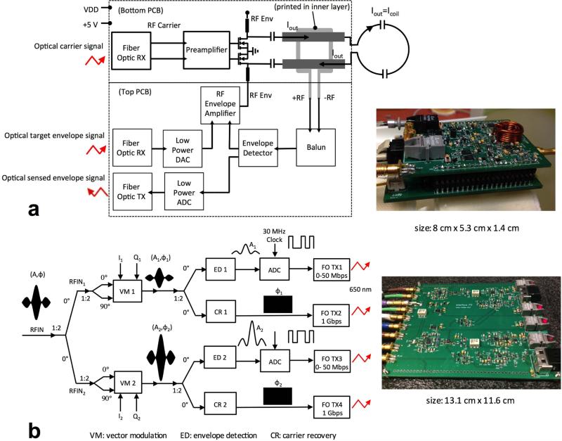
Our RF transmit setup included an optical drive interface and switch-mode current source amplifiers to be located at the transmit coil. The optical interface extracted the RF excitation pulse waveform from the scanner control cabinet (normally supplied to the conventional RF power amplifier), recovered its envelope and carrier information, and converted these signals into two digital optical signals. These optical signals were then supplied to the amplifiers. A modular approach was used, with each module containing a two-channel optical drive (two optical carriers and two optical envelope signals) controlling two amplifiers. Each amplifier consisted of a RF carrier amplifier board and a separate plug-in envelope amplifier board connected on the top (Fig. 1a). The amplified envelope signal modulated the drain voltage of the FETs at the carrier amplifier output stage (CMCD) to generate high power shaped RF pulses (15).
Figure 1.
Simplified diagram and photograph of the high field on-coil current-source amplifier and optical pTX interface. (a) The amplifier is controlled by two optical signals: a carrier and an envelope. A third optical signal is derived from a B1/current sensing loop and returned for monitoring purposes. (b) In a first stage, two RF pulses of different amplitudes and phases can be generated from a single RF input pulse. In a second stage, the envelope and carrier information are recovered separately, digitized, and optically transmitted to the on-coil amplifiers located in the magnet bore.
Amplifier design
Our amplifier prototype (Fig. 1a) replaced the large and slightly magnetic metal oxide semiconductor FETs (MOSFETs) of the original design (9,16) with miniature non-magnetic eGaN FETs as previously done for an optimized 64 MHz on-coil CMCD amplifier prototype (13). These eGaN FETs require a relatively low gate voltage to switch, but as switching frequency is increased more peak current is required from the driver to charge the port capacitances. To switch the eGaN FETs (EPC8010, 100 V, 2.7 A, Rds_ON=0.16 Ω) at 300 MHz and above, the small carrier signal at the output of the 1 Gbps fiber optic transceiver (FOTX-RX FB01GLVR, Firecomms, Cork, Ireland) was pre-amplified using a pair of small power broadband monolithic amplifiers (ERA; Mini-Circuits, Brooklyn, New York, USA). These were used to drive a pair of N-channel MOSFETs (2SK2854; Toshiba,Tokyo, Japan) in push-pull class-D configuration. By tuning the matching network at the gate of the N-MOSFETs, the preamplifier drove enough voltage and current at both 300 MHz and 500 MHz. As in the previous design, the high power CMCD stage had an output filter that improved efficiency and provided decoupling to neighboring transmit elements by resonating the FET's output capacitance Cd (9,11). The amplifier prototype was built on a four-layer printed circuit board (PCB) with dimensions of 8 × 5.3 cm2. To track the current in the coil (17,18), a rectangular loop of dimensions 7.5 × 6.5 mm2 was printed in the first inner layer (from the top) of the PCB and positioned beneath the output traces of the amplifier (Fig.1a). This implementation is possible due to the direct connection between the amplifier and the coil (no matching network in between).
The envelope amplifier consisted of a PWM controlled buck converter with the duty cycle set by the difference between a target envelope (envelope input) and the sensed envelope, as was done previously (9). The target envelope was recovered, after optical reception, by an ultra-low power (10 mW) 6-pin digital-to-analog converter (DAC) (AD5611; Analog Devices, Norwood, Massachusetts, USA). The sensed envelope was recovered by an envelope detector (ADL5511, Analog Devices) connected through a balun to the terminals of the rectangular current loop integrated in the RF amplifier board (Fig. 1a). The envelope detector also provided a separate root-mean-square (rms) voltage output that tracked the envelope of the input signal; this voltage was digitized through an ultra-low power analog-to-digital converter (ADC, AD7277, Analog Devices) to allow optical transmission to the scanner console as a means to monitor coil current (Fig. 1a). The envelope amplifier and current monitoring circuit were built in a 6-layer PCB with dimensions 7.1 × 5.3 cm2. With both boards connected, the size of the amplifier was 8 cm × 5.3 cm × 1.4 cm (length × width × height)
Optical interface design
The amplifier was fed by two separate optical signals: the RF carrier and the envelope. The interface board was designed to generate the necessary optical signals for multiple amplifiers from a single RF signal available in the scanner control cabinet. As demonstrated previously in an implementation of a pTX interface to control remote (but not on-coil) linear amplifiers (19,20), amplitudes and phases for multiple transmitters can be derived from a single RF input by use of vector modulators. A similar approach was followed here to supply the signals for 2 transmitters (Fig. 1b). The RF signal was first fed into a two-way 0° power splitter (ADP-2-1W, Minicircuits), whose signals were fed into two-way 90° power splitters (QCN-5D, Minicircuits); this generated the quadrature inputs to a pair of vector modulators (ADL5390, Analog Devices). Two RF pulses of same shape but with controllable amplitude and phase were generated at the output of the modulators. Amplitudes and phases were set through the in-phase (I) and quadrature (Q) baseband control signals of the modulators. These signals were generated by a PCI board (PCI-6723; National Instruments, Austin, Texas, USA), installed in a peripheral computer and controlled through a custom user interface. Each of the RF pulses was split one more time to feed a carrier recovery (CR) circuit formed by a high-speed comparator (ADCMP572, Analog Devices) in a zero-detection configuration and a high bandwidth envelope detection (ED) circuitry (ADL5511, Analog Devices) followed by a low power ADC clocked at 30 MHz (generated externally from a master clock board). The digital envelope and carrier signals were then transmitted through fiber optic transmitters to control the amplifier. The carrier was transmitted using a 1 Gbps optical converter (FOTX-RX FB01GLVR, Firecomms) and the encoded envelope was transmitted through a 50 Mbps(AFBR-1624Z; Avago, San Jose, California, USA). The 30 MHz clock and synchronization signals necessary for the digital demodulation on the amplifier board were also sent optically from the interface through the 50 Mbps converters (not shown in simplified diagram of Fig. 1b). These signals were received on a 1:4 clock distribution board located in the scanner room (next to the amplifiers) and designed to control up to four amplifiers simultaneously. Mounting of additional interface modules (on top of the 2-channel master module shown in photograph of Fig. 1b) was made possible through a 40-pin connector, from which DC power and the RF unblank signal were supplied (most of the remaining pins supplied signal ground).
Benchtop and MRI Measurements
The gain of the carrier pre-amplification stage was tested; enough gain at both frequencies is essential to switch the eGaN FETs efficiently for imaging at 7 T and 11.7 T using same amplifier design. Amplifier power and current delivered to the coil were measured while efficient switching of the power FETs was evaluated by temperature measurements performed with the FETs driving close to their specified maximum current. Load sensitivity and inter-channel decoupling were measured and the envelope bandwidth and dynamic range generated by the interface-amplifier system were estimated.
Amplifier benchtop testing
The voltage gain of the pre-amplification stage was determined from the ratio between the peak voltage at the gate of the eGaN FETs and the peak voltage at the output of the optical receiver (RX) for both 300 and 500 MHz. Each amplifier was connected to a transmit element, which consisted of a 6 cm diameter coil tuned at 300 MHz by seven distributed capacitors with values between 11 pF to 12 pF. To avoid possible susceptibility artifacts, the amplifier was separated from the sample by a 7.5 cm RG316 coaxial cable connection to the coil. Coil and cable were resonated to have pure resistive impedance at the amplifier output. Coils were loaded either with a rectangular 4.7 L oil phantom or with a cylindrical 4.5 L Sucrose-NaCl gel phantom. The sucrose phantom mimicked the dielectric properties of average brain tissue at 300 MHz (21). A 1.1 cm spacing between phantom and loop was maintained by using a plastic, RF-transparent spacer. Oil and sucrose phantom presented a load of 1.3 and 7 Ω respectively at the output of the amplifier when the loops were slightly retuned to cancel any reactive impedance. B1 field, output current and output power were estimated by using a 2.2 cm diameter field probe calibrated at 2.07 μT/V (confirmed by subsequent B1+ mapping) when the amplifier was loaded with 7 Ω approximately (sucrose phantom). The heat dissipation on the amplifier board was evaluated with infrared thermal imaging (E40 Thermal Camera; FLIR Systems, Wilsonville, Oregon, USA) after 2-minute operation of the amplifier close to its maximum current (~2.7 A in the 7 Ω load) at a 10% duty cycle.
The load sensitivity of the amplifier was tested by changing the distance between the loop and the sucrose phantom while measuring the B1 field at the center of the loop. The distance was adjusted incrementally by stacking rigid spacers between coil and phantom. This allowed the load to be varied between 1.5 Ω (unloaded) and 16 Ω (sucrose phantom without spacer).
The effect of the amplifier output impedance on currents induced by neighboring elements was evaluated by placing two adjacent loops separated by 1 cm gap and coupled to the oil phantom. One of the loops was connected to an amplifier in a passive state (with drain bias but not transmitting RF), while the other loop was connected directly to the port of a network analyzer (NA) presenting a 50 Ω load [7,9]. In order to evaluate the effect of the amplifier output impedance in isolation, the current feedback was disabled by disconnecting the envelope amplifier board from the CMCD amplifier. Transmission coefficient S21 was measured for different drain bias voltages by sending power from port 1 of the NA into the connected loop and receiving power in port 2 through a probe sensing the field in the loop connected to the amplifier.
Interface benchtop testing
First, to evaluate the broadband behavior of the interface, the recovered carrier signal was measured on the amplifier board for various frequencies (64-750 MHz) of the carrier supplied to the interface board. A signal generator (SML01, 9 kHz to 1.1 GHz; Rohde & Schwarz, Munich, Germany) supplied the carrier signal; the recovered carrier was measured with a 3.5 GHz active differential probe (N2751A InfiniiMode; Keysight, Santa Rosa, California, USA). The amplitude of the fundamental component was measured for input and output signals with the FFT function of the oscilloscope to calculate the gain.
To measure the performance of amplitude modulation, the modulation input of the signal generator was connected to a function generator (Agilent 33250A) to obtain 297.2 MHz sinusoidal modulated pulses of different amplitudes and frequencies. Dynamic range was estimated as the ratio between maximum and minimum detectable peak voltages measured at the DAC output, located on the amplifier board, while envelope bandwidth was estimated based on the −3 dB criterion. Linearity was evaluated by measuring the intermodulation products at the DAC output when two tones at 15 and 18 kHz (with the 297.2 MHz carrier) were supplied to the interface.
Testing of coil current monitoring feature
To test the performance of the coil current monitoring system, the optical output on the amplifier board was connected through a 1-m fiber to a remote PCB that included an optical RX followed by a DAC. The DAC output was monitored with the oscilloscope while controlling the B1 amplitude by setting different values for the I and Q control signals of the modulators through the user interface. B1 amplitude was measured simultaneously through the calibrated probe coupled to the transmit (TX) loop and connected to the oscilloscope.
MRI experiments
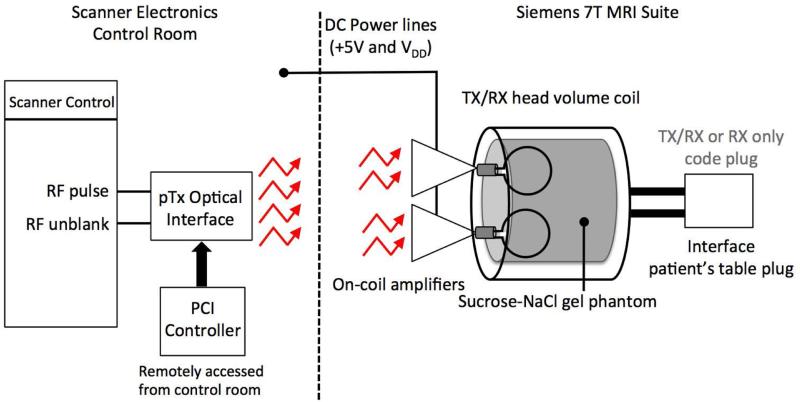
Once placed in the scanner, the amplifiers were connected via 10-m long fiber-optic cables to the optical interface located in the scanner equipment room (Fig. 2). The RF pulse and the RF unblank signals from the scanner control were connected as inputs to the interface. RF phase and amplitude of each transmit channel were dynamically controlled through the baseband signals of the modulators sent from the PCI board located also in the equipment room but accessed remotely from a PC in the scanner control room. The amplifiers were powered with only 2 supplies, +5 V line and a higher voltage line (VDD) adjusted up to 25 V, both connected through a penetration panel in the scanner's RF shield. For signal reception, a custom-built head volume coil (22) was used in RX mode.
Figure 2.
System setup in a 7 T MRI scanner. The optical interface was connected to the low power RF pulse and RF unblank signals accessible in the scanner control cabinet. The computer with the PCI board to control it was remotely accessed from the MRI control room. Optical signals were transmitted through 10 m long fibers to the on-coil amplifiers located inside the bore. A head volume coil was used for signal reception.
To test for susceptibility effects introduced by the implemented prototype, reference images of a spherical oil phantom were first acquired with a head volume coil (Nova Medical, Wilmington, Massachusetts, USA) without the amplifier situated inside the bore. Next, images of the oil phantom were acquired with the amplifier located at different distances from the phantom. For both measurements, a multi-slice multi-echo gradient echo (GRE) sequence was used with default shim settings. Frequency maps were reconstructed from the acquired data to check for effects of the amplifiers on the magnetic field. Imaging acquisition parameters were: 192 × 192 mm2 in plane field-of-view (FOV), 3 × 3 × 3 mm3 resolution, 1 s repetition time (TR), six echoes (TEMIN=3.01 ms, TEMAX=12.06 ms and TESTEP= 1.81 ms), 64 s acquisition time (TA) and 80° nominal flip angle.
To test the overall system (interface-amplifier) linearity, slice profile images were acquired with a single loop with a 2D GRE sequence, orienting the read-gradient in the direction of the slice-select gradient. As a control experiment, slice profiles were also measured with a conventional transmit setup consisting of a linear amplifier (Mini-Circuits, LZY-1, 50 W 20 to 512 MHz) remotely connected to a transmit loop. For excitation, 1 ms windowed (Hamming) sinc pulses of different bandwidths (by changing the number of zero-crossings) were used. 2D GRE was used with 300 × 300 mm2 FOV, 1.2 × 1.2 mm2 resolution, 10 mm slice thickness, 50 ms TR, 5 ms TE and 4 signal averages.
Inter-channel coupling was evaluated with two 6 cm loop coils (tuned to 300 MHz) placed together with the oil phantom. The coils were separated from each other by 1 cm and separated from the phantom by 1.1 cm (as in the benchtop decoupling measurement). B1+ maps were acquired with a modified Bloch-Siegert method (23); both when transmitting through each channel separately and then also simultaneously while varying their relative phase. Maps were acquired with 192 × 192 mm2 FOV, 1.5 × 1.5 mm2 resolution, 5 mm slice thickness and 2 min TA. Average B1+ amplitude values in regions of interest (ROIs) at the center of each loop and midway between the loops were determined. The rationale for this measurement strategy, complementary to the benchtop measurement, was that in a fully decoupled setup, the combined B1+ of the 2 channels should be a linear summation of the B1 fields generated by the individual coils. Note, as in the benchtop measurements, this coupling test was performed without the amplitude feedback in place to evaluate the effect of amplifier impedance separately.
Dynamic phase control by the interface was further evaluated with the loops placed on opposing sides of the sucrose phantom. 2D GRE images were acquired while transmitting with various phase differences between the channels. MRI images were then compared with simulated B1+ profiles obtained from FDTD software (XFdtd 7.3; Remcom, State College, Pennsylvania, USA).
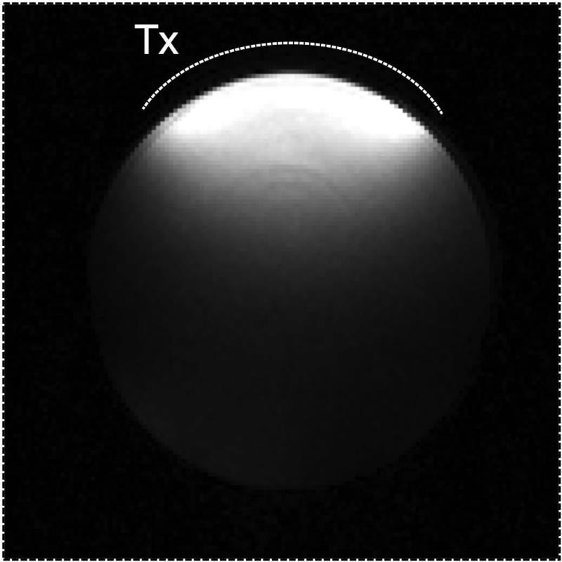
Finally, to evaluate operation at 500 MHz, one amplifier was connected (through the 7.5 cm coaxial cable) to a 4 cm diameter loop built from flexible PCB board, tuned at 500 MHz with three 1.6 pF capacitors and placed adjacent to a 250 ml oil phantom inside an 11.7 T scanner (31 cm horizontal bore scanner; Bruker, Billerica, Massachusetts, USA). A birdcage-type coil with 89 mm inner diameter and 11 cm length was used for signal reception. Images were acquired using GRE with a 1 ms RF pulse, 60 × 60 mm2 FOV, 0.5 × 0.5 mm2 resolution, 100 ms TR, 3.5 ms TE, and 8 averages.
Results
Amplifier benchtop performance
The preamplifier overall voltage gain was 25 dB at 300 MHz and 22 dB at 500 MHz respectively. The only adjustments needed for a change in operating frequency were to modify the component values of the matching networks at the gates of the N-FETs of the pre-amplification stage and at gates of the eGaN FETs of the power stage. The obtained voltage gain and a maximum allowable continuous current of 0.5 A were enough to effectively turn on and off the eGaN FETs at the CMCD stage.
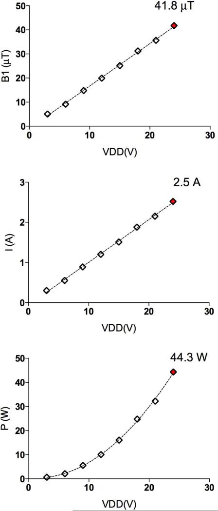
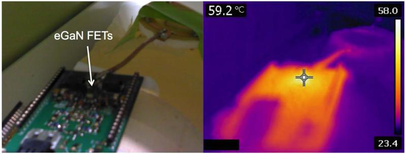
The dependencies of B1+ amplitude, output current and power on the amplifier bias voltage (CMCD stage bias) are shown in Fig. 3. We measured up to 42 μT at 1 cm distance from the coil, corresponding to an estimated 2.5 A peak current and 44 W peak output power at the coil. Operating at this power level at 10% duty cycle for 2 minutes, the highest temperature on the PCB was 59.2°C. As expected, this focal hot spot was near the eGaN FETs (Fig. 4).
Figure 3.
Measured B1 field, estimated amplifier output current (I) and power (P) when the amplifier was loaded with 7 Ω by coupling the loop with a sucrose phantom simulating brain tissue at 300 MHz.
Figure 4.
Photograph and infrared thermal image of amplifier board after two-minute operation at ~44 W and 10 % duty cycle. The mark indicates the location of the eGaN FET pair.
The B1 amplitude was stable to within 7 (±3)% with a factor of 10 of load variation. This shows the effectiveness of the current feedback in tracking the target RF envelope for a wide range of load values.
Decoupling between a 50 Ω-terminated loop and the amplifier-connected loop was better than 14 dB for all bias voltage conditions, confirming the low sensitivity of the amplifier setup to currents induced by neighboring transmitters.
Interface benchtop performance
The gain between the carrier signal recovered at the fiber RX on the amplifier side (top left in Fig. 1a) and the RF carrier input to the interface was greater than 2 dB across the entire 64-750 MHz frequency range and up to 7.6 dB at 300 MHz. Lower gain values (but still above 2 dB) resulted for the lower frequency range due to the higher impedance introduced by the multiple DC blocking capacitors in the RF carrier path. However, even these gains value would be high enough to drive the pre-amplification stage which would be optimized at the selected frequency of operation.
The resulting dynamic range and bandwidth of the envelope signal, recovered on the amplifier side, were 38 dB and 220 kHz respectively, which is sufficient for the majority of MRI applications. In the multi-tone experiment, intermodulation products were below −50 dB, which approached the noise floor of our measurement setup. This value is sufficiently low to be considered negligible (24), which indicates high linearity of the processed envelope signal. Envelope and carrier separation were successfully performed when the interface was connected to the control cabinet of the 7 T and 11.7 T systems.
Coil current monitoring through B1 feedback
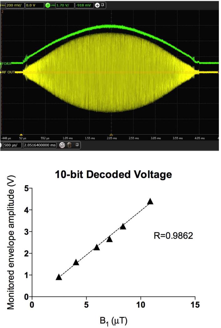
Figure 5 shows a shaped RF pulse measured at the amplifier output and its recovered envelope on the remote receiver board. The 10-bit decoded voltage for different B1 amplitudes is also shown. A gain of 0.41 V/μT was obtained for the current implementation, however this value can be modified by simple hardware adjustments to monitor higher B1 amplitudes without saturating the +5 V circuitry.
Figure 5.
Demonstration of current monitoring. RF output pulse and recovered envelope after optical reception and digital-to-analog conversion performed on the remote RX board (top). Decoded voltage versus B1 amplitude curve shows an approximate gain of 0.41 V/μT (bottom).
MRI experiments
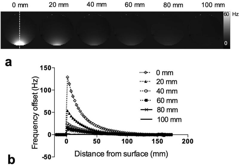
Conductive and magnetic properties of the amplifier were tested in the 7 T and 11.7 T scanner. No force was perceived when moving the amplifiers into the region of strong magnetic field. Figure 6 shows the frequency maps at the center slice for the different separations between the amplifier board and the surface of the spherical oil phantom (indicated on top). The plot shows the frequency profiles for the different setups in the center of the volume (bottom-top center line in each image in Fig. 6a). Frequency distortions were minimal for 40 mm separation and almost undetectable at 100 mm separation, suggesting minimal effect of the presented amplifier prototype on the static magnetic field.
Figure 6.
Magnetic field distortion caused by the on-coil amplifier, determined by measuring the B0 field change (inferred from resonance frequency) resulting from amplifier placement at various distances from the phantom. (a) Field distribution in an axial slice midway through a spherical oil phantom. The separation of the phantom and amplifier ranged from 0 to 100 mm, as indicated above the images. (b) Plots of the frequency offset on a line in the center of the volume (dashed line in panel a) for the various distance measurements.
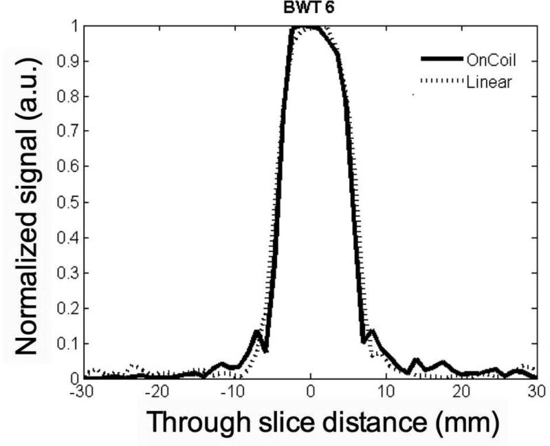
Slice profiles (Fig. 7) for the switch-mode current-source amplifier were similar to those of the reference (linear) amplifier, confirming preservation of the target envelope after the various signal manipulations. A small ringing artifact is observed in the profile obtained with our amplifier, which we attribute to minor RF leakage (~30 mA) through the gate-drain capacitance of the power FET. This is a common problem in RF CMCD amplifiers that can be solved by forcing the carrier amplitude to zero at the time the envelope signal is zero (9). In our implementation we expect to improve this by carefully designing a hysteresis window in the carrier recovery circuit of the interface.
Figure 7.
Demonstration of shaped pulse for slice selection (oil phantom). Profile intensity across the slice when transmitting with the remote linear amplifier, used as reference (dotted line) and with the on-coil switch-mode amplifier (solid line).
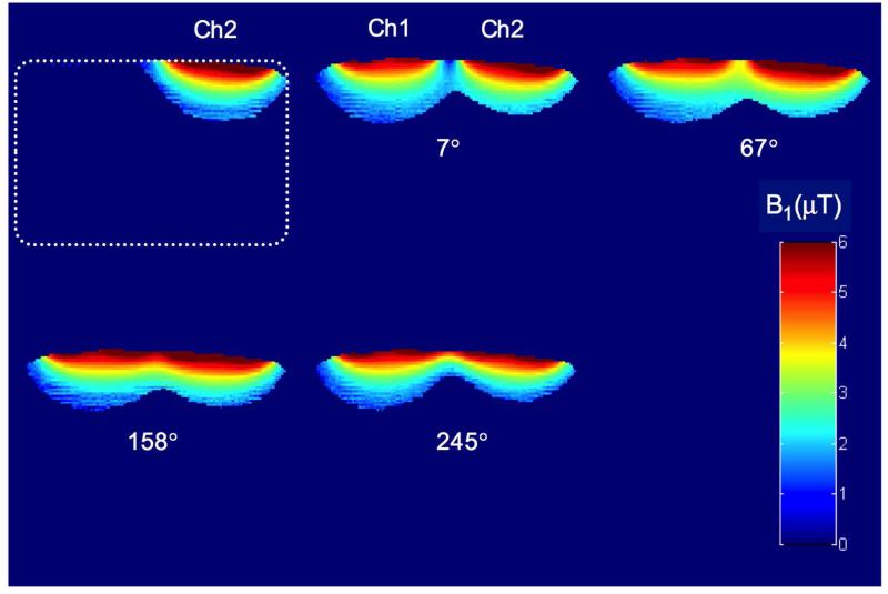
Examples of B1+ maps obtained during the inter-channel decoupling test are shown in Fig. 8 for single channel transmission and for two-channel transmission with various phase difference between channels. The minimal (~10%) change in B1+ amplitude at the center of each loop during variation of the B1 generated by the adjacent loops confirms the low coupling achieved with the on-coil amplifier design.
Figure 8.
Measurement of cross-coil coupling based on B1+ maps (7 T). B1+ map on left of top row was obtained by transmitting with channel 2 while RF input to channel 1 was set to zero. Other B1+ maps were obtained by transmitting with both channels simultaneously at various phase differences between coils. Phantom shape is indicated by dashed line.
Good agreement between simulated B1+ profiles and MR images were obtained for the two-channel setup loaded with the sucrose phantom (Fig. 9), confirming accurate phase control through the interface. Some brightening is seen in the center of the MRI images (Fig. 9b), which is attributed to the sensitivity profile of the volume receive coil. This interpretation is based on a similar brightening observed in the reference image obtained when both transmitting and receiving signal with the volume coil (Fig. 9c).
Figure 9.
Comparison between simulated B1+ profiles (a) and measured MR images (b) at 7 T for two loop transmitters positioned around a cylindrical sucrose phantom, as a function of phase difference between channels. Signal reception was performed with a volume coil. Volume coil transmit/receive reference is also shown (c).
As a demonstration of applicability at 500 MHz, we successfully obtained an oil phantom image at 11.7 T (Fig. 10). The absence of image artifact further confirms the absence of interference of the amplifier components with the magnetic field for the tested amplifier location relative to the sample.
Figure 10.
Demonstration of operation at 500 MHz. Image of the small oil phantom obtained in the 11.7 T animal scanner by transmitting with the on-coil amplifier (location of the TX loop indicated by dashed line) and receiving signal with a volume coil.
Discussion
We have presented a miniaturized CMCD amplifier with current feedback for 300 and 500 MHz MRI applications. Reduction of the PCB size compared to the original design (9) was achieved by replacing RF power MOSFETs with eGaN FETs as well as by optimizing the pre-amplification stage. The practical use of these miniature FETs with low gate threshold voltage for on-coil amplification had been demonstrated previously for operation at 64 MHz (13). Minimal magnetic interactions from the amplifier's components with the MRI magnetic field were observed, suggesting that the proposed amplifier design is suitable to be located in the immediate vicinity of the coil for use at high field. In the current implementation some components (e.g. small chip resistors and board-to-board connectors) remained slightly magnetic. The 1 Gbps optical converter had also a slightly magnetic shield that we removed without effects on our system performance. These components can be customized for MRI at additional cost at the time of production. Furthermore, placement of a bare amplifier PCB at the edge of the phantom yielded a frequency offset similar in magnitude but of opposite sign to that of the assembled PCB located at 2 cm, suggesting the amplifier can be also engineered to null out susceptibility effects (data not shown) and be located effectively “on the coil”.
At 300 MHz the implemented coaxial connection between the amplifier output and the loop behaves as a 0.1 λ lossless transmission line. Due to standing wave patterns, the current on the coil is lower in amplitude than the current at the amplifier output by approximately 20% (the difference is reflected back to the power supply). Tracking of the coil current by the implemented current feedback is not affected by this current difference. B1 amplitude monitoring calibrated from direct field measurement on the coil should also not be affected. However, less power is effectively transferred from the amplifier to the coil and the amplifier maximum power is underestimated from the field probe measurements.
For the selected eGaN FET, the amplifier prototype could deliver up to 2.7 A peak output current at a maximum impedance of 21 Ω. Peak output current per channel can be increased by operating few eGaN FETs in parallel at the expense of increasing overall port capacitances. The latter would increase the current requirements for the preamplifier stage and possibly require a redesign.
Replacing the conventional power MOSFETs by the ultra-small eGaN FETs not only reduces the maximum current output of the CMCD amplifier by about an order of magnitude, but also increases the complexity of the prototyping process due to the ultra-small FET footprints. In addition, these small footprints, combined with the higher thermal resistance of the eGaN FETs (EPC Application note AN011), complicate heat removal. Therefore just a fraction of a Watt of dissipated power can result in temperature rises of 10s of degrees. This limits the average output power delivered by the amplifier under practical operating conditions. Thus, while allowing extremely small footprints, these miniature eGaN FETs may not be the optimal choice for RF on-coil amplifiers transmitting 10s or 100s of watts of output power; the optimal FET size may be somewhere in between that of the power MOSFETs and the implemented eGaN FETs.
We demonstrated the integration of a switch-mode current-source amplifier to be integrated on the transmit element with a commercial MRI scanner through a custom-built optical pTX interface. A 2-channel modular design was adopted for easy expansion to a higher number of channels by connecting multiple 2-channel boards together. A further advantage of the proposed design is its low cost (at the time of publication approximately $200 per channel) and easy integration with the MRI scanner hardware. For the current prototype, the envelope and the carrier information were recovered from a single low power RF pulse that was available in the scanner control cabinet; amplitude and phase of this pulse were controlled independently for each channel. For more complex pTX applications, different RF envelope signals could be also synthesized by the control board and sent synchronously with the scanner to the high bandwidth I and Q control signals of the modulator (19). Importantly, the design of the interface was based on the accessible signals from the scanner control cabinet. This design would be modified, probably simplified, if envelope and carrier information were accessible as separate signals or if multiple independent RF pulses were accessible from the scanner hardware.
For optical transmission, the RF carrier was digitally encoded at the output of the comparator, while the envelope was encoded by ultra-low power ADCs. This simple on-board signal encoding allowed accurate phase and amplitude control. In contrast to a previous design (25), a traditional ADC/DAC conversion was used to encode the envelope, as this proved more accurate than the original on-chip sigma-delta modulator approach.
The results presented here indicate that on-coil RF amplification allows for robust decoupling between neighboring transmit elements. This improves flexibility in modulating the spatial profile of the B1 field when using transmit arrays. The level of B1 variation in the center of each loop is expected to be further decreased when using current feedback signals (as in the normal operation of the amplifier). In both benchtop and imaging coil cross-coupling experiments, the amplifier was disconnected from the envelope amplifier board, and therefore no current feedback was available. B1 amplitude monitoring was successfully tested at 300 MHz. Optimization of the layout of the integrated loop sensor may be necessary at higher frequencies to minimize parasitic capacitive coupling with the amplifier output traces that can degrade the coil current measurement. More importantly, the real-time monitoring of B1 amplitude, available with the current design, will allow for detection of coil failure an important first feature to ensure patient safety and system performance.
In summary, the presented RF amplifier technology allows for a low-cost, compact, and scalable solution for multi-channel transmission, which is expected to be an important, enabling technology for high performance MRI at high field.
Acknowledgement
This research was supported by the Intramural Research Program of the National Institute of Neurological Disorders and Stroke.
References
- 1.Duyn JH. The future of ultra-high field MRI and fMRI for study of the human brain. NeuroImage. 2012;62:1241–1248. doi: 10.1016/j.neuroimage.2011.10.065. [DOI] [PMC free article] [PubMed] [Google Scholar]
- 2.Vaughan JT, Garwood M, Collins CM, et al. 7T vs. 4T: RF power, homogeneity, and signal-to-noise comparison in head images. Magn Reson Med. 2001;46:24–30. doi: 10.1002/mrm.1156. [DOI] [PubMed] [Google Scholar]
- 3.Ibrahim TS, Lee R, Abduljalil AM, Baertlein BA, Robitaille PM. Dielectric resonances and B(1) field inhomogeneity in UHFMRI: computational analysis and experimental findings. Magn Reson Imaging. 2001;19:219–226. doi: 10.1016/s0730-725x(01)00300-9. [DOI] [PubMed] [Google Scholar]
- 4.Mao W, Smith MB, Collins CM. Exploring the limits of RF shimming for high-field MRI of the human head. Magn Reson Med. 2006;56:918–922. doi: 10.1002/mrm.21013. [DOI] [PMC free article] [PubMed] [Google Scholar]
- 5.Zhang Z, Yip C- Y, Grissom W, Noll DC, Boada FE, Stenger VA. Reduction of transmitter B1 inhomogeneity with transmit SENSE slice-select pulses. Magn Reson Med. 2007;57:842–847. doi: 10.1002/mrm.21221. [DOI] [PMC free article] [PubMed] [Google Scholar]
- 6.Kurpad KN, Wright SM, Boskamp EB. RF current element design for independent control of current amplitude and phase in transmit phased arrays. Concepts Magn Reson Part B Magn Reson Eng. 2006;29B:75–83. [Google Scholar]
- 7.Chu X, Yang X, Liu Y, Sabate J, Zhu Y. Ultra-low output impedance RF power amplifier for parallel excitation. Magn Reson Med. 2009;61:952–961. doi: 10.1002/mrm.21908. [DOI] [PMC free article] [PubMed] [Google Scholar]
- 8.Lee W, Boskamp E, Grist T, Kurpad K. Radiofrequency current source (RFCS) drive and decoupling technique for parallel transmit arrays using a high-power metal oxide semiconductor field-effect transistor (MOSFET). Magn Reson Med. 2009;62:218–228. doi: 10.1002/mrm.21988. [DOI] [PubMed] [Google Scholar]
- 9.Gudino N, Heilman JA, Riffe MJ, Heid O, Vester M, Griswold MA. On-coil multiple channel transmit system based on class-D amplification and pre-amplification with current amplitude feedback. Magn Reson Med. 2013;70:276–289. doi: 10.1002/mrm.24462. [DOI] [PMC free article] [PubMed] [Google Scholar]
- 10.Kobayashi H, Hinrichs JM, Asbeck PM. Current-mode class-D power amplifiers for high-efficiency RF applications. IEEE Trans Microw Theory Tech. 2001;49:2480–2485. [Google Scholar]
- 11.Heilman JA, Riffe MJ, Heid O, Griswold MA. High Power,High Efficiency On-Coil current mode amplifier for Parallel Transmission Arrays.. Proceedings of the 15th ISMRM; Berlin, Germany. 2007; (Abstract 171) [Google Scholar]
- 12.Heilman JA, Gudino N, Riffe MJ, Liu P, Griswold MA. A four channel transmission array based on CMCD amplifier.. Proceedings of the 17th ISMRM; Hawaii, USA. 2009; (Abstract 3027) [Google Scholar]
- 13.Twieg M, Riffe MJ, Gudino N, Griswold MA. Enhancement Mode GaN (EGaN) FETs for On-Coil MRI Transmit Amplifiers.. Proceeding of the 21st ISMRM; Salt Lake City, USA. 2013; (Abstract 0725) [Google Scholar]
- 14.Gudino N, Duan Q, Murphy-Boesch J, de Zwart JA, Merkle H, van Gelderen P, Duyn JH. Parallel Transmission Approach for 7T Based on Optically Controlled On-Coil CMCD Amplifiers.. Proceeding of the 22nd ISMRM; Milan, Italy. 2014; (Abstract 0545) [Google Scholar]
- 15.Kahn LR. Single-Sideband Transmission by Envelope Elimination and Restoration. Proc. IRE. 1952;40:803–806. [Google Scholar]
- 16.Gudino N, Heilman JA, Riffe MJ, Flask CA, Griswold MA. 7T Current-Mode Class-D (CMCD) RF Power Amplifier.. Proceedings of the 17th ISMRM; Hawaii, USA. 2009; (Abstract 398) [Google Scholar]
- 17.Hoult DI, Kolansky G, Kripiakevich D, King SB. The NMR multi-transmit phased array: a Cartesian feedback approach. J. Magn. Reson. 2004;171:64–70. doi: 10.1016/j.jmr.2004.07.020. [DOI] [PubMed] [Google Scholar]
- 18.Scott GC, Stang P, Kerr A, Pauly J. General Signal Vector Decoupling for Transmit Arrays.. Proceedings of the 16th ISMRM; Toronto, Ontario, Canada. 2008; (Abstract 146) [Google Scholar]
- 19.Feng K, Hollingsworth N, McDougall M, Wright S. A 64-Channel Transmitter for Investigating Parallel Transmit MRI. IEEE Trans Biomed Eng. 2012;59:2152–2160. doi: 10.1109/TBME.2012.2196797. [DOI] [PubMed] [Google Scholar]
- 20.Hollingsworth N, Moody K, Nielsen J, Noll DC, Grissom WA, Wright S. An Easily Integrated Multichannel Modulator for All Field Strengths.. Proceeding of the 21st ISMRM; Salt Lake City, USA. 2013; (Abstract 2744) [Google Scholar]
- 21.Duan Q, Duyn JH, Gudino N, de Zwart JA, van Gelderen P, Sodickson DK, Brown R. Characterization of a dielectric phantom for high-field magnetic resonance imaging applications. Med Phys. 2014;41:102303. doi: 10.1118/1.4895823. doi: 10.1118/1.4895823. [DOI] [PMC free article] [PubMed] [Google Scholar]
- 22.Murphy-Boesch JA. Distributed Impedance Model for the Shielded 7T Inductive Head Coil.. Proceedings of the 18th ISMRM; Stockholm, Sweden. 2010; (Abstract 3817) [Google Scholar]
- 23.Duan Q, van Gelderen P, Duyn J. Improved Bloch-Siegert based B1 mapping by reducing off-resonance shift. NMR Biomed. 2013;26:1070–1078. doi: 10.1002/nbm.2920. [DOI] [PMC free article] [PubMed] [Google Scholar]
- 24.L Lee TH. Planar Microwave Engineering. Cambridge University Press; Cambridge, UK: 2004. pp. 411–413. Chapter 12. [Google Scholar]
- 25.Gudino N, de Zwart JA, Duan Q, Dodd S, van Gelderen P, Duyn J. Broadband Multi- Channel Optical Interface for On-Coil Switch-Mode RF Amplification.. Proceeding of the 22nd ISMRM; Milan, Italy. 2014; (Abstract 0320) [Google Scholar]


