Abstract
The two-dimensional (2D) layered electronic materials of transition metal dichalcogenides (TMDCs) have been recently proposed as an emerging canddiate for spintronic applications. Here, we report the exfoliated single layer WS2-intelayer based spin valve effect in NiFe/WS2/Co junction from room temperature to 4.2 K. The ratio of relative magnetoresistance in spin valve effect increases from 0.18% at room temperature to 0.47% at 4.2 K. We observed that the junction resistance decreases monotonically as temperature is lowered. These results revealed that semiconducting WS2 thin film works as a metallic conducting interlayer between NiFe and Co electrodes.
Two-dimensional (2D) nanomaterials have been already established to have prodigious potential for application in the field of spintronics1,2,3,4,5,6,7,8,9. The 2D transition-metal dichalcogenides (TMDCs) have attractive properties such as bandgap, atomically thin layered structure and a promising material for active channel in field-effect transistor applications. In particular, tungsten- and molybdenum-based TMDC are attracting materials due to semiconducting and optoelectronics properties10,11,12. The tungsten disulfide (WS2) has a fascinating property that it shows direct bandgap for monolayer while have indirect bandgap for bulk. The bulk WS2 have an indirect bandgap (1.4 eV) but goes to a direct bandgap (2.1 eV) material when exfoliated into the monolayer13. The structure of single layer of WS2 crystals is formed by covalently bonded in-plane S-W-S atoms, which contain of two sheets of S atoms and one sheet of W atoms and are hexagonally packed. In general wide band gap oxides such as Al2O314,15,16 or MgO are previously being utilized as a nonmagnetic spacer in spin valve devices17,18,19,20,21. The basic principal of spin valve comprises of two ferromagnetic metal layers decoupled by a non-magnetic insertion, which permits parallel and antiparallel alignment of the magnetizations of two magnetic layers. The magnetoresistance of a spin valve can be determined from the magnetization alignment configuration between two ferromagnetic electrodes and controlled by the external magnetic field. Recently, there has been extensive interest in the spin-dependent properties of 2D materials such as: graphene, hexagonal boron nitride, molybdenum disulfide and it became more incorporative platform for non-magnetic interlayer spacer between two ferromagnetic electrodes in current perpendicular to plane spin valve device structures1,6,7. There have been efforts to explore a variety of new spin valve structures of 2D materials with single interlayer spacer to few layers1,2,3,4,5,6,7,8,9, and further continue to be fully investigated for new materials.
Here, we report on the first fabrication and characterization of tungsten disulfide based spin valve effect in the junction comprising top electrode (Co) and bottom electrode of Permalloy (Py, Ni81Fe19) film and WS2 as an interlayer. The magnetoresistance show two resistance states depending on the magnetization alignment configuration between two electrodes. The spin valve signals are observed from room temperature to 4.2 K and having magnetoresistance ratios of 0.18% at 300 K to 0.47% at 4.2 K. We have also studied the basic functionality of semiconducting WS2 film junction resistance as function of temperature.
Results and Discussion
Characterization of WS2 spin valve
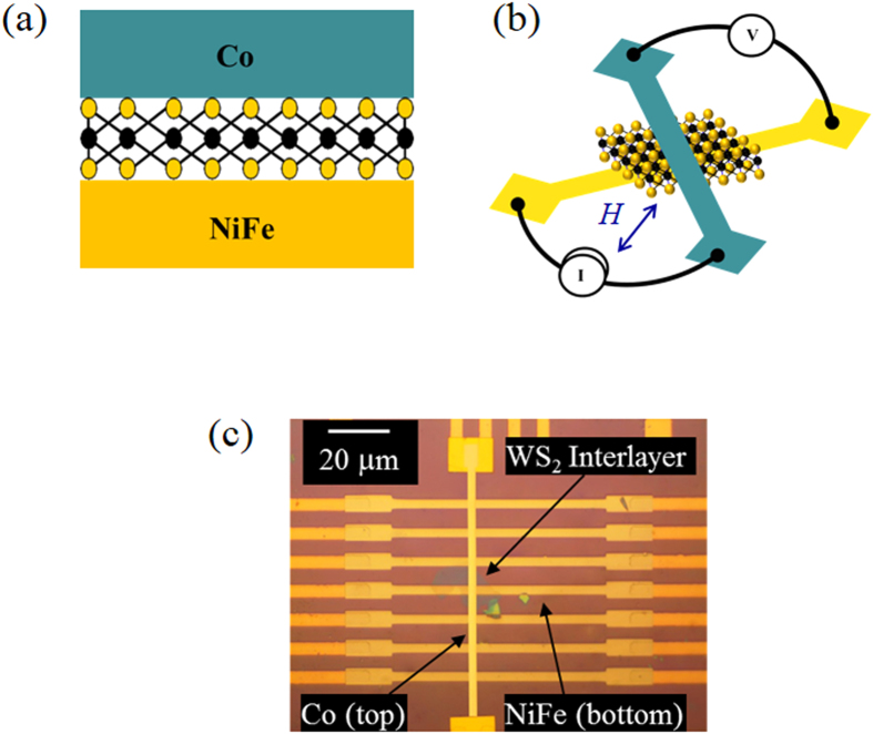
Figure 1(a) shows a schematic of WS2 spin valve consisting of top Co electrode, bottom NiFe electrode and a WS2 interlayer. The device structure and the measurement configuration are shown in Fig. 1(b). While current flows from Co to NiFe through WS2 interface, voltage is measured between Co and NiFe. The in-plane magnetic field (H) was applied at 45° to the direction of the ferromagnetic (FM) electrodes. Therefore the magnetization alignments can be made semi-parallel or semi-antiparallel by sweeping H. The optical micrograph of the complete device is portrayed in Fig. 1(c).
Figure 1.
(a) Schematic view of WS2 spin valve consisting of top Co electrode, bottom NiFe electrode and a WS2 interlayer. (b) The measurement configuration of spin valve device. Magnetic field (H) is applied in plane and at oblique angle to the ferromagnetic electrode axis. (c) Optical micrograph of the complete NiFe/WS2/Co device.
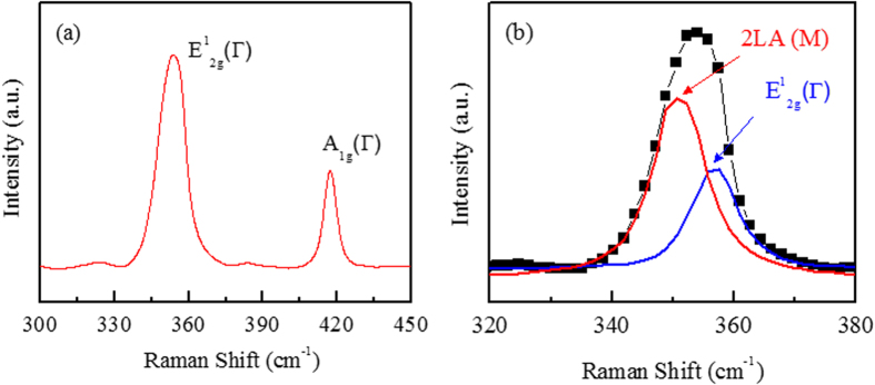
Figure 2(a) shows Raman spectrum measured for the WS2 film. Raman spectra of the SL-WS2, film show strong signals of in-plane  , out-of-plane
  , and vibration second-order 2LA(M) modes. The first-order
  and
and  optical modes were used to identify the 2D materials, such as MoS2, but the intensity of the 2LA(M) mode at 352 cm−1 was considerably higher for WS2. The Raman peak positions of
  and
and  for SL-WS2 are 355.2 and 417.7 cm−1 respectively. The frequency difference between Raman
  and
and  modes
modes  is about 62.5 cm−1, which indicates a single layer of the WS2 film11,22,23. However, the 2LA(M) mode was overlapped with the first-order
  mode at 355.2 cm−1, Lorentzian peaks fitting clarify the contribution of each peak as shown in Fig. 2(b)11.
Figure 2.
(a) Raman spectra (514 nm wavelength) of single layer WS2 film after transferred to the Si/SiO2 substrate. (b) Lorentzian peaks fitting to identify the positions 2LA(M) and first-order  mode.
mode.
Spin valve effect and current-voltage characteristics in WS2-interlayer junction
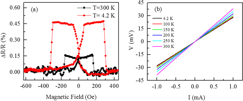
The spin valve effect was studied by examining the relative magnetoresistance ratio (MR), which is defined by MR = [RAP − RP]/RP. Here, RAP is the magnetic field dependent resistance and RP is the resistance corresponding to the parallel alignment of magnetizations. Figure 3 (a) shows MR signal of NiFe/SL-WS2/Co spin valve device. The value of MR shows bistable states where high (low) resistance appears in the antiparallel (parallel) magnetization configuration between Co and NiFe. The magnitude of MR value is observed of the order of 0.18% at 300 K and 0.47% at 4.2 K. We have further investigated the nature of NiFe/SL-WS2/Co junction by measuring current-voltage (I–V) characteristics. The I–V curves of the junctions at various temperatures range from 4.2 K to 300 K are shown in Fig. 3(b). The linear behavior of I–V curves indicate the ohmic characteristics of the junctions.
Figure 3.
(a) Magnetoresistance ratio of the NiFe/WS2/Co spin valve device as a function of magnetic field (H) at 4.2 K and 300 K. Magnetoresistance ratio is in the high (low) state for the antiparallel (parallel) magnetization configuration between NiFe and Co. (b) The current-voltage (I–V) characteristics of the NiFe/SL-WS2/Co junction at various temperatures range from 4.2 K to 300 K.
Temperature dependence of the spin valve effect
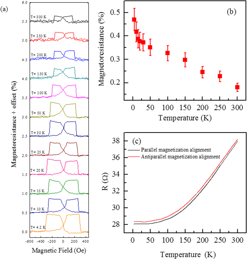
The WS2-interlayer spin valve device reveals a sequence of MR curves at various temperatures ranging from 300 K to 4.2 K as shown in Fig. 4(a). The magnitude of the spin valve signal having MR monotonically decreases as the temperature is increased. The decrease of MR at higher temperature can be attributed to many possible origins such as magnetic impurity scattering, surface states, and thermal smearing of the electron energy distribution in ferromagnetic24. The similar temperature dependence has been observed in magnetic tunnel junction25. The switching points of MR curves becomes broader at low temperature due to increasing switching fields of FM as thermal agitation is weakened. The trend of increment in the MR values as a function of temperature is shown in Fig. 4(b).
Figure 4.
(a) Magnetoresistance ratio (MR) as a function of magnetic field (H) for the WS2 spin valve at various temperatures. The spin valve signals are observed at all temperatures in the experiment. However, the magnitude of MR increases by reducing the temperature. (b) The variation in the MR values as a function of temperature. (c) The junction resistance WS2 spin valve as a function of temperature.
The resistance of WS2 interlayer junction in the parallel and antiparallel magnetization alignment is measured as a function of temperature. The junction resistance decreases monotonically as temperature is lowered as shown in Fig. 4(c). These observations suggest that the role of WS2 film as metallic interlayer instead of semiconducting nature. The theoretical evidence also suggests that the metallic nature of metal dichalcogenide films7. The distance between the ferromagnetic surface atoms and nearest S atoms is d = 2.1 Å. Therefore, the bonding between metal dichalcogenide film and ferromagnetic electrode permits a strong wave-function overlap between the Mo/W and ferromagnetic states. The junction shows metallic nature with the pristine gap of metal dichalcogenide film being absent leading to a large transmission. Because the Fermi level is pinned at the conduction band minimum and therefore it is also evinced that the projected densities of states on Mo/W atoms shows no energy gap.
Current bias dependence of the spin valve effect
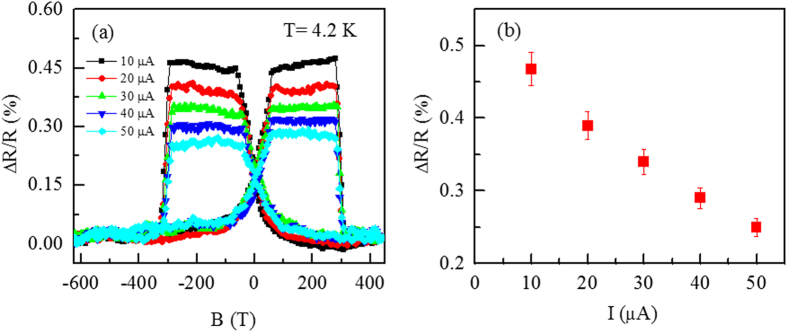
The magnetoresistance variation is examined by applying various bias current on the junction. Figure 5 (a) shows the spin valve effect at different bias currents from 10 μA to 50 μA. The results reveal that by increasing bias current the magnetoresistance is decreased. The trend of change in magnetoresistance as a function of bias current is shown in Fig. 5(b). The decrease of magnetoresistance by increasing bias current is attributed to the localized trap states in the interlayer26.
Figure 5.
(a) The magnetoresistance of spin valve as a function of magnetic field at different bias current values range from 10 μA to 50 μA. (b) The change in magnetoresistance for different bias current values.
Conclusions
In conclusion, we have demonstrated spin valve effect in single layer WS2 film as an intervened layer between NiFe and Co electrodes. Our results show that the spin valve effect of WS2 junction have relative magnetoresistance in spin valve effect increases from 0.18% at room temperature to 0.47% at 4.2 K. We observed that junction resistance decreases monotonically by reducing the temperature. These results revealed that semiconducting WS2 thin film works as a metallic conducting interlayer between NiFe and Co electrodes. The WS2 interlayer spin valve junction is expected to be an attractive candidate for future spintronic devices and may contribute to open new avenues for the industrial application.
Experimental Section
Material and device fabrication
The single layer WS2 film was obtained by mechanically exfoliating natural WS2 using adhesive tape and then the flake was transferred onto the pre-patterned Py electrodes on SiO2/Si substrate using wet transfer method. The single layer (SL) was initially identified by optical microscopy and then further confirmed by Raman spectroscopy. The device fabrication is categorized into three different parts; bottom Py film, WS2 film transfer, and top Co film. Before that the outer patterns were made on Si substrate with SiO2 thickness of 300 nm using photo-lithography and Cr/Au (5/30 nm) deposition. The bottom Py electrodes were initially patterned using e-beam lithography. A standard lift-off procedure was used to obtain the bottom electrode lines after evaporating Py with thickness of 55 nm. Then a single layer WS2 was transferred on top of bottom Py electrodes. In the subsequent process top Co electrode with thickness of 75 nm was patterned by using e-beam lithography and lift-off process. The width of both top and bottom electrodes were 3 μm.
Device characterization and measurement setup
Renishaw Raman micro-spectrometer was use to characterize the WS2 samples. The laser wavelength of the spectrometer was 514 nm, and the power was kept below 1.0 mW to avoid laser-induced heating. The transport measurements for WS2 based spin valve devices were performed using ac lock-in technique. The bias currents was kept 10 μA for temperature dependent spin transport measurements and further increased up to 50 μA to study the effect of bias dependence. The devices were cooled by liquid helium for low temperature measurements and the temperature was modulated by Lake Shore 331 temperature controller.
Additional Information
How to cite this article: Iqbal, M. Z. et al. Room temperature spin valve effect in NiFe/WS2/Co junctions. Sci. Rep. 6, 21038; doi: 10.1038/srep21038 (2016).
Acknowledgments
The authors would like to extend their sincere appreciation to the Deanship of Scientific Research at King Saud University for funding this research group no. RG1435-004.
Footnotes
Author Contributions M.Z.I. conceived and designed the study. M.Z.I. performed the experiments. M.Z.I. wrote the manuscript. M.W.I., S.S., M.F. K. and S.M. R. helped in device fabrication and characerization. All authors contributed to discussion and reviewed the manuscript.
References
- Iqbal M. Z. et al. Spin valve effect of NiFe/graphene/NiFe junctions. Nano Res. 6, 373–380 (2013). [Google Scholar]
- Iqbal Z. M., Iqbal W. M., Jin X., Hwang C. & Eom J. Interlayer dependent polarity of magnetoresistance in graphene spin valves. J. Mater. Chem. C 3, 298–302 (2015). [Google Scholar]
- Meng J., Chen J.-J., Yan Y., Yu D.-P. & Liao Z.-M. Vertical graphene spin valve with Ohmic contacts. Nanoscale 5, 8894–8898 (2013). [DOI] [PubMed] [Google Scholar]
- Chen J.-J. et al. Layer-by-layer assembly of vertically conducting graphene devices. Nat. Commun. 4, 1921 (2013). [DOI] [PubMed] [Google Scholar]
- Cobas E., Friedman A. L., van’t Erve O. M., Robinson J. T. & Jonker B. T. Graphene as a tunnel barrier: graphene-based magnetic tunnel junctions. Nano Lett. 12, 3000–3004 (2012). [DOI] [PubMed] [Google Scholar]
- Dankert A., Kamalakar M. V., Wajid A., Patel R. & Dash S. P. Tunnel magnetoresistance with atomically thin two-dimensional hexagonal boron nitride barriers. Nano Res. 8, 1357–1364 (2014). [Google Scholar]
- Wang W. et al. Spin-valve Effect in NiFe/MoS2/NiFe Junctions. Nano Lett. 15, 5261–5267 (2015). [DOI] [PubMed] [Google Scholar]
- Li F., Li T. & Guo X. Vertical Graphene Spin Valves Based on La2/3Sr1/3MnO3 Electrodes. ACS Appl. Mater. Interfaces 6, 1187–1192 (2014). [DOI] [PubMed] [Google Scholar]
- Entani S., Naramoto H. & Sakai S. Magnetotransport properties of a few-layer graphene-ferromagnetic metal junctions in vertical spin valve devices. J. Appl. Phys. 117, 17A334 (2015). [Google Scholar]
- Iqbal M. W. et al. High-mobility and air-stable single-layer WS2 field-effect transistors sandwiched between chemical vapor deposition-grown hexagonal BN films. Sci. Rep. 5, 10699 (2015). [DOI] [PMC free article] [PubMed] [Google Scholar]
- Iqbal M. W. et al. Deep-ultraviolet-light-driven reversible doping of WS2 field-effect transistors. Nanoscale 7, 747–757 (2015). [DOI] [PubMed] [Google Scholar]
- Khan M. F. et al. Photocurrent response of MoS2 field-effect transistor by deep ultraviolet light in atmospheric and N2 gas environments. ACS Appl. Mater. Interfaces 6, 21645–21651 (2014). [DOI] [PubMed] [Google Scholar]
- Braga D., Gutiérrez Lezama I., Berger H. & Morpurgo A. F. Quantitative determination of the band gap of WS2 with ambipolar ionic liquid-gated transistors. Nano Lett. 12, 5218–5223 (2012). [DOI] [PubMed] [Google Scholar]
- Moodera J. S. & Mathon G. Spin polarized tunneling in ferromagnetic junctions. J. Magn. Magn. Mater. 200, 248–273 (1999). [Google Scholar]
- Suezawa Y. & Gondō Y. Spin-polarized electrons and magnetoresistance in ferromagnetic tunnel junctions and multilayers. J. Magn. Magn. Mater. 126, 524–526 (1993). [Google Scholar]
- Wei H., Qin Q., Ma M., Sharif R. & Han X. 80% tunneling magnetoresistance at room temperature for thin Al-O barrier magnetic tunnel junction with CoFeB as free and reference layers. J. Appl. Phys. 101, 09B501 (2007). [Google Scholar]
- Ikeda S. et al. Tunnel magnetoresistance of 604% at 300 K by suppression of Ta diffusion in CoFeB/MgO/CoFeB pseudo-spin-valves annealed at high temperature. Appl. Phys. Lett. 93, 2508 (2008). [Google Scholar]
- Butler W., Zhang X.-G., Schulthess T. & MacLaren J. Spin-dependent tunneling conductance of Fe| MgO| Fe sandwiches. Phys. Rev. B 63, 054416 (2001). [Google Scholar]
- Ikeda S. et al. A perpendicular-anisotropy CoFeB–MgO magnetic tunnel junction. Nat. Mater. 9, 721–724 (2010). [DOI] [PubMed] [Google Scholar]
- Parkin S. S. et al. Giant tunnelling magnetoresistance at room temperature with MgO (100) tunnel barriers. Nat. Mater. 3, 862–867 (2004). [DOI] [PubMed] [Google Scholar]
- Yuasa S., Nagahama T., Fukushima A., Suzuki Y. & Ando K. Giant room-temperature magnetoresistance in single-crystal Fe/MgO/Fe magnetic tunnel junctions. Nat. Mater. 3, 868–871 (2004). [DOI] [PubMed] [Google Scholar]
- Berkdemir A. et al. Identification of individual and few layers of WS2 using Raman Spectroscopy. Sci. Rep. 3, 1755 (2013). [Google Scholar]
- Zeng H. et al. Optical signature of symmetry variations and spin-valley coupling in atomically thin tungsten dichalcogenides. Sci. Rep. 3, 1608 (2013). [DOI] [PMC free article] [PubMed] [Google Scholar]
- Akerman J. J., Roshchin I. V., Slaughter J. M., Dave R. W. & Schuller I. K. Origin of temperature dependence in tunneling magnetoresistance. Europhys. Lett. 63, 104–110 (2003). [Google Scholar]
- Shang C. H., Nowak J., Jansen R. & Moodera J. S. Temperature dependence of magnetoresistance and surface magnetization in ferromagnetic tunnel junctions. Phys. Rev. B 58, R2917–R2920 (1998). [Google Scholar]
- Tsymbal E. Y., Mryasov O. N. & LeClair P. R. Spin-dependent tunnelling in magnetic tunnel junctions. J. Phys.: Condens. Matter 15, R109 (2003). [Google Scholar]


