Abstract
A novel vertical 3D RRAM structure with greatly improved reliability behavior is proposed and experimentally demonstrated through basically compatible process featuring self-localized switching region by sidewall electrode oxidation. Compared with the conventional structure, due to the effective confinement of the switching region, the newly-proposed structure shows about two orders higher endurance (>108 without verification operation) and better retention (>180h@150 °C), as well as high uniformity. Corresponding model is put forward, on the base of which thorough theoretical analysis and calculations are conducted as well, demonstrating that, resulting from the physically-isolated switching from neighboring cells, the proposed structure exhibits dramatically improved reliability due to effective suppression of thermal effects and oxygen vacancies diffusion interference, indicating that this novel structure is very promising for future high density 3D RRAM application.
Flash is the mainstream of non-volatile memory (NVM), which is widely used in the field of embedded system and applied electronics. However, as the integration density continues rising, flash is reaching the physical limitation due to reliability issues as well as process cost. Thus various emerging memories with new storage mechanisms were put forward as candidates for flash replacement, such as ferroelectric random access memory (FeRAM), magnetic random access memory (MRAM), phase change random access memory (PRAM), resistive random access memory(RRAM) and so on1,2,3,4,5,6. Among them, RRAM attracts arising attentions due to its advantages of simple structure, excellent performance and outstanding scaling capability6,7,8. Recently, RRAM has been officially listed in International Technology Roadmap for Semiconductors (ITRS) as one of the most promising emerging memories in future9.
Resistive switching occurs in a wide range of materials among which the binary transition metal oxides (TMO) facilitate the simple fabrication process and stable structure, thus gained extensive attention. A large variety of candidate metal-oxide materials have been demonstrated for RRAM technology, such as TaOx10,11,12, HfOx13,14, TiOx15, AlOx16, CuOx17, and so on. Among them, TaOx -based RRAM has shown superior merits such as low operation voltage18, fast switching speed19, high thermal stability20, distinctive retention capability21,22, excellent uniformity23,24, as well as the process compatibility25, especially, the most prominent feature of TaOx -based RRAM is the extremely high endurance due to the simple thermodynamic equilibrium phases of Ta-O systems26,27,28,29, which paves the way for reliable storage application.
As mentioned above, in order to satisfy the exponentially grown needs for big-data storage, the integration density of storage system is continuously enlarging while the size of storage cell is continuously scaling. Although a high-density 16 Gb RRAM with 27 nm Technology has been recently reported30, the further shrinking of 2D RRAM size, especially in sub-10 nm era, strongly relies on complex processes and advanced lithography technology, facing the cost and fabrication challenges31, which hinders RRAM as replacement of NAND flash memory for low-cost mass storage. Therefore, several 3D RRAM structures have been presented aiming to competing with 3D NAND technology in the future32,33,34. Wherein compared with horizontal 3D structure that simply stacking 2D RRAM cells layer by layer which inevitably increasing cost of patterning35, vertical 3D RRAM, especially vertical 3D TMO-based RRAM (TMO VRRAM) has been considered as a more promising candidate for future ultra-high density non-volatile memory applications in terms of the bit-cost scalability, high switching speed and low power consumption36,37.
Nowadays the researches on 3D RRAM mainly focus on the scalability of both vertical and horizontal dimensions to increase the storage capability, and sub-nm sidewall electrode are demonstrated in different researches38,39. However, the accompanying reliability problems demand much more consideration, especially for the additional dimension in 3D RRAM compared with 2D structure. To be specific, the reported TMO VRRAMs based on transition metal oxides so far, usually have a whole continuous metal oxide layer formed along the sidewall of the hole etched through multiple stacks36,37,38,39, which may cause reliability degradation originated from oxygen vacancies diffusion along this continuous oxide layer, particularly when stacks are scaled to extremely small dimensions. One typical example is that disturbance may occur to the vertical adjacent unselected cell when operating the selected cell, which may even cause function disability40.
It is widely accepted that the resistive switching of RRAM is strongly correlated to the defects modification in switching oxide; specifically, the movement of oxygen ions plays a decisive role in characteristics of TMO-based RRAM devices1,2,3. Therefore, unwanted diffusions of oxygen ions in switching layer will have serious impacts on the reliability and performance, or even functions of RRAM41,42. In this regard, effective isolation of vertical adjacent cells is critical to cut off unwanted diffusion paths of oxygen ions, and then restrain the performance degradation. In 2D RRAM, several solutions are put forward to reduce the unwanted oxygen vacancies lateral diffusion, including cutting off the continuous metal oxide layer by etching and introducing encapsulated cell structure by patterning20,43,44,45. However, these approaches are not practical for 3D VRRAMs for the reason that the continuous metal oxide layer along the sidewall cannot be easily patterned and selectively etched.
In this work, a novel 3D vertical RRAM structure was proposed and successfully demonstrated by two-layer stacked 3D TaOx RRAM. The unique difference is that in the proposed structure, thermal oxidation is adopted to form the self-localized switching cells (TaOx) which is only located on the separated sidewall electrode (Ta) layer, naturally isolated by the undisturbed isolation layer. While in conventional structure, atomic layer deposition (ALD) or physical vapor deposition (PVD) may unavoidably form the whole continuous resistive switching film, which also exists besides the isolation layer. Therefore, the simply change of the switching layer formation process by sidewall electrode oxidation (SEO) effectively cuts off the vertical adjacent resistive switching layers without increasing process complexity or consuming additional area, demonstrating dramatic reliability improvements and scaling capability of the proposed structure.
Results and Discussion
A. Sidewall electrode oxidation optimization
According to the previous reports46,47,48, the properties of tantalum oxide formed by Ta oxidation mainly depend on oxidation process conditions, especially on oxidation temperature and time: below 400 °C, most of the oxygen is dissolved in the tantalum lattice (which is called the solution of interstitial oxygen)46, while above 400 °C, the oxidation rate becomes faster as the annealing temperature rises47; additionally, after the complete oxidation, the thickness of the oxidized part would double48.
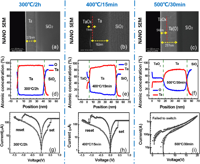
As in our device, since the switching material is formed through oxidation of Ta sidewall electrode, Ta oxidation condition and optimization are critical to the proposed structure. Therefore, three annealing conditions (300 °C/2 h, 400 °C/15 min, 500 °C/30 min) were investigated with comprehensive consideration of temperature and time to fabricate 2D RRAM devices with simply metal-insulator-metal (MIM) structure (Ta/TaOx/Pt) (See Oxidation Optimization in Methods section), allowing for both the component analysis as well as corresponding electrical measurements (as shown in Fig. 1).
Figure 1.
SEM cross-section images (Top-(a–c)); AES profile (Middle-(d–f)); and corresponding device switching characteristics (Bottom-(g–i)) of sidewall electrode oxidation experiments under different annealing conditions: annealing 2 h/300 °C (Left-(a,d,g)); annealing 15 min/400 °C (Middle-(b,e,h)); annealing 30 min/500 °C (Right-(c,f,i)). The thickness of oxidized TaOx layers increase with elevated temperature.
The combination of cross-sectional profiles provided by scanning electron microscope (SEM) images (Fig. 1(a–c)) and oxygen distributions along depth direction provided by auger electron spectroscopy (AES) (Fig. 1(d–f)) clearly show the different composition distributions in three annealing conditions. Among which, 400 °C/15 min annealing is enough to form 11 nm TaOx film with proper oxygen concentration gradient, demonstrating that the novel critical process of this novel structure meets the temperature requirement of CMOS back-end process. In addition, according to the DC measurement displayed in Fig. 1 (g–i), device annealed under 400 °C/15 min condition shows best switching characteristics. In comparison, 500 °C/30 min annealing devices cannot be switched due to the 94 nm thick oxide layer, and in case of 300 °C/2 h annealing samples, although there are some lucky devices can also be switched (on/off ratio smaller than 400 °C/15 min ones), their oxide thickness can hardly be detected (as depicted in Fig. 1(a,d)), indicating the risk of reproducibility and yield.
B. Novel 3D vertical RRAM fabrication
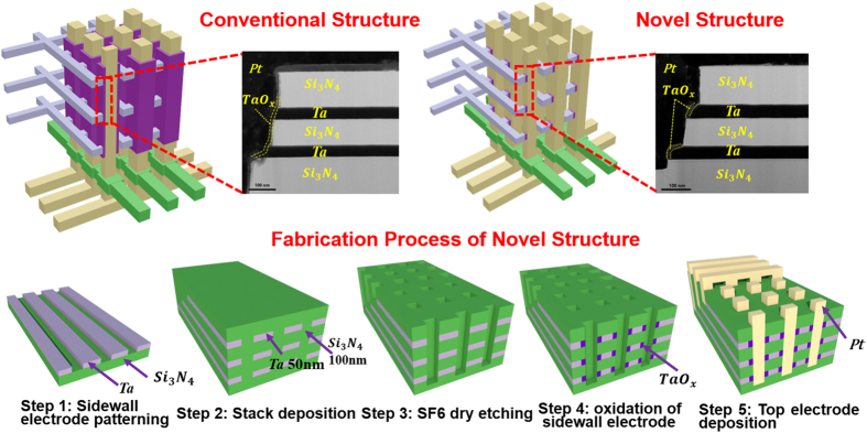
By utilizing the above optimized condition, the novel 3D VRRAM with cells in two vertical stacked layers is experimentally demonstrated based on Ta sidewall electrode oxidation, adopting 400 °C/15 min oxidation condition. Meanwhile, devices with conventional 3D structure are also fabricated as a comparison (See Device Fabrication in Methods section). The schematic view of both structures and the detailed fabrication processes of the proposed novel 3D RRAM cell are illustrated in Fig. 2. The core distinction of the fabrication processes of both structures lies in that, instead of PVD or ALD to form a continuous switching layer in conventional structure, partially oxidation of the isolated sidewall electrodes can naturally form the self-confined switching areas on the edge of sidewall electrodes in the novel 3D structure. The transmission electron microscope (TEM) and energy dispersive x-ray spectroscopy (EDX) characterizations confirm the differences as shown in Figs 3 and 4.
Figure 2. (Top) 3D vertical RRAM array architecture of conventional structure with continuous oxide resistive switching layer, and novel structure with self-localized resistive switching region formed around Ta sidewall electrode.
TEM images of enlarged view of RRAM cells in both structures demonstrate the differences. (Bottom) Fabrication process of the proposed novel 3D vertical RRAM structure.
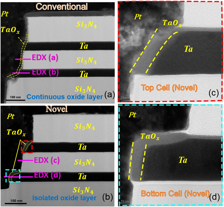
Figure 3.
TEM images of (a) conventional structure; (b) proposed novel structure; (c) top cell in the proposed novel structure; (d) bottom cell in the proposed novel structure. TEM images clearly show that the switching layers of top cell and bottom cell are a consecutive TaOx film in conventional structure while the switching regions are isolated by Si3N4 layer and confined to the Ta sidewall electrodes. The proposed SEO structure is well demonstrated here.
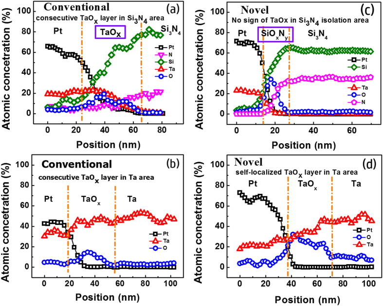
Figure 4.
(Left) Horizontal EDX line scans with corresponding elements profiles labeled as (a,b) in Fig. 3(a); (Right) Horizontal EDX line scans with corresponding elements profiles labeled as (c,d) in Fig. 3(b). EDX analysis of elements profile further confirms the switching region in the proposed SEO structure is totally isolated by Si3N4 layer.
TEM images display that the spontaneously confined TaOx switching regions only exist around the sidewall electrodes after annealing in the proposed novel structure (Fig. 3(a)), while a consecutive TaOx switching layer deposited by sputtering covers on the whole sidewall of the hole-region in conventional structure (Fig. 3(b)). To further carefully compare the elements profile differences between both structures, EDX component analysis are conducted on the isolation layer and sidewall electrode region near sidewall of the hole in both structures. Shown by the Fig. 4(a,b), TaOx can be seen only in the resistive cell region in the novel structure, and no TaOx in the counterpart of the isolation layer, while TaOx exists in both cell and isolation layers in conventional structure (Fig. 4(c,d)). Additionally, in conventional structure cell region shown by Fig. 4(a), it is observed that element N is detected in the TaOx region besides the isolation Si3N4 layers, indicating that a conducting TaN phase may be formed by reaction between Ta2O5 and Si3N4, raising the risk of short-circuiting the vertical adjacent cells. By contrast, the cells in novel structure are cut off completely without the similar concerns, further demonstrating the improvements.
It is worth noting that the concentration gradient in novel 3D structure is similar to that of the optimization experiment in Fig. 1, which validates that our self-confined 3D structure will not affect the oxidation process to form TaOx with uniform quality which can ensure the resistive switching properties. In addition, the enlarged TEM images (Fig. 3c,d) indicate that switching layer thicknesses of top and bottom cells are also similar to the 2D cell with the same optimized annealing condition, which further indicates the stability and uniformity of the critical oxidation process. This feature is essential for RRAMs to maintain highly uniform performance in 3D era with scaled dimensions. For instance, as the increase of stacking layers and the decrease of hole dimensions, the conformality of TMO switching layer deposition (PVD or ALD) process would inevitably get deteriorated due to the limitation of conventional etching and deposition processes, leading to the severe variations of deposited switching layer thickness and consequently resulting in electrical performance dispersions in conventional 3D VRRAM devices. However, in case of the proposed structure, the thickness of switching TMO layer is mainly determined by partially oxidation of sidewall electrodes, which is not sensitive to the scaled dimension of 3D structure, facilitating the uniform formation of switching cells and accordingly the good device-to-device uniformity control.
C. Switching characteristics
Electrical characterizations were performed on Agilent B1500A semiconductor characterization system. During the measurements, the voltage is applied on Ta sidewall electrode, while keeping Pt top electrode grounded all the time.
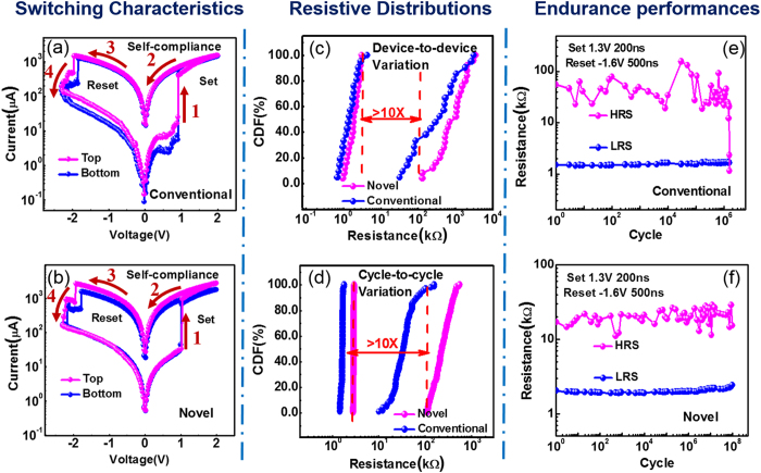
The typical switching characteristics of novel structure and conventional structure are displayed in Fig. 5(a,b), respectively. The resistance switching occurs along direction of the arrows shown in the figures, with set voltage about 1V and reset voltage about 2V in both structures, which meets the requirement of integration. Meanwhile, the very similar performances demonstrate that the switching layer formed by optimized oxidation process in novel structure exhibits the comparable switching characteristics with the sputtering switching layer in conventional structure, which further confirms the TEM and EDX results in Figs 3 and 4. In addition, the identical characteristics of the up- and bottom- cell in the proposed structure complementally verifies the process uniformity of sidewall electrode oxidation (SEO), corresponding to the same thicknesses in both layer shown in Figs 3 and 4. Furthermore, switching window >10X was obtained without requiring current compliance in reset operation, which is beneficial to simplify the peripheral circuit design. The excellent self-compliance and controllable reset process are due to the gradient profile of oxygen concentration in TaOx corresponding to the SEO process.
Figure 5.
(Switching Characteristics) Typical I-V curves from randomly chosen adjacent cells in both conventional structure (a) and proposed SEO structure (b). The devices show not only excellent bipolar switching characteristics but also nearly identical initial switching curves. (Resistive Distributions) Resistive distributions in conventional structure and proposed SEO structure. (c) device-to-device variability obtained from 30 randomly selected devices; (d) cycle-to-cycle variability obtained from 107 consecutive pulse operation cycles. HRS/LRS ratio >10X is obtained in proposed SEO structure. (Endurance performances) Endurance characteristics of conventional structure and proposed SEO structure. Pulse operation configuration: set 1.3 V/200 ns; reset −1.6 V/500 ns. ~108 cycles was obtained without verification and any noticeable degradation in proposed SEO structure. Conventional structure degrades after ~106 cycles.
Since that the distributions of resistance are critical parameters for memory array performance and also key issues for 3D RRAM array integration, 30 randomly selected devices were measured to obtain the cumulative probability of both structures, as well, cycle-to-cycle variability was obtained from 107 consecutive pulse operation cycles in one randomly selected device of both structures, respectively. Compared with conventional structure, remarkable improvements of both device-to-device (Fig. 5(c)) and cycle-to-cycle (Fig. 5(d)) uniformity of HRS are achieved in the novel structure. As mentioned above, the SEO process helps to form uniform oxide films in different layers, thus improving the device-to-device uniformity. At the same time, the enhanced cycle-to-cycle uniformity is mainly benefited from the confined switching region which can effectively suppress the diffusion of oxygen vacancies (VOs) and consequently improving the stability of the conductive filaments (CFs) morphology.
D. Reliability behaviors
The comparison of reliability performances (endurance and retention) was also experimentally performed in detail. During pulse measurements, the proper pulse programming conditions are optimized as: 1.3 V/200 ns for set operation and −1.6 V/500 ns for reset operation without any verification operation. Endurance as high as ~108 cycles was obtained without any noticeable degradation in the proposed cell structure (Fig. 5(e)). In contrast, (Fig. 5(f)) shows that the HRS of the conventional cell degraded at only ~106 cycles under the same test configuration. The marvelous improvement of endurance capability of the novel 3D structure is attributed to the more confined oxygen distribution of physically isolated resistive cells due to SEO process. To be specific, in the novel structure, benefited from the good isolation, oxygen vacancies (VOs) involved in the formation or rupture of CFs in the cell region can be well maintained as the cycling times increasing, thus significantly mitigating the endurance degradation.
As for the non-volatile memory (NVM), retention property determines the time limit for data storage, which is the critical reliability parameter. In the case of RRAM, the degradation of low resistive state (LRS) is more serious, since that the CFs evolution in LRS is directly related to the VOs diffusions under the action of both concentration gradient and thermal effect. Especially in small dimensions, the trade-off of retention and low operation current gets more obvious41, for the reason that the CFs are more vulnerable in the low current region and small sizes. This degradation will be more serious in 3D structures as the heat accumulation is more obvious due to the heat dissipation problems of the complex multi-layer structures. In this paper, in order to carefully investigate the influence of 3D structures on the retention performances as well as the VOs diffusion behavior, devices of four different resistance states (LRS-1, LRS-2, LRS-3 & HRS) of both structures were baked at 150 oC. As shown in Fig. 6, both low resistive state (LRS) and high resistive state (HRS) of conventional devices exhibit distinct drift to higher resistance states. And notably, the aggravation of retention degradation with increased LRS in conventional devices well demonstrates the trade-off between retention capability and low current operation in conventional 3D structure41. However, only slight changes in all the four resistive states were observed in the novel structure devices (Fig. 6) even after the 180 h baking, indicating the superior retention feature of the proposed structure. Furthermore, the proposed structure, with good stability of relative high resistance in LRS, also demonstrates great potential for low power application.
Figure 6. Retention behavior of four different resistive states (LRS_1 (103 ohm), LRS_2 (3*104 ohm), LRS_3 (106 ohm), HRS (108 ohm)) at 150 °C for conventional structure and proposed SEO structure.
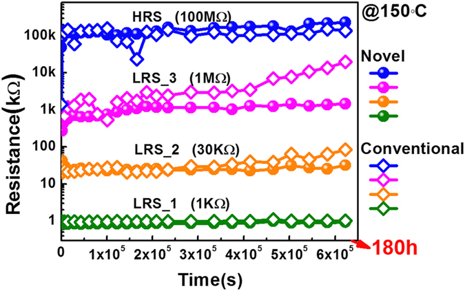
For conventional structure, resistance state shows distinct drift to higher resistance state. For proposed SEO structure, each resistance state can maintain almost unchanged >180 h@150 °C.
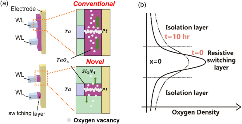
We believe that the significant reliability improvements of the proposed sidewall electrode oxidation (SEO) cell are due to the automatic formation of self-confined switching area which can significantly inhibit the degradation caused by the combination of oxygen vacancies diffusion and thermal effect during switching process. Additionally, adoption of Si3N4 dielectric layers, which acts as powerful oxygen-blocking layers and heat sinks43,44,45, further prevents the unwanted diffusions of oxygen vacancies. It is widely accepted that CF consisting of VOs in TMO RRAM device has higher VO concentration in the center of CF and the redistribution of VOs driving by concentration gradient and thermal effect will give critical impacts on resistance drift of LRS and consequently retention characteristics of RRAM devices21,22. Figure 7(a) illustrates the schematic diagram of oxygen vacancies diffusions inside the proposed SEO cell and the conventional cell. A thermal diffusion model was proposed to gain insightful understanding of the reliability issues (Fig. 7(b)), based on which distribution of VOs density in the resistive cell region versus time can be calculated.
Figure 7.
Schematic diagram of (a) Oxygen vacancies diffusion inside the conventional structure and the proposed SEO structure; (b) thermal diffusion model of the time dependent oxygen vacancies density distribution.
Corresponding to Fig. 7(b), the vertical direction in 3D structure is set as X axis to calculate the diffusion of VOs between resistive cell and the adjacent isolation layer or resistive film in both structures. The processes of VOs concentration varying with time in the resistive cell regions can be described by the following equations21,22:
VOs concentration
 |
In which, c(x, t) is the time-varying VOs concentration along the cell region, QT is the total quantity of oxygen vacancies per unit area, D is the diffusion coefficient with the expressions as follows:
Diffusion coefficient
 |
Intrinsic diffusion coefficient
 |
where Ea is the activation energy (1.16 ev for TaOx21 and >4.7 eV49 for Si3N4), k is the Boltzmann constant (1.38 × 10⁻²³ J/K), q is the electron charge (1.6 × 10⁻¹⁹C), λ is the lattice constant in isolation layer (0.76 for TaOx and 0.79 for Si3N4), f is the oscillation frequency of phonon (~1013).
Furthermore, since cell resistance is mainly related to the oxygen vacancies distribution, resistance change versus time due to VOs diffusion can be derived from VOs density evolution versus time. As shown in Fig. 8(a), by characterizing the temperature dependence of LRS for both structures, the conduction mechanism is demonstrated as variable range hopping21,50, with the relationship between conductivity and VOs density as expression (4):
Figure 8. Calculated LRS_2 (fittings of other resistances are not shown here) degradation from the proposed model of the conventional structure and the proposed SEO structure at 150 °C fits well with the experimental data.
With the standard of 20% resistance change, the proposed SEO structure shows highly improved retention behavior in comparison with the conventional structure.
 |
in which, α is calculated as −7 @150 oC corresponding to the measurements, and β is  based on the demonstrated variable range hopping conduction mechanism. Accordingly, the change of resistance can be calculated based on the model mentioned as Fig. 7, which fits well with the measured retention data (LRS_2) obtained from both novel and conventional cells (Fig. 8(b,c)), which proves the conclusion that the thermal diffusions of VOs is well suppressed in our novel structure even under high temperature and hence dramatically improves the cell retention reliability.
Conclusion
In this study, remarkable improvements of reliability (endurance: ~108 and retention: ~180 h@150 oC) are achieved by introducing a novel structure of TaOx-based 3D vertical RRAM with self-localized switching layer. The newly proposed 3D structure demonstrates excellent self-compliance performance and outstanding cycle-to-cycle and device-to-device uniformity as well. The proposed thermal diffusion model well explains the reliability improvements, and analysis of the experimental data indicate that the spontaneous formation of the self-confined switching region by proposed SEO can effectively inhibit the diffusion of oxygen vacancies as well as suppressing the thermal impacts, indicating that the proposed 3D structure has great potential for ultra-high density non-volatile memory.
Methods
Oxidation Optimization
The 2D RRAM devices for optimization experiments are fabricated by the following processes: At first, 100 nm SiO2 was deposited on Si wafers by plasma enhanced chemical vapor deposition (PECVD) as isolation layer, and then 170 nm Ta was deposited by PVD and patterned as the bottom electrode (BE). Next, the three samples are annealed in different conditions, i.e. 300 oC/2 h, 400 oC/15 min, 500 oC/30 min. Finally 300 nm PVD Pt was deposited as top electrode (TE).
Device Fabrication
Detailed fabrication processes of the proposed novel 3D RRAM cell as well as the conventional structure are illustrated as follows: Firstly, 100 nm Si3N4 was deposited on Si wafers by PECVD as isolation layer, and Ta sidewall electrode (50 nm) was deposited by DC sputtering and patterned by lift-off process respectively as one layer of sidewall electrode. And then, to form a 3D stack, by alternate deposition of Si3N4/Ta, stacked multilayer thin films were formed, and formation of the via holes was realized by photolithography and dry etching. The above process steps are the same for both structures. Subsequently, in case of the proposed structure, the self-confined switching area was formed by partially oxidizing the Ta sidewall electrode through annealing in oxygen ambient (400 oC/15 min). For a comparison, in this step, a consecutive 15 nm TaOx switching layer was deposited by RF sputtering (Ar: O = 12:8, 500 W) in case of the conventional cell. Finally, 300 nm Pt pillar electrode was formed by DC sputtering and lift-off process for both structure to complete the fabrication.
Additional Information
How to cite this article: Yu, M. et al. Novel Vertical 3D Structure of TaOx-based RRAM with Self-localized Switching Region by Sidewall Electrode Oxidation. Sci. Rep. 6, 21020; doi: 10.1038/srep21020 (2016).
Acknowledgments
This work is supported in part by National Natural Science Foundation of China (No. 61421005, No.61376087, and No. 61574007), National High Technology Research and Development Program of China (No. 2011AA010401 and No. 2011AA010402), and National Basic Research Program of China (No. 2011CBA00601).
Footnotes
Author Contributions M.X.Y., Y.M.C. and R.H. conceived the idea and designed this work. M.X.Y. fabricated the devices and performed most of the measurements. Y.C.F. and Y.F.L. preformed the calculations. Z.W.W. and Z.X.Z. contributed to the figure processing. Y.C.F., Z.Z.Y., Y.P., J.T. and X.Y. contributed to the measurements. All the authors discussed and analyzed the results. M.X.Y. and Y.M.C. wrote the manuscript. Y.M.C., M.L. and R.H. supervised this work.
References
- Meena J.-S., Sze S.-M., Chand U. & Tseng T.-Y. Overview of emerging nonvolatile memory technologies. Nanoscale Res. Lett. 9, 526 (2014). [DOI] [PMC free article] [PubMed] [Google Scholar]
- Burr G. W. et al. Overview of candidate device technologies for storage-class memory. IBM J. Res. Dev. 52, 449–464 (2008). [Google Scholar]
- Bez R. & Pirovano A. Non-volatile memory technologies: emerging concepts and new materials. Mater. Sci. Semicond. Process. 7, 349–355 (2004). [Google Scholar]
- Chen F. T. et al. Resistance switching for RRAM applications. Sci. China Inf. Sci. 54, 1073–1086 (2011). [Google Scholar]
- Duan S., Hu X., Wang L. & Li C. Analog memristive memory with applications in audio signal processing. Sci. China Inf. Sci. 57, 042406 (2014). [Google Scholar]
- Waser R., Dittmann R., Staikov G. & Szot K. Redox-based resistive switching memories nanoionic mechanisms, prospects, and challenges. Adv. Mater. 21, 2632–2663 (2009). [DOI] [PubMed] [Google Scholar]
- Yang J. J., Strukov D. B. & Stewart D. R. Memristive devices for computing. Nat. Nanotechnol. 8, 13–24 (2013). [DOI] [PubMed] [Google Scholar]
- Wong H.-S. P. et al. Metal–oxide RRAM. Proc. IEEE 100, 1951–1970 (2012). [Google Scholar]
- International Technology Roadmap for Semiconductors: 2013 Edition - Emerging Research Devices. (2013) Available at: http://www.itrs.net/home.html. (Accessed: 8th November 2015).
- Kim S. et al. Physical electro-thermal model of resistive switching in bi-layered resistance-change memory. Sci. Rep. 3, 1680 (2013). [DOI] [PMC free article] [PubMed] [Google Scholar]
- Yang M.-K., Ju H., Kim G.-H., Lee J.-K. & Ryu H.-C. Direct evidence on Ta-metal phases igniting resistive switching in TaOx thin film. Sci. Rep. 5, 14053 (2015). [DOI] [PMC free article] [PubMed] [Google Scholar]
- Wang Y.-F., Lin Y.-C., Wang I.-T., Lin T.-P. & Hou T.-H. Characterization and modeling of nonfilamentary Ta/TaOx/TiO2/Ti analog synaptic device. Sci. Rep. 5, 10150 (2015). [DOI] [PMC free article] [PubMed] [Google Scholar]
- Lv H. et al. Evolution of conductive filament and its impact on reliability issues in oxide-electrolyte based resistive random access memory. Sci. Rep. 5, 7764 (2015). [DOI] [PMC free article] [PubMed] [Google Scholar]
- Yu S., Guan X. & Wong H.-S. P. Conduction mechanism of TiN/HfOx/Pt resistive switching memory: A trap-assisted-tunneling model. Appl. Phys. Lett. 99, 063507 (2011). [Google Scholar]
- Kim K. M., Park T. H. & Hwang C. S. Dual conical conducting filament model in resistance switching TiO2 thin films. Sci. Rep. 5, 7844 (2015). [DOI] [PMC free article] [PubMed] [Google Scholar]
- Sugiyama I. et al. Spatially-resolved mapping of history-dependent coupled electrochemical and electronical behaviors of electroresistive NiO. Sci. Rep. 4, 6725 (2014). [DOI] [PMC free article] [PubMed] [Google Scholar]
- Zhou P. et al. Role of TaON interface for CuxO resistive switching memory based on a combined model Role of TaON interface for CuxO resistive switching memory based. Appl. Phys. Lett. 94, 053510, (2009). [Google Scholar]
- Ueki M. et al. Low-power embedded ReRAM technology for IoT applications. In Tech. Dig. VLSI Symp. Technol. 2015 T108–T109; 10.1109/VLSIC.2015.7231367 (2015). [DOI] [Google Scholar]
- Torrezan A. C., Strachan J. P., Medeiros-Ribeiro G. & Williams R. S. Sub-nanosecond switching of a tantalum oxide memristor. Nanotechnology 22, 485203 (2011). [DOI] [PubMed] [Google Scholar]
- Hayakawa Y. et al. Highly reliable TaOx ReRAM with centralized filament for 28-nm embedded application. In Tech. Dig. VLSI Symp. Technol. 2015 T14–T15; 10.1109/VLSIT.2015.7223684 (2015). [DOI] [Google Scholar]
- Wei Z. et al. Demonstration of high-density ReRAM ensuring 10-year retention at 85°C based on a newly developed reliability model. In IEEE Int. Electron Devices Meet. Tech. Dig. 2011 721–724; 10.1109/IEDM.2011.6131650 (2011). [DOI] [Google Scholar]
- Muraoka S. et al. Comprehensive understanding of conductive filament characteristics and retention properties for highly reliable ReRAM. Tech. Dig. - VLSI Symp. Technol. 2013 T62–T63 (2013). [Google Scholar]
- Kim Y.-B. et al. Bi-layered RRAM with unlimited endurance and extremely uniform switching. Tech. Dig. - VLSI Symp. Technol. 2011 T52–T53 (2011). [Google Scholar]
- Lee C. B. et al. Highly uniform switching of tantalum embedded amorphous oxide using self-compliance bipolar resistive switching. IEEE Electron Device Lett. 32, 399–401 (2011). [Google Scholar]
- Chin Y. W. et al. Point twin-bit RRAM in 3D interweaved cross-point array by Cu BEOL process. In IEEE Int. Electron Devices Meet. Tech. Dig. 2014 148–151; 10.1109/IEDM.2014.7046996 (2014) [DOI] [Google Scholar]
- Lee M.-J. et al. A fast, high-endurance and scalable non-volatile memory device made from asymmetric Ta2O5−x/TaO2−x bilayer structures. Nat. Mater. 10, 625–630 (2011). [DOI] [PubMed] [Google Scholar]
- Yang J. J. et al. High switching endurance in TaOx memristive devices. Appl. Phys. Lett. 97, 232102 (2010). [Google Scholar]
- Wu H. et al. Resistive switching performance improvement of Ta2O5-x/TaOy bilayer ReRAM devices by inserting AlOδ barrier layer. IEEE Electron Device Lett. 35, 39–41 (2014). [Google Scholar]
- Garg S. P., Krishnamurthy N. & Awasthi A. The O-Ta (oxygen-tantalum) system. J. Phase Equilib. 17, 63–77 (1996). [Google Scholar]
- Sills S. et al. (Invited) Challenges for high-density 16Gb ReRAM with 27nm technology. In Tech. Dig. VLSI Symp. Technol. 2015 T106–T107; 10.1109/VLSIT.2015.7223639 (2015). [DOI] [Google Scholar]
- Redolfi A. et al. A novel CBRAM integration using subtractive dry-etching process of Cu enabling high-performance memory scaling down to 10nm node. In Tech. Dig. VLSI Symp. Technol. 2015 T134–T135; 10.1109/VLSIT.2015.7223718 (2015). [DOI] [Google Scholar]
- Seok J. Y. et al. A Review of three-dimensional resistive switching cross-bar array memories from the integration and materials property points of view. Adv. Funct. Mater. 24, 5316–5339 (2014). [Google Scholar]
- Park S. G. et al. A non-linear ReRAM cell with sub-1μA ultralow operating current for high density vertical resistive memory (VRRAM). In IEEE Int. Electron Devices Meet. Tech. Dig. 2012 501–504; 10.1109/IEDM.2012.6479084 (2012). [DOI] [Google Scholar]
- Chen H.-Y. et al. HfOx based vertical resistive random access memory for cost-effective 3D cross-point architecture without cell selector. In IEEE Int. Electron Devices Meet. Tech. Dig. 2012 497–500; 10.1109/IEDM.2012.6479083 (2012). [DOI] [Google Scholar]
- Baek I. G. et al. Realization of vertical resistive memory (VRRAM) using cost effective 3D process. In IEEE Int. Electron Devices Meet. Tech. Dig. 2011 737–740; 10.1109/IEDM.2011.6131654 (2011). [DOI] [Google Scholar]
- Wang I.-T., Lin Y. C., Wang Y. F., Hsu C. W. & Hou T. H. 3D synaptic architecture with ultralow sub-10 fJ energy per spike for neuromorphic computation. In IEEE Int. Electron Devices Meet. Tech. Dig. 2014 665–668; 10.1109/IEDM.2014.7047127 (2014). [DOI] [Google Scholar]
- Sohn J., Lee S., Jiang Z., Chen H. & Wong H. P. Atomically thin graphene plane electrode for 3D RRAM. In IEEE Int. Electron Devices Meet. Tech. Dig. 2014 116–119; 10.1109/IEDM.2014.7046988 (2014). [DOI] [Google Scholar]
- Lee S., Sohn J., Jiang Z., Chen H. & Wong H. P. Metal oxide-resistive memory using graphene-edge electrodes. Nat. Commun. 6, 8407 (2015). [DOI] [PMC free article] [PubMed] [Google Scholar]
- Bai Y. et al. Stacked 3D RRAM array with Graphene/CNT as edge electrodes. Sci. Rep. 5, 13785 (2015). [DOI] [PMC free article] [PubMed] [Google Scholar]
- Li H. et al. 3-D Resistive Memory Arrays : From Intrinsic Switching Behaviors to Optimization Guidelines. IEEE Trans. Electron Devices 62, 3160–3167 (2015). [Google Scholar]
- Chen Y. Y. et al. Improvement of data retention in HfO2/Hf 1T1R RRAM cell under low operating current. In IEEE Int. Electron Devices Meet. Tech. Dig. 2013 252–255; 10.1109/IEDM.2013.6724598 (2013). [DOI] [Google Scholar]
- Huang T.-H. et al. Resistive memory for harsh electronics: immunity to surface effect and high corrosion resistance via surface modification. Sci. Rep. 4, 04402 (2014). [DOI] [PMC free article] [PubMed] [Google Scholar]
- Seong D. J. et al. Highly reliable ReRAM technology with encapsulation process for 20nm and beyond. In IEEE Int. Mem. Work. IMW 2013 42–43; 10.1109/IMW.2013.6582093 (2013). [DOI] [Google Scholar]
- Kar G. S. et al. Process-improved RRAM cell performance and reliability and paving the way for manufacturability and scalability for high density memory application. In Tech. Dig. VLSI Symp. Technol. 2012 157–158; 10.1109/VLSIT.2012.6242509 (2012). [DOI] [Google Scholar]
- Chen Y. S. et al. Good endurance and memory window for Ti/HfOx pillar RRAM at 50-nm scale by optimal encapsulation layer. IEEE Electron Device Lett. 32, 390–392 (2011). [Google Scholar]
- Steidel C. A. & Gerstenberg D. Thermal oxidation of sputtered tantalum thin films between 100° and 525°C. J. Appl. Phys. 40, 3828 (1969). [Google Scholar]
- Chandrasekharan R., Park I., Masel R. I. & Shannon M. A. Thermal oxidation of tantalum films at various oxidation states from 300 to 700°C. J. Appl. Phys. 98, 114908 (2005). [Google Scholar]
- Atanassova E. & Spassov D. Electrical properties of thin Ta2O5 films obtained by thermal oxidation of Ta on Si. Microelectron. Reliability 38, 827–832 (1998). [Google Scholar]
- Mikkelsen J. C. Self-diffusivity of network oxygen in vitreous SiO2. Appl. Phys. Lett. 45, 1187 (1984). [Google Scholar]
- Mott N. F. & Davis E. A. In Electronic Processes in Non-crystalline Materials 2nd edn, Vol. 1 (eds Mott N. et al.) Ch. 2, 33–36 (Clarendon Press Oxford, 1979). [Google Scholar]


