Abstract
We demonstrate quantitative core-loss electron energy-loss spectroscopy of iron oxide nanoparticles and imaging resolution of Ag nanoparticles in liquid down to 0.24 nm, in both transmission and scanning-transmission modes, in a novel, monolithic liquid cell developed for the transmission electron microscope (TEM). At typical SiN membrane thicknesses of 50 nm the liquid layer thickness has a maximum change of only 30 nm for the entire TEM viewing area of 200 μm × 200 μm.
Keywords: TEM, STEM, EELS, EFTEM, liquid, in situ, windowed cell
Introduction
The transmission electron microscope (TEM), with its ability to deliver atomic-scale spatial, and < 100 meV spectroscopic resolution, has enabled countless breakthroughs in materials science. From the early days of TEM development, researchers have sought to use the power of this technique to study dynamic processes occurring in wet or gaseous environments with mixed success, limited by available technology (Abrams & McBain, 1944; Baker & Harris, 1972; Marton, 1935; Swift & Brown, 1970). More recently, specialized environmental TEMs (ETEMs) (Sharma, 2001) have been developed to study reactions in gaseous environments with resolutions similar to unmodified TEMs. ETEMs have successfully contributed to understanding catalytic processes (Gai, 2002), growth of nanomaterials (Frances, 2010; Sharma, et al., 2007), phase transformations (Jeangros, et al., 2010; Sharma, et al., 2004; Wang, et al., 2009b), etc. Applying the unique capabilities of the TEM to elucidate catalyst performance under industrially relevant conditions has the potential to make a significant impact on the multi-billion dollar catalyst market (Bartholomew & Farrauto, 2011; Bell, 2003), and on the $10 trillion chemical industry that relies on catalytic processes. ETEMs are, however, still limited in terms of the pressures and chemistries that can be accessed. In particular, the study of materials and processes in liquid environments is challenging and requires the use of special cells to encapsulate the liquid and protect the microscope. While there are a number of liquid cell approaches available, creating a thin, uniform liquid layer in a device that permits high spatial and spectroscopic resolution has proven to be difficult.
During the last ten years, a number of groups have endeavored to develop closed environments to address this problem using modern microfabrication technology. Typically, liquid cells comprise a pair of thin (< 100 nm), electron-transparent membranes, fabricated on separate Si substrates, between which a layer of liquid is sandwiched. Silicon oxide (Liu, et al., 2008) or more commonly, silicon nitride films are used for the membranes. Control over the membrane separation is achieved using spacers such as polystyrene microspheres (de Jonge, et al., 2009), sealing layers such as indium (Zheng, et al., 2009), silicon dioxide or epoxies (Creemer, et al., 2008; Williamson, et al., 2003) or wafer bonding (Grogan & Bau, 2010; Mele, et al., 2010). Microfluidic systems (de Jonge, et al., 2009; de Jonge, et al., 2010) allow liquid circulation and mixing, while microfabricated electrodes (Grogan & Bau, 2010; Williamson, et al., 2003) permit voltages to be applied in the observation area. Heaters have also been constructed to enable temperatures as high as 500 °C to be reached in gas cells (Creemer, et al., 2008). Scanning TEM (STEM) imaging in micrometer-thick layers allows atomic resolution in gases (Creemer, et al., 2008) and nanometer resolution in liquids (de Jonge, et al., 2010). More recently, 0.2 nm resolution has been reported in liquids in TEM mode (Dukes, et al., 2013) with unspecified liquid thickness and atomic resolution images of in situ nanoparticle growth in ≈ 100 nm of liquid have been obtained (Liao, et al., 2014). Observation of dynamic processes in electrochemical systems (Radisic, et al., 2006a; Radisic, et al., 2006b) and imaging of wet biological materials (de Jonge, et al., 2009) with existing liquid cells has demonstrated the usefulness of real-time, nanometer-scale imaging of materials in liquids. Atomic-scale dynamics of catalyst particle faceting has been observed at atmospheric pressure in a gas cell (Vendelbo, et al., 2014). Recently high-resolution imaging results have been achieved using graphene membranes, but reproducibility is an issue (Chen, et al., 2013; Wang, et al., 2014; Yuk, et al., 2012).
While these two-piece cells offer the benefit of easy sample loading, it is difficult to accurately and reproducibly define a thin liquid layer and maintain its uniformity over a large observation area. The pressure difference between the inside and outside of the cell can cause significant membrane deformation (bulging) and large variations in liquid layer thickness. A compromise must therefore be reached between window size, membrane thickness, and liquid thickness on the one hand, and viewing area and resolution on the other (de Jonge & Ross, 2011). In addition, setting the liquid layer thickness relies on ensuring that the two halves of the cell are kept completely free of contamination so that the spacers, rather than adventitious particles, control the substrate separation. Both the membrane bulging effect and the difficulty of using spacers to reliably control the liquid layer thickness pose a major challenge to routine, atomic-resolution TEM and quantitative electron energy-loss spectroscopy (EELS) (Holtz, et al., 2013; Jungjohann, et al., 2012). To overcome these limits we designed a novel, pillar-supported, monolithic liquid cell which eliminates the need for spacers and limits bulging. Here we demonstrate a combination of atomic-scale imaging, in both TEM and STEM modes, and quantitative EELS using this design. We discuss the design criteria for such a cell and identify the structural and material parameters that most strongly affect its performance.
In order to design an optimized liquid cell, we must understand the effect of various design parameters on the performance of the device. We first examine the constraints on membrane and liquid thickness imposed by the need to achieve atomic-scale resolution in TEM and STEM modes. Previously, the image resolution in TEM mode for thick samples or a thick liquid cell has been estimated by considering the effect of chromatic aberration and assuming an energy spread estimated by the so-called Landau energy distribution (Cosslett, 1969; de Jonge & Ross, 2011; Klein, et al., 2011a; Reimer, 1997). This Landau distribution is observed for thicknesses larger than t/λ ≈ 3 (t is thickness and λ is the inelastic mean free path) where individual plasmon and core-loss features are obscured (as can be seen in early work from Burge and Misell (Burge & Misell, 1968) on thick carbon samples). The ≈ 200 nm thick cell considered here is thin enough that the energy distribution of scattered electrons is not well described by the Landau distribution and alternative estimates of image resolution are needed. Chromatic aberration causes inelastically scattered electrons to be focused to a different plane from the elastically scattered electrons, contributing a background to the bright-field image; therefore there will be an increasing loss of image contrast as the fraction of inelastically scattered electrons rises. For a total SiN thickness of 100 nm, a 75 nm thick layer of water, and an accelerating voltage of 300 kV, we find that the fraction of unscattered electrons is close to 25 %. The remaining 75 % of electrons, which are scattered by the membranes and liquid, include both inelastically and elastically scattered electrons. These percentages are determined using values for the mean-free path calculated according to the approximation from Iakoubovskii, et al (Iakoubovskii, et al., 2008). This means that high-resolution imaging is possible with only a loss in contrast and a diminished signal-to-noise ratio (SNR) and resolution is weakly dependent on thickness in this range.
Image resolution in thick samples in STEM mode with an annular dark-field detector is determined by either broadening of the incident probe by multiple scattering or SNR constraints (de Jonge, et al., 2010; Reimer, 1997). Previous experimental measurements and calculations indicate that for thicknesses of a liquid layer below ≈ 1 μm, resolution is determined by SNR and estimates of broadening do not match the experimentally obtained resolution for liquid cells or samples on thick substrates (de Jonge, et al., 2010; Ramachandra, et al., 2013). The STEM SNR is estimated by calculating the intensity reaching the detector from elastic scattering in the liquid and membrane, which contributes the background, and the signal is the intensity reaching the detector via elastic scattering from the particle of interest; the method is described in more detail in (de Jonge, et al., 2009; de Jonge, et al., 2010). This method of calculation is applicable for estimating the resolution on the order of ≈ 1 nm, but will only be a rough approximation for systems which permit lattice resolution because the elastic scattering calculations do not account for Bragg diffraction. Nonetheless, using this method we estimate an SNR sufficient to obtain STEM resolution below 0.2 nm for the conditions applicable to the liquid cell described here, assuming a minimum SNR of 3. More detailed calculations using multislice simulations for determination of the SNR of STEM images of crystals in a liquid cell have been performed that account for Bragg diffraction and indicate that atomic resolution should be possible for PbS crystals in 250 nm of liquid, supporting the idea that atomic resolution imaging is possible in STEM if the liquid thickness can be controlled (Welch, et al., 2013).
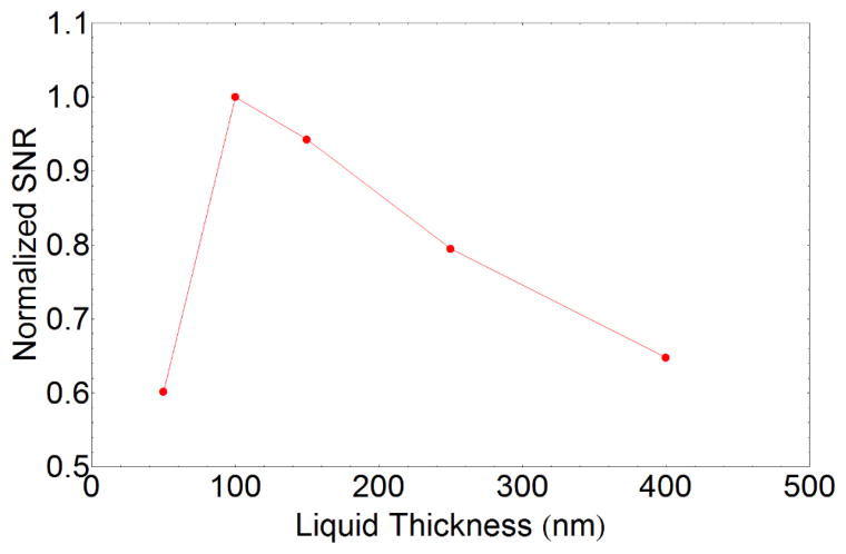
Next, we consider the constraints that must be satisfied to enable quantitative, high-resolution EELS to be performed. First we focus on the design criteria for obtaining EELS of the liquid (rather than a solid particle in the liquid). At liquid layer thicknesses, t, much less than the inelastic scattering length, λ, the liquid EELS signal will be small compared to that from the membranes, while at large thicknesses (t/λ > 3) plural scattering obscures both the valence and core-loss regions. A good EELS signal can be therefore be obtained if, while minimizing multiple scattering, each electron experiences an average of one inelastic scattering event, i.e., t/λ should be ≈ 1. To make a more detailed estimate of the optimal liquid thickness we calculate the expected SNR of the O K core-loss edge using simulated EEL spectra assuming the atomic density of oxygen for water. The SNR is determined by calculating the expected O K signal over a 30 eV window using hydrogenic cross sections while the noise is calculated from the square root of the intensity under the same window, including the background contribution. The background intensity is given by the sum of the energy losses due to the Si L edge at 99 eV, the N K edge at 402 eV and the combined multiple scattering from core loss and plasmon losses. To approximate the background intensity including multiple scattering, the core-loss spectrum from the SiNx membrane is simulated and convoluted with a simulated low-loss spectrum. The low-loss spectrum is simulated as a series of Gaussian plasmon peaks where the total plasmon intensity is determined by Poisson statistics for a given t/λ. The value of t/λ used is the total value for the membranes and liquid, again calculated using the Iakoubovskii approximation.(Iakoubovskii, et al., 2008) All of the calculations are performed using programs created by Egerton;(Egerton, 2011) the core-loss edges are approximated by using the Sigmal3 and Sigmak3 hydrogenic cross section programs and the low-loss is simulated by the SpecGen program. Similar calculations for different types of samples have been performed previously (Egerton, 2011; Menon & Krivanek, 2002) to estimate detection limits in EELS and analyze the relationship between SNR and thickness. The simulations indicate an optimal O K SNR for a liquid thickness of ≈ 100 nm which corresponds to a total t/λ value of 0.9 (figure 1). For low-loss EELS where energy-loss features from the liquid and the membrane will overlap, the membrane thickness should be minimized as far as possible within the constraints imposed by the need to prevent mechanical deformation or fracture and the limits of the fabrication approach. Previously, core-loss EELS from liquids has been performed in thicker liquid cells, but the quality of the spectra was limited by the low SNR. Holtz, et al. were able to detect only a small O K peak for the thinnest liquid layer (t/λ ≈ 3), but were able to obtain useful information from the low-loss signal for even thicker liquid layers (Holtz, et al., 2013). Jungjohann, et al., reported O K EELS data from ≈ 200 nm of water showing transient near-edge structure that was interpreted as being caused by radiolysis (Jungjohann, et al., 2012). Both of these reports are consistent with the analysis of simulated spectra in this study.
Figure 1.
Estimated SNR normalized to the maximum value for the O K edge as a function of liquid thickness for a cell with two 50 nm SiN membranes. Optimal liquid thickness for studying the O K edge of liquids is ≈ 100 nm.
To estimate the capabilities of this liquid cell for core-loss spectroscopy of a nanoparticle in liquid, we calculated the expected SNR for Fe2O3 for a cell with a 250 nm thick liquid layer and estimate that a 2 nm thick nanoparticle should produce a detectable signal for 1 nA of beam current, a 5 s dwell time and a 20 eV window over the Fe L2,3 edge.
The liquid layer thickness can be adjusted during the fabrication over a wide range, depending on whether spectroscopic information is needed from the liquid itself, or from nanoparticles in solution; thinner liquid layers being preferred for EELS analysis of nanoparticles and thicker layers for EELS of the liquid. Reducing the liquid-layer thickness below a certain value, however, will not be worthwhile if the membrane thickness cannot be reduced because the scattering from the membrane will determine the SNR for small liquid layer thicknesses.
For EELS analysis of the low-loss region for liquids where features from the membrane and the liquid will overlap it will be advantageous for low-loss scattering from the liquid to dominate, requiring that the liquid t/λ be greater than that of the membrane, making the assumption that λ is determined primarily by the low-loss intensity. For 50 nm SiNx membranes and water, the liquid layer thickness should be at least 130 nm. Low-loss intensity from the membrane can be removed from a spectrum of the liquid by deconvolving a membrane-only reference spectrum (Egerton, et al., 2008; Wang, et al., 2009a), though there will always be some loss in SNR.
Ultimately, the precise values of the desired liquid thickness will depend on the liquid or nanoparticles being studied and the experiment to be conducted. Using calculations of SNR for the O K edge from water gives an optimal liquid thickness of ≈ 100 nm and based on considerations for low-loss spectroscopy the liquid thickness should be at least 130 nm. A good target liquid thickness for EELS is then in the range of 100 nm to 200 nm. In this thickness range the Fe L signal should be detectable for hematite nanoparticles ≈ 2 nm in thickness.
There is a limit to how small a membrane thickness can be used. Clearly the cell must be robust against catastrophic failure. SiN membranes have high strength and exhibit a high level of fracture toughness (Liddle, et al., 1994) and are therefore a suitable choice. As noted above, it is also necessary to maintain a thin, uniform liquid layer. In typical cell designs, the membranes are unsupported across the viewing area (supported only at the edges of the window in the Si wafer) and are subject to pressure-driven bulging. The relationship between membrane deflection and pressure, for a square membrane, is given by (Liddle, et al., 1994; Maier-Schneider, et al., 1995):
| (1) |
where σ0 is the initial stress in the membrane, E the Young’s modulus, ν the Poisson’s ratio, t the thickness, a the half-width of the membrane, and δ the deflection (note that for a given value of a, the deflection is approximately a factor of 2 larger for a long rectangular membrane). Equation 1 is only valid for the situation when the thickness t is much smaller than the half-width, a; for smaller widths, finite-element analysis (FEA) is necessary. The options for controlling the deflection are limited: the size of membrane, a, can be reduced, or the initial stress increased.
Reducing the width of the membrane below approximately 20 μm is impractical for fabrication reasons (typical wafer thickness variations cause membrane widths to vary by as much as a factor of two at these sizes), while the initial stress cannot be increased above 1 GPa without compromising the strength of the membrane (Liddle, et al., 1994). Even for a long rectangular SiN membrane of width 20 μm, thickness 50 nm, and initial stress of 0.3 GPa, the center deflection for each membrane will be approximately 140 nm under 1 atmosphere, translating to an undesirable liquid layer thickness variation of more than 200 % for an initial cavity thickness of 100 nm.
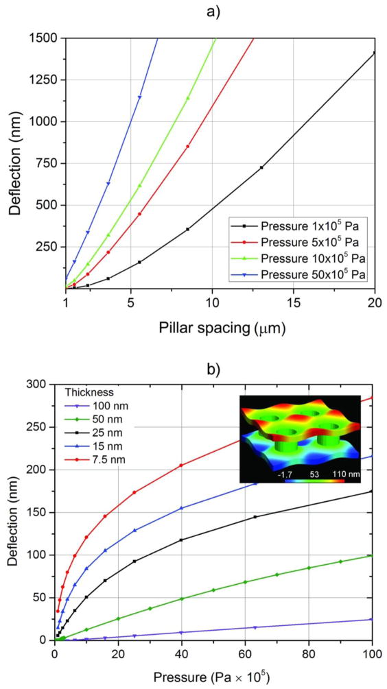
Instead of reducing the total membrane width to the level of a few micrometers, a more suitable alternative to achieve the desired small membrane deflections is to introduce regular support structures to periodically connect the upper and lower membranes, equivalent to reducing the width, a, in equation 1, while permitting the total membrane width and viewing area to remain large (hundreds of micrometers). Two groups (Grogan & Bau, 2010; Mele, et al., 2010) have pursued wafer bonding techniques for sealing two-piece cells with supports, but uniform contact and bonding, membrane bowing and stress-induced membrane rupture remain problematic. The most promising method to control membrane deflection under pressure, both in terms of performance and ease of fabrication, is the use of a monolithic cell (Mele, et al., 2010). FEA calculations for a pillar-supported, monolithic cell show that membrane deflections can be reduced to acceptable levels (≲ 20 nm for ≈ 105 Pa (1 atm) pressure) once the pillar-to-pillar separation is reduced below 2 μm to 3 μm (figure 2). This decouples the size of the viewing area from membrane deflection and enables precise control over the liquid layer thickness.
Figure 2.
a) Membrane deflection as a function of pillar spacing for different pressures. b) Membrane deflection as a function of pressure for membranes of different thicknesses and a constant pillar edge-to-edge spacing of 1 μm. In all cases the initial membrane stress is 180 MPa. The inset shows a finite element simulation of the deflections of a structure with a membrane thickness of 50 nm and a support pillar pitch and edge-to-edge spacing of 2 μm and 1 μm respectively. The vertical displacements in the image are exaggerated by 5 × for clarity.
Materials and Methods
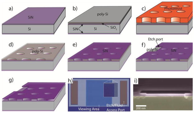
The cell is fabricated by first depositing a layer of SiN, followed by a layer of silicon oxide and a layer of polysilicon. Holes are then etched through the poly-Si/SiO2 bilayer to the underlying SiN before the second SiN membrane layer is deposited (Figure 3a). Two etch ports are opened in the upper layer of SiN on either side of the viewing area, and out of the electron beam path. A hot KOH etch is then used to leach out the poly-Si/SiO2 bilayer, leaving a cavity with a precisely controlled height. Because SiN etches very slowly as compared to Si in KOH (3.3 nm/h versus 2.2 μm/min), lateral etches over hundreds of micrometers are possible in a relatively short time (≈ 2 hours), without compromising the SiN membranes, enabling the creation of cells with large viewing areas. The etch ports also serve as in/outlets for a microfluidic system.
Figure 3.
Fabrication of the liquid cell. a) LPCVD SiN is deposited on both sides of a Si wafer. b) Deposition of sacrificial bilayer of poly-Si/SiO2. The poly-Si etches laterally rapidly in KOH, leaving the thin SiO2 layer to be etched vertically. The SiO2 layer acts as a protective layer should metal patterns be used on the lower SiN layer. c) Bilayer patterning via photolithography and reactive ion etching. d) Photoresist removal. e) Second LPCVD SiN deposition. f) Etch ports formed in upper SiN layer by photolithography and reactive ion etch. g) Removal of sacrificial layer by KOH etch. h) Optical micrograph of completed device (overall width = 2 mm). Inset shows higher magnification view of pillar-supported membrane. Pillar spacing is 1 μm edge-to-edge. i) Scanning electron microscope image of cross-section of cavity between two pillars.
The small spacing between the membrane supports not only helps to keep deflections at the few-nanometer level (< 10 nm) when the cell is in operation, it also serves to prevent capillary forces from collapsing and sticking together the membranes when the cell is dried after etching, or when fluid is introduced during sample loading. The Young-Laplace pressure for a cylindrical meniscus of radius r and surface energy γ is γ/r. For water (γ = 0.073 J/m2 at 20 °C) the pressure difference across the meniscus in a 100 nm tall cavity is approximately 1.5 × 10⁶ Pa (15 atm). Using Equation (1) and ignoring corrections for large deflections, this constrains the maximum distance between supports to be less than 3 μm for 100 nm thick membranes. An attractive feature of such a cell is its ability to support very high pressures – up to 5 × 10⁶ Pa (≈ 50 atm) before there is any danger of the membrane breaking. This may permit the observation of catalytic processes that occur at high pressure. Once completed, the cells can be loaded via a pulled-glass micropipette and filled by capillary action through the etch ports. The cells may then be sealed with UV-curing resin, or, if fluid flow is desired, with a microfluidic system.
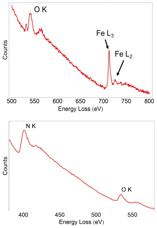
In order to demonstrate the capabilities of the cell, we have performed high-resolution imaging in both TEM and STEM modes using suspensions of Ag nanoparticles in water/isopropanol mixtures, and collected images and EELS data from Fe2O3 nanorods in water/ethanol. The data were collected at 300 keV using both an ETEM equipped with an aberration corrector for the image-forming lens and a non-corrected TEM, both with imaging filters, and with the liquid cell in static (no-flow) mode. The HRTEM images were collected with a parallel beam (convergence semi-angle α = 0 mrad) on the aberration-corrected ETEM. The HR-STEM images were collected using an annular dark-field detector with collection semi-angles between 30 mrad and 75 mrad, and a condenser aperture-spot size combination capable of a nominal resolution of 0.136 nm. EELS data in STEM mode (shown in figure 7a) were collected with a collection semi-angle β = 21 mrad and convergence semi-angle α = 10 mrad. Additional EELS data were also acquired in TEM mode with α = 2.6 mrad and β = 9.6 mrad (shown in figure 7b). EELS data acquired under these conditions were also used to calculate the hematite nanorod oxidation state.
Figure 7.
a) Core-loss EELS spectrum of an iron oxide nanoparticle in liquid. The ratio between the L2 and L3 peaks enables the identification of the iron oxidation state as Fe3+. b) Core-loss EELS spectrum from the liquid showing an N peak from the SiN membrane and an O peak generated primarily by the liquid.
Results and Discussion
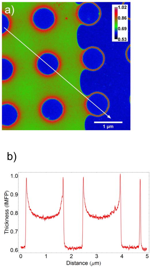
Figure 4a is a thickness map of a liquid-filled cell near a boundary with a vapor-containing region and a line profile of the map is shown in figure 4b. The regular array of support pillars is seen and the liquid region is on the left-hand side of the image. The thickness profile indicates that the membranes are actually bowed inward, rather than outward, due to the capillary force of the liquid. The t/λ value in the liquid region decreases from ≈ 0.9 near the pillar to ≈ 0.8 between the pillars. Using a known value of the liquid thickness near the pillar and accounting for the 100 nm of SiN in the beam path indicates a λ value of ≈ 330 nm for the liquid mixture of water and ethanol. This value is significantly larger than values calculated for liquid water using various approximations derived from measurements on solids and we note that the experimentally measured value from Klein et al. (also for 300 kV) for liquid water is ≈ 400 nm (Klein, et al., 2011b). Using this λ value we can deduce a variation in the liquid layer thickness from 90 nm to 66 nm going from the pillar edge to between the pillars. No significant variation in these values was measurable across the entire cell viewing area.
Figure 4.
a) Energy-filtered TEM t/λ map of a cell partially-filled with a water/isopropanol mixture showing the liquid meniscus. The calibration bar is in units of t/λ. b) Thickness profile taken along the line in a) (IMFP: Inelastic mean free path). The maximum reduction in liquid layer thickness caused by capillary forces in the liquid-filled region is approximately 25 nm. The deflection in the vapor-filled region at 105 Pa (≈ 1 atm) is negligible.
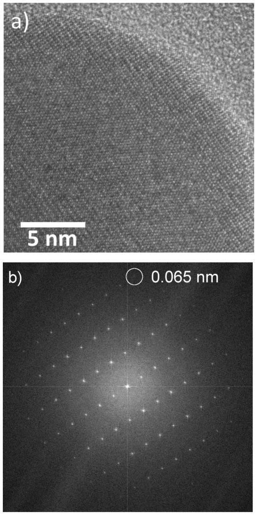
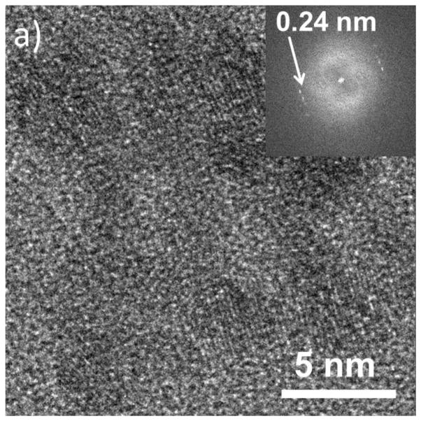
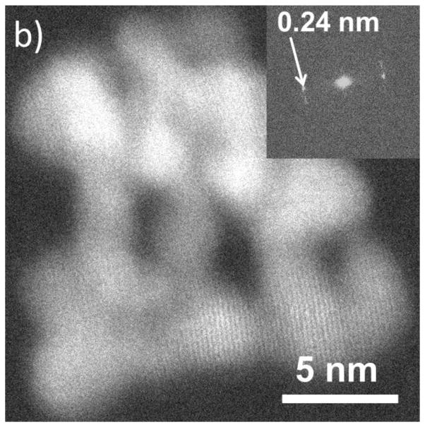
Figure shows the HRTEM image and corresponding fast Fourier transform (FFT) demonstrating lattice fringes out to 0.065 nm of a ≈ 40 nm diameter Fe2O3 nanorod. The image was acquired with a total SiN thickness of 100 nm, and a liquid-layer thickness of ≈ 80 nm (≈ 40 nm over the nanorod) in the beam path. 10 frames were aligned and summed for the image to improve the SNR giving a total acquisition time of 2.5 s. The membrane and liquid contribute a background and noise, but do not prevent high-resolution imaging. We note that the observation of a peak in the FFT corresponding to 0.065 nm does not indicate a resolution of 0.065 nm, but does demonstrate good stability of the system (O’Keefe, et al., 2008; O’Keefe, et al., 2010). Typically, for thick liquid cells, the best resolution in TEM mode is achieved for particles on the lower membrane, while the opposite is true for STEM (Klein, et al., 2011a). This “top-bottom” effect has been previously demonstrated for imaging of metal particles on polystyrene spheres (Reimer, 1997). For a particle on the bottom membrane, beam broadening in the upper membrane and liquid degrades the STEM resolution; in TEM mode, the image of a particle on the upper membrane is degraded by broadening as the electrons pass through the liquid and lower membrane. STEM images using an annular dark-field (ADF) detector offer better signal-to-noise than TEM images for thick samples and have therefore been preferred previously for imaging in thick liquid layers. In order to explore the range of applicability of the top-bottom criterion we have performed lattice imaging in both STEM and TEM modes at various locations across the cell membrane area and we find that lattice resolution is attainable on the same object in both TEM and STEM, repeatedly and reproducibly. Figure shows an example of a cluster of Ag nanoparticles exhibiting 0.24 nm lattice fringes ((111) planes of Ag) in both TEM and STEM images. This demonstrates that the “top-bottom” effect is negligible for an appropriately designed cell.
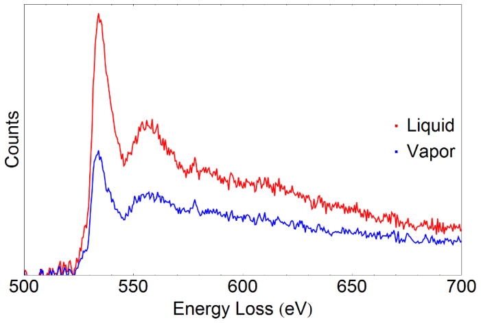
Both core-loss and low-loss EELS on particles in liquid and liquids alone are possible with the cell. Figure a shows EELS data obtained from a ≈ 40 nm diameter Fe2O3 nanorod in water/isopropanol acquired with a total exposure time of 20 s. Near-edge fine structure is observable in both the O K edge at 532 eV and the Fe L2,3 edge at 708 eV despite the background from the liquid and membranes. Quantification of the Fe oxidation state is possible by measurement of the Fe L white-line ratio. The method of white-line quantification described by Cavé et al. (Cavé, et al., 2006) was applied to a spectrum from a hematite nanorod obtained with a 0.1 eV/channel dispersion; after background subtraction and Richardson-Lucy deconvolution (Egerton, et al., 2008) with the low-loss spectrum, a double arctan function was used to subtract the continuum contribution under the white lines and the integrated intensity for the L2 and L3 peaks was obtained with 2 eV windows. The calculated L3:L2 ratio is 5.67 ± 0.1 (uncertainty is given as ± one standard deviation), in very good agreement with the value for Fe2O3 of 5.64 ± 0.1 reported by Cavé et al. (Cavé, et al., 2006) The uncertainty estimates are determined by assuming the uncertainty in the intensity values for each peak is given by the square root of the intensity (Poisson statistics). The uncertainty reported by Cavé et al. was the standard deviation from multiple measurements on a hematite standard. Noise contributed from the increased background intensity will increase the quantification uncertainty relative to measurements in high-vacuum conditions. However, this confirms that quantitative analysis of the near-edge structure from particles within a liquid cell is possible. Figure b shows core-loss EELS data from a liquid mixture of water and ethanol. In the core-loss spectrum the N K edge from the membrane is visible as well as a small O K edge primarily from the liquid. The membrane also contributes to the O K edge, but detailed comparison between spectra from empty cells (membranes only) and from cells filled with the ethanol-water mixture indicates the O K intensity increases by more than a factor of 2 when the cell is filled with liquid. Figure 8 shows two spectra from a cell filled with a water/ethanol mixture, one from a liquid-containing region and one from a nearby vapor-filled region; after deconvolution with the low-loss spectrum and normalization of the intensities, it is possible to determine the O K contribution from the liquid itself. The thin vapor layer in parts of the cell contributes a negligible O signal so the O signal from the vapor region is from O in the membranes.
Figure 8.
O K edge EELS data from a liquid-containing region and a vapor-containing region of the same liquid cell after deconvolution and intensity normalization. Some of the O K signal (the vapor spectrum) comes from the SiNx membranes.
It is worthwhile to note that vapor formation during imaging can create small regions of vapor under the beam and this process can ultimately limit the time available for data acquisition from a sample in liquid. Although this was occasionally observed during imaging with this cell, the data shown here were not acquired from regions where bubble formation occurred.
Conclusions
In conclusion, we have designed and fabricated a monolithic liquid cell for in situ imaging and spectroscopy in thin liquid layers in the TEM. We have demonstrated 0.24 nm resolution in the same region of liquid in both STEM and TEM modes repeatedly and reproducibly, and the ability to perform quantitative core-loss EELS. The ability to maintain a thin liquid layer is the key enabler for this accomplishment. Additional benefits of this new design are the fact that the TEM viewing area and liquid thickness are independently adjustable, and the ability of the cell to withstand pressure differentials well in excess of one atmosphere.
Figure 5.
a) HRTEM image of an Fe2O3 nanorod. b) Fourier transform of the image in a) demonstrating the presence of lattice fringes out to a spacing of 0.065 nm.
Figure 6.
a) HRTEM image of an Ag nanoparticle cluster in liquid. b) HRSTEM images of the same cluster imaged in a). Both images show lattice-fringe resolution of 0.24 nm. The insets are the Fast Fourier Transforms of the images demonstrating the resolution.
Acknowledgments
Dr. Mihaela Tanase acknowledges support under the National Institute for Standards and Technology American Recovery and Reinvestment Act Measurement Science and Engineering Fellowship Program Award 70NANB10H026 through the University of Maryland.
ABBREVIATIONS
- TEM
transmission electron microscopy
- HRTEM
high resolution transmission electron microscopy
- EELS
electron energy loss spectroscopy
- SNR
signal-to-noise ratio
References
- Abrams IM, McBain JW. A Closed Cell for Electron Microscopy. Journal of Applied Physics. 1944;15(8):607–609. doi: 10.1126/science.100.2595.273. [DOI] [PubMed] [Google Scholar]
- Baker RTK, Harris PS. Controlled atmosphere electron microscopy. Journal of Physics E: Scientific Instruments. 1972;5(8):793. [Google Scholar]
- Bartholomew CH, Farrauto RJ. Fundamentals of Industrial Catalytic Processes. Wiley; 2011. [Google Scholar]
- Bell AT. The Impact of Nanoscience on Heterogeneous Catalysis. Science. 2003;299(5613):1688–1691. doi: 10.1126/science.1083671. [DOI] [PubMed] [Google Scholar]
- Burge RE, Misell DL. Electron Energy Loss Spectra for Evaporated Carbon Films. Philosophical Magazine. 1968;18(152):251–259. [Google Scholar]
- Cavé L, Al T, Loomer D, Cogswell S, Weaver L. A STEM/EELS method for mapping iron valence ratios in oxide minerals. Micron. 2006;37(4):301–309. doi: 10.1016/j.micron.2005.10.006. [DOI] [PubMed] [Google Scholar]
- Chen Q, Smith JM, Park J, Kim K, Ho D, Rasool HI, Zettl A, Alivisatos AP. 3D Motion of DNA-Au Nanoconjugates in Graphene Liquid Cell Electron Microscopy. Nano Letters. 2013;13(9):4556–4561. doi: 10.1021/nl402694n. [DOI] [PubMed] [Google Scholar]
- Cosslett VE. Energy loss and chromatic aberration in electron microscopy. Zeitschrift fur Angewandte Physik. 1969;27:138–141. [Google Scholar]
- Creemer JF, Helveg S, Hoveling GH, Ullmann S, Molenbroek AM, Sarro PM, Zandbergen HW. Atomic-scale electron microscopy at ambient pressure. Ultramicroscopy. 2008;108(9):993–998. doi: 10.1016/j.ultramic.2008.04.014. [DOI] [PubMed] [Google Scholar]
- de Jonge N, Peckys DB, Kremers GJ, Piston DW. Electron microscopy of whole cells in liquid with nanometer resolution. Proceedings of the National Academy of Sciences. 2009 doi: 10.1073/pnas.0809567106. [DOI] [PMC free article] [PubMed] [Google Scholar]
- de Jonge N, Poirier-Demers N, Demers H, Peckys DB, Drouin D. Nanometer-resolution electron microscopy through micrometers-thick water layers. Ultramicroscopy. 2010;110(9):1114–1119. doi: 10.1016/j.ultramic.2010.04.001. [DOI] [PMC free article] [PubMed] [Google Scholar]
- de Jonge N, Ross FM. Electron microscopy of specimens in liquid. Nat Nano. 2011;6(11):695–704. doi: 10.1038/nnano.2011.161. [DOI] [PubMed] [Google Scholar]
- Dukes MJ, Jacobs BW, Morgan DG, Hegde H, Kelly DF. Visualizing nanoparticle mobility in liquid at atomic resolution. Chemical Communications. 2013;49(29):3007–3009. doi: 10.1039/c3cc41136b. [DOI] [PubMed] [Google Scholar]
- Egerton RF. Electron energy-loss spectroscopy in the electron microscope. Berlin; New York: Springer; 2011. [Google Scholar]
- Egerton RF, Wang F, Malac M, Moreno MS, Hofer F. Fourier-ratio deconvolution and its Bayesian equivalent. Micron. 2008;39(6):642–647. doi: 10.1016/j.micron.2007.10.004. [DOI] [PubMed] [Google Scholar]
- Frances MR. Controlling nanowire structures through real time growth studies. Reports on Progress in Physics. 2010;73(11):114501. [Google Scholar]
- Gai P. Developments in in situ Environmental Cell High-Resolution Electron Microscopy and Applications to Catalysis. Topics in Catalysis. 2002;21(4):161–173. [Google Scholar]
- Grogan JM, Bau HH. The Nanoaquarium: A Platform for In Situ Transmission Electron Microscopy in Liquid Media. Microelectromechanical Systems, Journal of. 2010;19(4):885–894. [Google Scholar]
- Holtz ME, Yu Y, Gao J, Abruña HD, Muller DA. In Situ Electron Energy-Loss Spectroscopy in Liquids. Microscopy and Microanalysis. 2013;19(04):1027–1035. doi: 10.1017/S1431927613001505. [DOI] [PubMed] [Google Scholar]
- Iakoubovskii K, Mitsuishi K, Nakayama Y, Furuya K. Thickness measurements with electron energy loss spectroscopy. Microscopy Research and Technique. 2008;71(8):626–631. doi: 10.1002/jemt.20597. [DOI] [PubMed] [Google Scholar]
- Jeangros Q, Faes A, Wagner JB, Hansen TW, Aschauer U, Van herle J, Hessler-Wyser A, Dunin-Borkowski RE. In situ redox cycle of a nickel–YSZ fuel cell anode in an environmental transmission electron microscope. Acta Materialia. 2010;58(14):4578–4589. [Google Scholar]
- Jungjohann KL, Evans JE, Aguiar JA, Arslan I, Browning ND. Atomic-Scale Imaging and Spectroscopy for In Situ Liquid Scanning Transmission Electron Microscopy. Microscopy and Microanalysis. 2012;18(03):621–627. doi: 10.1017/S1431927612000104. [DOI] [PubMed] [Google Scholar]
- Klein K, Anderson I, De Jonge N. Transmission electron microscopy with a liquid flow cell. Journal of microscopy. 2011a;242(2):117–123. doi: 10.1111/j.1365-2818.2010.03484.x. [DOI] [PubMed] [Google Scholar]
- Klein K, de Jonge N, Anderson I. Energy-Loss Characteristics for EFTEM Imaging with a Liquid Flow Cell. Microscopy and Microanalysis. 2011b;17(Supplement S2):780–781. [Google Scholar]
- Liao HG, Zherebetskyy D, Xin H, Czarnik C, Ercius P, Elmlund H, Pan M, Wang LW, Zheng H. Facet development during platinum nanocube growth. Science. 2014;345(6199):916–919. doi: 10.1126/science.1253149. [DOI] [PubMed] [Google Scholar]
- Liddle JA, Huggins HA, Mulgrew P, Harriott LR, Wade HH, Bolan K. Fracture Strength of Thin Ceramic Membranes. MRS Online Proceedings Library. 1994;338 null-null. [Google Scholar]
- Liu KL, Wu CC, Huang YJ, Peng HL, Chang HY, Chang P, Hsu L, Yew TR. Novel microchip for in situ TEM imaging of living organisms and bio-reactions in aqueous conditions. Lab on a Chip. 2008;8(11):1915–1921. doi: 10.1039/b804986f. [DOI] [PubMed] [Google Scholar]
- Maier-Schneider D, Maibach J, Obermeier E. A new analytical solution for the load-deflection of square membranes. Microelectromechanical Systems, Journal of. 1995;4(4):238–241. [Google Scholar]
- Marton L. La microscopie electronique des objets biologiques. Bull de L’Acad Royale de Belgique. 1935;21:553–560. [Google Scholar]
- Mele L, Santagata F, Pandraud G, Morana B, Tichelaar FD, Creemer JF, Sarro PM. Wafer-level assembly and sealing of a MEMS nanoreactor for in situ microscopy. Journal of Micromechanics and Microengineering. 2010;20(8):085040. [Google Scholar]
- Menon NK, Krivanek OL. Synthesis of Electron Energy Loss Spectra for the Quantification of Detection Limits. Microscopy and Microanalysis. 2002;8(03):203–215. doi: 10.1017/s1431927602020111. [DOI] [PubMed] [Google Scholar]
- O’Keefe M, Allard L, Blom D. Young’s Fringes Are Not Evidence of HRTEM Resolution. Microscopy and Microanalysis. 2008;14(Supplement S2):834–835. [Google Scholar]
- O’Keefe M, Allard L, Blom D. Defining HRTEM Resolution: Image Resolutions and Microscope Limits. Microscopy and Microanalysis. 2010;16(Supplement S2):766–767. [Google Scholar]
- Radisic A, Ross FM, Searson PC. In Situ Study of the Growth Kinetics of Individual Island Electrodeposition of Copper. The Journal of Physical Chemistry B. 2006a;110(15):7862–7868. doi: 10.1021/jp057549a. [DOI] [PubMed] [Google Scholar]
- Radisic A, Vereecken PM, Hannon JB, Searson PC, Ross FM. Quantifying Electrochemical Nucleation and Growth of Nanoscale Clusters Using Real-Time Kinetic Data. Nano Letters. 2006b;6(2):238–242. doi: 10.1021/nl052175i. [DOI] [PubMed] [Google Scholar]
- Ramachandra R, Demers H, de Jonge N. The influence of the sample thickness on the lateral and axial resolution of aberration-corrected scanning transmission electron microscopy. Microscopy and microanalysis. 2013;19(1):93–101. doi: 10.1017/S143192761201392X. [DOI] [PubMed] [Google Scholar]
- Reimer L. Transmission Electron Microscopy: Physics of Image Formation and Microanalysis. New York: Springer-Verlag; 1997. [Google Scholar]
- Sharma R. Design and Applications of Environmental Cell Transmission Electron Microscope for In Situ Observations of Gas–Solid Reactions. Microscopy and Microanalysis. 2001;7(06):494–506. doi: 10.1017.S1431927601010480. [DOI] [PubMed] [Google Scholar]
- Sharma R, Crozier† PA, Kang ZC, Eyring L. Observation of dynamic nanostructural and nanochemical changes in ceria-based catalysts during in-situ reduction. Philosophical Magazine. 2004;84(25–26):2731–2747. [Google Scholar]
- Sharma R, Rez P, Brown M, Du G, Treacy MMJ. Dynamic observations of the effect of pressure and temperature conditions on the selective synthesis of carbon nanotubes. Nanotechnology. 2007;18(12):125602. [Google Scholar]
- Swift JA, Brown AC. An environmental cell for the examination of wet biological specimens at atmospheric pressure by transmission scanning electron microscopy. Journal of Physics E: Scientific Instruments. 1970;3(11):924. doi: 10.1088/0022-3735/3/11/426. [DOI] [PubMed] [Google Scholar]
- Vendelbo SB, Elkjær CF, Falsig H, Puspitasari I, Dona P, Mele L, Morana B, Nelissen BJ, van Rijn R, Creemer JF, Kooyman PJ, Helveg S. Visualization of oscillatory behaviour of Pt nanoparticles catalysing CO oxidation. Nat Mater. 2014 doi: 10.1038/nmat4033. advance online publication. [DOI] [PubMed] [Google Scholar]
- Wang C, Qiao Q, Shokuhfar T, Klie RF. High-Resolution Electron Microscopy and Spectroscopy of Ferritin in Biocompatible Graphene Liquid Cells and Graphene Sandwiches. Advanced Materials. 2014;26(21):3410–3414. doi: 10.1002/adma.201306069. [DOI] [PubMed] [Google Scholar]
- Wang F, Egerton R, Malac M. Fourier-ratio deconvolution techniques for electron energy-loss spectroscopy (EELS) Ultramicroscopy. 2009a;109(10):1245–1249. doi: 10.1016/j.ultramic.2009.05.011. [DOI] [PubMed] [Google Scholar]
- Wang R, Crozier PA, Sharma R. Structural Transformation in Ceria Nanoparticles during Redox Processes. The Journal of Physical Chemistry C. 2009b;113(14):5700–5704. [Google Scholar]
- Welch DA, Faller R, Evans JE, Browning ND. Simulating realistic imaging conditions for in situ liquid microscopy. Ultramicroscopy. 2013;135(0):36–42. doi: 10.1016/j.ultramic.2013.05.010. [DOI] [PMC free article] [PubMed] [Google Scholar]
- Williamson MJ, Tromp RM, Vereecken PM, Hull R, Ross FM. Dynamic microscopy of nanoscale cluster growth at the solid-liquid interface. Nat Mater. 2003;2(8):532–536. doi: 10.1038/nmat944. [DOI] [PubMed] [Google Scholar]
- Yuk JM, Park J, Ercius P, Kim K, Hellebusch DJ, Crommie MF, Lee JY, Zettl A, Alivisatos AP. High-Resolution EM of Colloidal Nanocrystal Growth Using Graphene Liquid Cells. Science. 2012;336(6077):61–64. doi: 10.1126/science.1217654. [DOI] [PubMed] [Google Scholar]
- Zheng H, Smith RK, Jun Y-w, Kisielowski C, Dahmen U, Alivisatos AP. Observation of Single Colloidal Platinum Nanocrystal Growth Trajectories. Science. 2009;324(5932):1309–1312. doi: 10.1126/science.1172104. [DOI] [PubMed] [Google Scholar]


