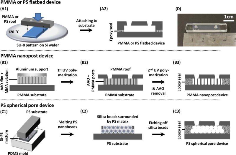
Figure 1.

Schematics showing the fabrication processes of (A) PMMA and PS flatbed devices, (B) PMMA nanopost devices, and (C) PS spherical pore devices. (A1) A microchannel was formed on the substrate by manual embossing. (A2) The open channel was attached to a second flat sheet of the same material by epoxy glue, creating a flatbed microchannel. (B1) An array of PMMA nanoposts was fabricated through polymerizing MMA in an AAO template. (B2) The aluminum support was chemically removed and the newly opened top was attached to a PMMA roof by MMA and UV-polymerization. (B3) The PMMA nanopost device was created after chemically removing the AAO and sealing the sides. (C1) A binary suspension of silica and PS was deposited onto a PDMS mold. The PS beads were melted and glued to a PS substrate. (C2) The PDMS mold was detached and silica beads were etched away. (C3) A PS roof was attached to the PS porous structure and the sides were sealed, creating a PS spherical pore device. (D) Photograph of a typical microfluidic device containing nanopost arrays and inlet/outlet ports. Devices with spherical pores have a similar appearance.
