Abstract
One-dimensional heterogeneous nanostructures in the form of ZnO-coated TiO2 nanotubes (ZnO/TiO2 NTs) were fabricated by atomic layer deposition of an ultrathin ZnO coating on electrochemical anodization-formed TiO2 nanotubes (NTs) with the thickness of ZnO coating being precisely controlled at atomic scale, and the photoelectrochemical activity of the fabricated ZnO/TiO2 NTs and the influence of ZnO coating and its thickness were studied. The structures of TiO2 NTs and ZnO coatings were characterized by X-ray diffraction, Raman backscattering spectroscopy, and transmission electron microscopy. The photoelectrochemical activity was studied through the measurements of electrochemical impendence, flat-band potential, and transient photocurrent density. The TiO2 NTs exhibit anatase structure, and the ZnO coatings are structured with hexagonal wurtzite. The photoelectrochemical activity of the ZnO/TiO2 NTs is strongly dependent on the thickness of ZnO coating. ZnO/TiO2 NTs with a thinner rather than a thicker ZnO coating exhibit better photoelectrochemical activity with reduced charge transfer resistance, increased negative flat-band potentials, and enhanced photocurrent densities. Under visible illumination, an increase of about 60 % in the photoelectrochemical activity is obtained for ZnO/TiO2 NTs with an about 2-nm-thick ZnO coating.
Keywords: Photoelectrochemical activity, Heterogeneous nanostructure, TiO2, ZnO, ZnO-coated TiO2 nanotube
Background
Titania (TiO2) and zinc oxide (ZnO) have recently attracted much attention because of their excellent optical, photoelectronic, and photoelectrochemical properties and consequently their potential applications in wide fields including photocatalytic reactions and photovoltaic processes [1–5]. Both metal oxides also have advantages of low cost, physical and chemical stability, nontoxicity, and ease of availability. In addition, TiO2 and ZnO have similar band-gap energies (~3.22 eV for TiO2 and ~3.37 eV for ZnO) and are compatible to each other to compose heterogeneous materials. A variety of heterostructured materials composed of TiO2 and ZnO (TiO2-ZnO) have been reported. Heterogeneous TiO2-ZnO materials exhibit improved individual and combined properties which are very distinct from those of the single constituting materials TiO2 and ZnO and are promising for applications such as photocatalytic reactions and photovoltaic processes. Dye-sensitized solar cells using ZnO-coated nanocrystalline TiO2 films as electrodes, for example, have shown enhanced conversion efficiencies [6]. In particular for heterostructured TiO2-ZnO, nanoscaled TiO2 and ZnO are superior to bulk and film materials in their large surface-to-volume ratio for a large interface between TiO2 and ZnO. Therefore, nanosized heterostructures constructed of nanoscaled TiO2 and ZnO show better photoelectronic, photochemical, and photoelectrochemical properties. When used as a photocatalyst or a photoelectrode, for example, heterogeneous ZnO-TiO2 nanostructures can provide improved performance due to the combination of the high activity of TiO2 with the high electron mobility of ZnO. Furthermore, the alignment of the staggered band gaps of TiO2 and ZnO is favorable for the separation of electrons and holes and consequently the suppression of electron-hole recombination [7, 8]. The staggered band alignment also results in an extension for spectral range of photoresponse, which allows an efficient use of light with a wide spectral band [9, 10]. Therefore, better electrochemical and photoelectrochemical properties and hence enhanced photocatalytic activities and increased photovoltaic efficiencies can be expected for the heterogeneous ZnO-TiO2 nanostructures because of their improved charge conductivity, enhanced charged carrier separation, and extended photoresponse range [11, 12]. Of the diverse ZnO-TiO2 nanoheterostructures, one-dimensional (1D) nanogeometry has received particular attention in the photocatalytic and photovoltaic applications due to its superior charge transport ability and short recombination pathway, which significantly suppresses the recombination of photogenerated electrons and holes [13–16]. The ultraviolet (UV) photoconductivity and photosensitivity of TiO2-coated ZnO nanorods have been reported to be largely enhanced [17]. Using ZnO-sheathed TiO2 as photoanodes, dye-sensitized solar cells have shown enhanced performance [18]. ZnO-coated TiO2 nanotube (ZnO/TiO2 NT) is one of the most studied 1D heterogeneous ZnO-TiO2 nanostructures [16, 19–21]. However, the optimized photocatalytic activity and photovoltaic efficiency of heterogeneous TiO2-ZnO materials including 1D heterogeneous ZnO-TiO2 nanostructures are strongly dependent on the morphology and geometry.
In comparison to bare TiO2 NTs, TiO2 NTs covered by a thin ZnO coating usually present improved electrochemical and photoelectrochemical properties and are expected to have high quantum efficiencies for photocatalytic reactions and photovoltaic processes [16, 19–21]. As a nanoscaled heterostructure, it has been proved that the properties of ZnO/TiO2 NTs are strongly dependent on the geometry and morphology of the heterogeneous nanostructure, the crystal structure of TiO2 and ZnO, and the interfacial quality between TiO2 and ZnO. In the present work, ZnO/TiO2 NTs were fabricated by atomic layer deposition (ALD) of a ZnO coating on the walls of electrochemically anodized TiO2 NTs, and the thickness of ZnO coating was precisely controlled at a sub-nanometer level by varying the growth cycle of ZnO during the ALD process. The properties of the fabricated ZnO/TiO2 NTs and their dependence on the ZnO coating thickness were studied for optimizing the electrochemical and photoelectrochemical activities.
Methods
The method and the equipment used for sample fabrication have been described previously [22]. Through an electrochemical anodization process, vertically aligned TiO2 NTs were first formed on a polished Ti foil (99.99 % in purity, 0.1 mm in thickness). The formed TiO2 NTs were annealed at 450 °C in air for 3 h. A thin ZnO coating was then deposited on the walls of the TiO2 NTs by means of ALD using Zn(CH2CH3)2 (diethylzinc (DEZ)) and deionized H2O as zinc and oxygen precursors, respectively. The deposition of the ZnO coating was performed at 200 °C and the growth of the ZnO coating on the high-aspect-ratioed TiO2 NTs was governed by self-limiting reactions [23, 24]
| 1 |
| 2 |
The thickness of the deposited ZnO coating was precisely controlled by ALD growth cycles with 1 cycle of 0.5-s DEZ pulse, 2-s N2 purge, 0.5-s H2O pulse, and 2-s N2 purge. Several sample groups of ZnO/TiO2 NTs were prepared with the same TiO2 NTs but different ZnO coating thickness. Two of them, one with a 10-cycle deposit of ZnO coating (refereed as 10-cycle ZnO/TiO2 NTs) and the other with a 25-cycle deposit of ZnO coating (refereed as 25-cycle ZnO/TiO2 NTs), were compared in this work for a study of the influence of ZnO coating thickness on the properties including photoelectrochemical activity. The obtained heterogeneous nanostructured ZnO-coated TiO2 NTs samples were rinsed with deionized water and annealed at 450 °C for 30 min in air.
The sample morphology was examined by field-emission scanning electron microscopy (FESEM) with a Hitachi S-4800 microscope. The morphology and microstructure of the samples was characterized with a transmission electron microscope (TEM, Tecnai G2 F20 S-Twin). The composition and thickness of the ZnO coatings were evaluated by Rutherford backscattering (RBS) method using a 2.0-MeV He+ beam at 165 ° scattering geometry. The He+ beam generated by a 9SDH-2 tandem accelerator at Fudan University was collimated to a diameter of 1.0 mm for RBS measurements. The structure of the samples was characterized by X-ray diffraction (XRD) with a Rigaku D/max-γ B X-ray diffractometer using a Ni-filtered Cu Kα radiation. The sample structure was also characterized through the analysis of vibrational modes by means of Raman backscattering spectroscopy which was performed with a Jobin-Yvon LabRAM HR 800 UV micro-Raman spectrometer using a 325-nm He–Cd laser light to excite the samples. UV–visible absorption spectra of the samples were recorded with a UV–visible spectrophotometer (Shimadzu UV-350) using a diffuse reflectance integrating sphere.
Photoluminescence (PL) measurements were carried out at room temperature (300 K) and a reduced temperature of 20 K by exciting the samples with a nonpolarized 325-nm He–Cd laser beam, dispersing the emitted luminescence with a 0.5-m spectrometer (Spectra Pro 500i, Acton), and recording the PL spectra with an intensified charge-coupled device (ICCD, iStar DH720, Andor). The spot size of the 325-nm laser beam exciting the samples for PL measurement is about 1 mm in diameter. The electrochemical properties of the samples were studied by electrochemical impedance and flat-band potential measurements using a Potentionstat/Galvanostat (EG & G, 273 A) and a two-phase lock-in amplifier (EG & G, 5210). In a three-electrode cell with a 0.5 M Na2SO4 solution, the impedance measurements were carried out at 0.0 V versus the reference electrode Ag/AgCl with frequencies ranging from 100 kHz to 0.1 Hz, and the flat-band potentials of the samples were determined from the Mott–Schottky plots obtained by measuring at 100 Hz with potentials scanning from 1.0 to 1.5 V at 50 mV/s. Linear-sweep cyclic voltammetry was performed at a potential ranging from +1.5 to −1.5 V versus Ag/AgCl in 0.5 M Na2SO4 at a scan rate of 50 mV/s. With an active area of 1 cm2, the samples were used as photoelectrodes and subjected to intermittent irradiation of visible light (100 mW/cm2) for photocurrent (PC) density measurements in the three-electrode cell in 0.5 M Na2SO4 using a CHI electrochemical analyzer (CHI 660A). A 500-W xenon lamp was used as the light source to provide visible light by removing infrared light with a quartz wafer filter and cutting ultraviolet (UV) light using a high-pass filter with a cutoff of 380 or 420 nm.
Results and Discussion
Figure 1 shows typical planar and cross-sectional FESEM images of the samples. Figure 1a indicates that highly ordered and vertically aligned TiO2 NTs having an average diameter of ~60 nm and a wall thickness of ~15 nm were formed on Ti foil by electrochemical anodization process. Figure 1b, c shows the planar and cross-sectional FESEM images of ZnO-coated TiO2 NTs fabricated by depositing 10 or 25 cycles of ZnO on TiO2 NTs. It can be seen that the TiO2 NTs are fully and uniformly covered by the ZnO coatings on the top and the side walls, even deep down to the bottom of the tubes. The ZnO-coated TiO2 NTs have the same shapes as the bare TiO2 NTs, but with slightly reduced tube diameters and thickened tube walls. Generally, the 25-cycle ZnO-coated TiO2 NTs have smaller diameters and thicker walls than the 10-cycle ZnO-coated TiO2 NTs.
Fig. 1.
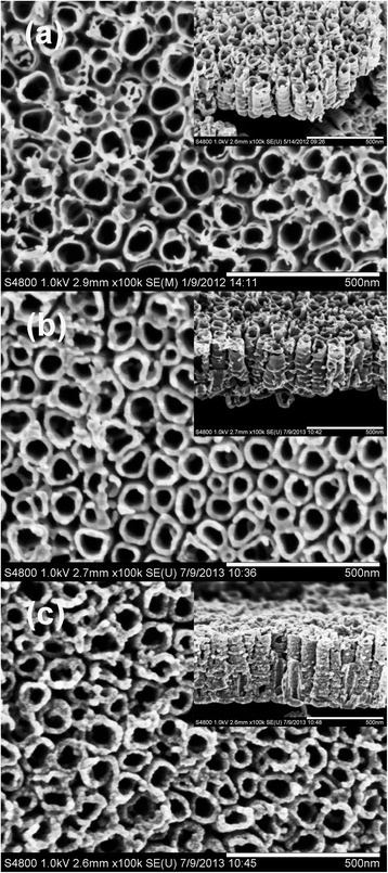
Top-view and cross-sectional SEM images of a bare TiO2 NTs, b 10-cycle ZnO/TiO2 NTs, and c 25-cycle ZnO/TiO2 NTs
Figure 2a shows the random RBS spectra of the bare TiO2 NTs and the ZnO-coated TiO2 NTs. Due to the nanosized tubular structure of the samples, the signals from the scattered helium atoms have no clear and steep edges. The signals attributed to O atoms in the samples are weak, and the resolution is limited by the overlap of its peaks on the base spectra of the heavy element Ti in the underlying Ti foil. The presence of TiO2 NTs on Ti foil can be evidenced by the decreasing of the Ti signal near the Ti background edge. The salient peaks in the channel number ranging from 390 to 430 in the spectra of the ZnO-coated TiO2 NTs are related to the contribution from Zn atoms in the ZnO coatings covering the TiO2 NTs. The coverage of the TiO2 NTs by ZnO coatings also results in further decreasing of the Ti signal near the Ti background edge. In comparison to the spectrum of the 10-cycle ZnO/TiO2 NTs, the higher yield attributed to Zn in the spectrum of the 25-cycle ZnO/TiO2 NTs indicates the thicker ZnO coating of the 25-cycle ZnO/TiO2 NTs. However, the thickness and the composition of the ZnO coatings cannot be calculated from the spectra shown in Fig. 2a because of the complicated profiles of the spectra taken from the nanosized tubular-structured samples. RBS analysis was also carried out on a ZnO film grown on a polished Si (100) substrate by ALD with 50-cycle deposit of ZnO with the other conditions remaining the same as for depositing ZnO coatings on the TiO2 NTs. The RBS spectrum recorded for the ZnO film on Si is shown in Fig. 2b. The SIMNRA simulation [25] of this spectrum reveals that the ZnO film has a stoichiometric composition and a thickness of 10.25 nm, from which it is deduced that the thickness of 1-cycle deposit of ZnO is about 0.21 nm, consistent with the result obtained by spectroscopic ellipsometry performed for a ZnO thin film on a Si substrate deposited by the same method and conditions, which gave an estimated thickness of 0.225 nm for 1-cycle deposit of ZnO [26]. Therefore, the 10-cycle ZnO/TiO2 NTs and 25-cycle ZnO/TiO2 NTs can be estimated to have a ZnO coating of about 2.10 and 5.25 nm in thickness, respectively.
Fig. 2.
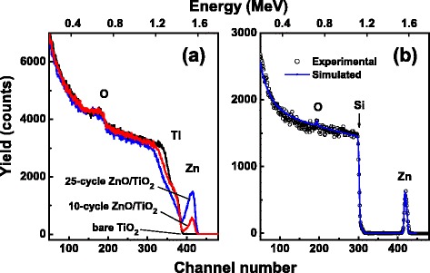
a RBS spectra of bare TiO2 NTs, 10-cycle ZnO/TiO2 NTs, and 25-cycle ZnO/TiO2 NTs. b Experimental (circle) and simulated (solid line) RBS spectra of a ZnO film grown on a Si substrate by ALD with 50-cycle deposit of ZnO
Figure 3a illustrates the XRD patterns of the bare TiO2 NTs and the TiO2 NTs covered by ZnO coatings. Besides the diffractions from the Ti foil (denoted by T), a prominent diffraction peak with 2θ at 25.22 is identified for the samples whether covered by ZnO or not. This peak is indexed to the (101) diffraction of anatase TiO2 (denoted by A in Fig. 3a) (JCPDS 21-1272). For the bare TiO2 NTs, in addition, a weak peak near 27.40 can be recognized, which could be assigned to the (110) diffraction of rutile TiO2 (denoted by R) (JCPDS 21-1276). The TiO2 NTs are therefore of nearly tetragonal anatase phase with minor rutile phase. For the TiO2 NTs covered by a 10-cycle deposit of ZnO, three additional peaks appear, which can be ascribed to hexagonal wurtzite ZnO (denoted by W) and are related to the diffractions from the (100), (002), and (101) orientations of wurtzite ZnO (JCPDS: 36-1451), respectively. The multidiffractions reveal the non-oriented growth of ZnO on the TiO2 NTs. For the TiO2 NTs covered by a 25-cycle deposit of ZnO coating, the diffractions ascribed to wurtzite ZnO increase with a reduced peak width, indicating an improvement in the crystallinity of the ZnO coating with the coating thickness increasing. The above XRD results reveal that fabricated ZnO/TiO2 NTs are constructed of tetragonal anatase TiO2 NTs and hexagonal wurtzite ZnO coatings.
Fig. 3.
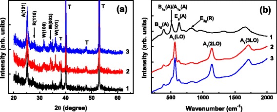
a XRD patterns and b Raman scattering spectra of bare TiO2 NTs (1), 10-cycle ZnO/TiO2 NTs (2), and 25-cycle (3) ZnO/TiO2 NTs. The XRD patterns and Raman scattering spectra are moved vertically for clarity
Raman backscattering measurements confirm the anatase structure of the TiO2 NTs and the wurtzite structure of the ZnO coatings, as shown in Fig. 3b. The Raman spectrum taken from the bare TiO2 NTs exhibits three distinct peaks located at 392, 514, and 633 cm−1, respectively. They are attributed to the characteristic Raman reactive B1g mode, doublet A1g/B1g mode, and Eg mode of anatase TiO2 [27, 28]. In addition, a broad band centered near 820 cm−1 is resolved, which is attributed to the B2g mode of rutile TiO2. In the Raman spectrum taken from the bare TiO2 NTs, A and R in parentheses denote the anatase and the rutile phase of TiO2, respectively. After being covered by a 10- or 25-cycle deposit of ZnO coating, the above TiO2 modes are greatly suppressed and the Raman spectra are predominated by three strong backscattering peaks at 574, 1147, and 1720 cm−1. The strongest peak at 574 cm−1 is attributed to the polar optical mode associated with longitudinal optical (LO) phonons of ZnO [A1(LO)], while the other two peaks at 1147 and 1720 cm−1 are the overtones of A1(LO) and result from 2- and 3-phonon scattering processes [A1(2LO) and A1(3LO)], respectively [29, 30]. The reduction in the measured Raman signals scattered from TiO2 for the ZnO-coated TiO2 nanotubes is mainly attributed to the absorption of the photons in the exciting 325-nm light by the ZnO coating.
The morphology of the ZnO/TiO2 NTs and the crystal structure of the TiO2 tubes and the ZnO coatings are further confirmed by TEM and high-resolution TEM examination, as shown in Fig. 4 which depicts representative TEM and high-resolution TEM images taken from the 25-cycle ZnO/TiO2 NTs. The heterogeneous structure can be seen clearly from the images shown in Fig. 4a, b. We have measured the wall thickness of TiO2 tube yielding ~15 nm which is consistent with the result obtained by FESEM, and the thickness of ZnO coating on the inner-wall of TiO2 tube giving ~5 nm, consistent with that estimated by RBS. The high-resolution TEM image evidences the crystal structure of the TiO2 tube and the ZnO coating. The interplanar spacings were determined for both TiO2 and ZnO. We can see from Fig. 4b that TiO2 is nearly single crystalline with interplanar spacing of 0.35 nm which is in agreement with d101 of anatase TiO2. Figure 4b also reveals several orientations of ZnO. Their interplanar spacings were determined to be 0.28, 0.26, and 0.25 nm, respectively, matching well with d100, d002, and d101 of wurtzite ZnO. The crystal structure of the sample characterized by high-resolution TEM is in conformity with the XRD characterization.
Fig. 4.
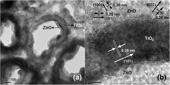
Representative a TEM and b high-resolution TEM images of 25-cycle ZnO/TiO2 NTs
The recorded UV–visible absorption spectra of the samples are displayed in Fig. 5. It can be seen that compared with the bare TiO2 NTs, the ZnO-coated TiO2 NTs exhibit an obvious red shift in the absorption edge, indicating that the ZnO coating on the TiO2 NTs extends the photoresponse to longer wavelength, and the red shift increases with the ZnO coating thickness increasing. The red shift in the absorption edge of heterostructured materials composed of TiO2 and ZnO has been reported and can be attributed to the staggered band gaps of TiO2 and ZnO and the interface effect between TiO2 and ZnO [9, 31, 32]. The red-shifted absorption edge and consequently the extended photoresponse region allow the ZnO-coated TiO2 NTs to work in the visible region.
Fig. 5.
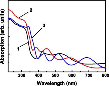
UV–visible absorption spectra of bare TiO2 NTs (1), 10-cycle ZnO/TiO2 NTs (2), and 25-cycle (3) ZnO/TiO2 NTs
Figure 6a shows the PL spectra of the samples measured at 300 K. For the 25-cycle ZnO/TiO2 NTs, an intense UV luminescence peaking at about 376 nm is observed, with very weak visible emission associated with defects such as oxygen vacancies [33, 34]. This UV luminescence is emitted from the ZnO coatings and corresponds to the room-temperature free exciton-related near-band-edge (NBE) emission of ZnO [30, 35, 36]. The intense UV ZnO NBE luminescence and the weak defect-related emission reveal the high quality of the ZnO coating and low concentration of defects. Aside from weak defect-related emission, in contrast, no obvious luminescence can be observed from the bare TiO2 NTs and the TiO2 NTs covered by a 10-cycle deposit of ZnO coating. The former is expected to have low probability of radiative recombination processes due to the indirect band energy structure of TiO2 [37, 38]. For the latter, the light excitation of the ultrathin ZnO coating might be ineffective, and hence, the generation of electrons and holes in the ultrathin ZnO coating is limited due to its ineffective absorption of exciting photons. Additionally, the suppression of electron-hole recombination due to the efficient spatial separation of electrons and holes in the heterostructured ZnO/TiO2 reduces the luminescence from the ZnO coating.
Fig. 6.
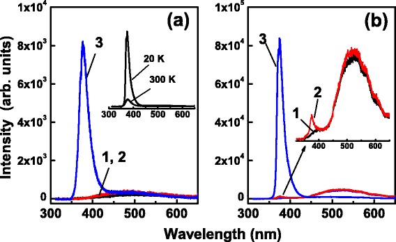
PL spectra of bare TiO2 NTs (1), 10-cycle ZnO/TiO2 NTs (2), and 25-cycle (3) ZnO/TiO2 NTs measured at 300 K (a) and 20 K (b). The inset in a compares the PL spectra of 25-cycle ZnO/TiO2 NTs measured at 300 and 20 K, and the inset in b shows magnified spectra 1 and 2 recorded at 20 K
Generally, the PL from the sample becomes stronger at low temperatures. The inset in Fig. 6a compares the PL spectra of the 25-cycle ZnO/TiO2 NTs measured at 300 and 20 K, respectively. At 20 K, the intensity of the UV ZnO NBE luminescence is increased about one order of magnitude for the 25-cycle ZnO/TiO2 NTs as a result of the freezing of phonons and the quenching of nonradiative recombination processes at low temperatures [30, 35, 39]. The UV ZnO NBE luminescence at low temperature is still without the company of defect-related visible emission, but with a narrowed width as compared to that recorded at room temperature, as shown in Fig. 6b which illustrates the PL spectra recorded at 20 K. For the bare TiO2 NTs, only the defect-related visible emission is observed. In addition to the defect-related visible emission, the PL of the 10-cycle ZnO/TiO2 NTs includes a weak UV NBE luminescence from the ZnO coating with its intensity less than 2 % of that of the 25-cycle ZnO/TiO2 NTs. The comparison of the PL spectra of the ZnO-coated TiO2 NTs with that of the bare TiO2 NTs, measured at room temperature and low temperature, suggests that the visible emission is most probable associated with the defects in TiO2 NTs. Moreover, the much weak PL from the 10-cycle ZnO/TiO2 NTs as compared to that from the 25-cycle ZnO/TiO2 NTs reveals a lower rate of radiative recombination of photogenerated electrons and holes in the 10-cycle deposit of ZnO than in 25-cycle deposit of ZnO, implying that ZnO/TiO2 NTs with a thinner rather than a thicker ZnO coating have more efficient spatial separation of photogenerated electrons and holes and hence exhibit better photoelectrochemical activity as will be described below.
From the typical electrochemical impedance spectroscopy (EIS) Nyquist plots of the bare TiO2 NTs and the heterogeneous structured ZnO-coated TiO2 NTs illustrated in Fig. 7a, we can determine the charge transfer resistance (Rct) of the samples when being used as electrodes. The charge transfer resistance of an electrode is one of the important parameters concerning the kinetics at the electrode. Compared to the bare TiO2 NTs, the TiO2 NTs covered by a 10-cycle deposit of ZnO present a decrease in Rct, as implied by the smaller value of the arc diameter in the Nyquist plot, indicating that the transfer of charges across the interface between the electrode and the solution becomes easier. However, the presence of the 25-cycle deposit of ZnO on the TiO2 NTs results in an increased Rct, even higher than that of the bare TiO2 NTs. The increase in Rct is probably attributed to a longer transport path for charges because of the thicker ZnO coating on the TiO2 NTs and to a higher recombination rate of electrons and holes in the electrode, since the recombination rate in ZnO is higher than that in the TiO2 [40].
Fig. 7.
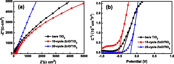
a Nyquist plots and b Mott–Schottky plots of bare TiO2 NTs, 10-cycle ZnO/TiO2 NTs, and 25-cycle ZnO/TiO2 NTs
The flat-band potentials of the TiO2 NTs and ZnO/TiO2 NTs electrodes were determined by the Mott–Schottky analysis method [41, 42]. Figure 7b displays the Mott–Schottky plots of the bare TiO2 NTs and the ZnO-coated TiO2 NTs. The reversed sigmoidal plots with an overall shape are consistent with that typical for n-type semiconductors [42]. In addition, the reproducible flat-band potentials, i.e., the potentials corresponding to the situation in which there is no charge accumulation in the semiconductor so that the energy bands experience no bending can be obtained by intersecting the tangent of Mott–Schottky curves with the potential axis. The flat-band potential (Vfb) for the 10-cycle ZnO-coated TiO2 NTs shifts negatively to −0.53 V from −0.42 V for the bare TiO2 NTs, revealing a smaller barrier for charge transfer in the 10-cycle ZnO/TiO2 NTs. The thin ZnO coating on the TiO2 surface forms an inherent barrier layer to block electron transfer from the conduction band or trap sites of TiO2 to electrolyte, retarding charge recombination in the TiO2/electrolyte interface [43]. The Vfb plays an important role in photoelectrochemical performance. A more negative Vfb suggests a higher photoelectrochemical activity. When used as the photoelectrode in a photovoltaic device, for example, a higher open-circuit voltage can be expected, since the open-circuit voltage (Voc) of a photovoltaic device is generally determined by the offset between the quasi Fermi level of electrodes and the redox level of electrolyte [44]. However, the 25-cycle ZnO-coated TiO2 NTs present a smaller negative value of Vfb, even smaller than that of the bare TiO2 NTs. This can also be attributed to the higher recombination rate in thicker ZnO coating.
Figure 8 shows the cyclic voltammetry curves obtained for the bare TiO2 and the ZnO-coated TiO2 NTs electrodes in the 0.5 M Na2SO4 solution at a scan rate of 50 mV/s. All the cyclic voltammograms show hysteretic shape characteristics, which suggests that electron charging/discharging occurs in the electrode/electrolyte interface, forming Faradic currents in the electrolyte. Moreover, the ZnO coating on TiO2 induces a shift in the on-set potential of the cathodic current, consistent with the shift of flat-band potential, revealing that the ZnO coating plays a role as a blocking layer suppressing electron flow to the electrolyte. The shift of the on-set potential is also attributed to the changes of the interface states or traps on TiO2 surface covered by the ZnO coating.
Fig. 8.
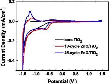
Cyclic voltammograms of bare TiO2 NTs, 10-cycle ZnO/TiO2 NTs, and 25-cycle ZnO/TiO2 NTs in a 0.5 M Na2SO4 solution at a scan rate of 50 mV/s
Figure 9a illustrates the transient photocurrent responses of the ZnO-coated TiO2 NTs used as photoelectrodes under intermittent illumination by light with a wavelength cutoff of 380 nm and compares with that of the bare TiO2 NTs photoelectrode. Whether covered by a ZnO coating or not, the PC densities of the photoelectrode have a transient increase when the light on the electrode is turned on and decrease nearly to zero as soon as the incident light is turned off, demonstrating that the samples have a fast photoresponse speed and reasonably good photostability when used as photoelectrodes. Obviously, the coverage of the TiO2 NTs by ZnO coatings results in an increase in PC density and hence an enhancement in photoelectrochemical activity compared with the uncovered TiO2 NTs, and it seems that the increase of PC density and the enhancement of photoelectrochemical activity are nearly the same for the TiO2 NTs covered by a 10- or 25-cycle deposit of ZnO coating. The increased PC density and the enhanced photoelectrochemical activity of the ZnO-coated TiO2 NTs can be attributed to the nanotube-shaped TiO2 structure which has a large effective surface area in close proximity with the ZnO coating and consequently results in an increase of diffusive transport of photogenerated electrons and holes. In the heterogeneous structure composed of anatase TiO2 and wurtzite ZnO, in addition, an efficient spatial separation of photogenerated electrons and holes is expected, which also contributes to the increased PC density and the enhanced photoelectrochemical activity.
Fig. 9.
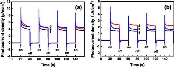
Transient PC densities of bare TiO2 NTs (1), 10-cycle ZnO/TiO2 NTs (2), and 25-cycle (3) ZnO/TiO2 NTs under illumination of light with wavelength cutoffs of 380 nm (a) and 420 nm (b)
The enhanced photoelectrochemical activity of the ZnO-coated TiO2 NTs can be better understood based on the staggered band alignment for the ZnO-coated TiO2 NTs on Ti foil as delineated in Fig. 10. Although the band gap energies of ZnO and TiO2 are similar (~3.37 vs ~3.22 eV), both the conduction band minimum (CBM) and valence band maximum (VBM) of ZnO lie a little above those of TiO2 [45], making a type-II heterojunction with a work function of about 5.2 eV for ZnO [46] and that of about 5.1 eV for TiO2 [47]. The contact between TiO2 and the underlying Ti foil is ohmic by nature, as the work function of Ti (4.33 eV) is less than that of TiO2. Therefore, when the nanoheterostructure is subjected to a positive bias, the electrons of the CB of ZnO can easily enter into the CB of TiO2 and then collected by the metallic Ti foil, whereas the holes of the VB of TiO2 can easily enter into the VB of ZnO. With excitation under light illumination, the photogenerated electrons in both TiO2 and ZnO reach at the interface between TiO2 and the Ti foil and are collected by the Ti foil, whereas the photogenerated holes reach at the ZnO surface where charge transfers occur between the electrolyte and the ZnO surface via electrochemical reactions.
Fig. 10.
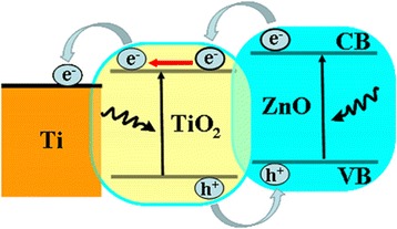
Band alignment of ZnO/TiO2 NTs grown on metallic Ti foil with schematic illustration for charge separation and transfer under illumination of light
The increased PC density and the enhanced photoelectrochemical activity can also be ascribed to a large number of electron-hole pairs formed under the illumination of the light around 380 nm the energy of whose photons is nearly resonant with the band gap of ZnO. As described above, however, the presence of the ZnO coatings on the TiO2 NTs results in a red shift of absorption edge and allows the ZnO-coated TiO2 NTs to absorb visible light. In order to investigate the influence of the ZnO coverage on the photoelectrochemical activity under visible illumination, PC measurements were also performed under intermittent visible illumination with a wavelength cutoff of 420 nm. Although the corresponding PC densities are generally lower than those obtained under the illumination with the wavelength cutoff of 380 nm, the ZnO-covered TiO2 NTs present enhanced photoelectrochemical activities compared with the bare TiO2 NTs. For the 10-cycle ZnO-covered TiO2 NTs, in particular, a significant enhancement of photoelectrochemical activity is observed. The PC density increases from ~1.4 μA/cm2 for the bare TiO2 NTs to ~2.2 μA/cm2 for the 10-cycle ZnO/TiO2 NTs, as shown in Fig. 9b. An increase of nearly 60 % in photoelectrochemical activity is therefore obtained for the TiO2 NTs covered by a 10-cycle deposit of ZnO, or by a 2.1-nm ZnO coating, compared with the bare TiO2 NTs. In contrast, the 25-cycle ZnO/TiO2 NTs just show a slight increase of PC density compared with the bare TiO2 NTs. One of the factors unfavorable for the enhancement in the photoelectrochemical activity of the 25-cycle ZnO/TiO2 NTs should be the thicker ZnO coating, which presents a longer pathway for the generated electrons to migrate to the TiO2 surface and the generated holes to the ZnO surface, and hence increases the recombination of electrons and holes, not conducive to the separation of electrons and holes. Apparently, the higher photoelectrochemical activity of the 10-cycle ZnO/TiO2 NTs is consistent with the suppressed recombination of electrons and holes in the heterogeneous nanostructures composed of TiO2 NTs and ultrathin ZnO coating. The above results suggest that from the view of enhancing photoelectrochemical activity, ZnO coatings of about 2 nm in thickness are optimal for heterostructured ZnO/TiO2 NTs [19, 40, 48, 49].
The bare TiO2 NTs and ZnO-coated TiO2 NTs show good stability in the photoelectrochemical properties. As an example, Fig. 11 shows the PC density of the 10-cycle ZnO/TiO2 NTs for a longtime visible illumination. It is noted that no noticeable change is observed in the PC density after about one and a half hours of visible illumination of light with a wavelength cutoff of 420 nm and the 10-cycle ZnO/TiO2 NTs photoelectrode still presents prompt and excellent transient photocurrent responses under intermittent illumination. It has been reported that unlike ZnO films, ZnO/TiO2 NTs are stable in chemical properties and show excellent photostability [45].
Fig. 11.
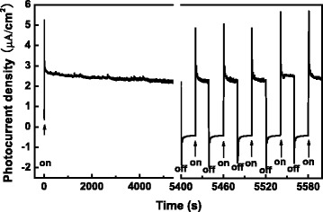
Transient PC density of 10-cycle ZnO/TiO2 NTs under visible illumination with wavelength cutoffs of 420 nm after a longtime illumination
Conclusions
Vertically aligned ZnO-coated TiO2 NTs were fabricated by ALD deposition of ultrathin ZnO coatings on the walls of the TiO2 NTs formed by electrochemical anodization of Ti foils. The TiO2 NTs exhibit anatase structure while the ZnO coatings are structured with hexagonal wurtzite with precise thickness control at atomic scale for an investigation on the influence of ZnO coating and its thickness on the optical, electrochemical, and photoelectrochemical properties of the heterogeneous nanostructured ZnO/TiO2 NTs. The fabricated bare TiO2 NTs and the ZnO-coated TiO2 NTs present fast photoresponse and good photostability. Compared with bare TiO2 NTs, the presence of ZnO coatings significantly improves the electrochemical and photoelectrochemical activities due to the enhanced charge separation in the heterostructure composed of TiO2 NTs and ZnO coatings, especially the TiO2 NTs covered by a thinner ZnO coating of about 2 nm in thickness rather than a thicker ZnO coating. In comparison to the bare TiO2 NTs, an increase of nearly 60 % in photoelectrochemical activity is obtained for the TiO2 NTs covered by an about 2-nm-thick ZnO coating under visible illumination with a wavelength cutoff of 420 nm.
Acknowledgements
This work is supported by the National Natural Science Foundation of China (11275051). Acknowledgment is also made to the Municipal Natural Science Foundation of Shanghai (15ZR1403300).
Footnotes
Competing interests
The authors declare that they have no competing interests.
Authors’ contributions
HC prepared the samples, carried out the experiments, and drafted the manuscript. PL and XY participated in the experiments and manuscript writing. ZH and LS contributed to the result analysis and mechanism discussion. JS and NX characterized the sample structure and studied the optical and photoelectrochemical properties. JW conceived the research and revised the manuscript. All authors read and approved the final manuscript.
References
- 1.Khan SUM, Al-Shahry M, Ingler WB. Efficient photochemical water splitting by a chemically modified n-TiO2. Science. 2002;297:2243–5. doi: 10.1126/science.1075035. [DOI] [PubMed] [Google Scholar]
- 2.Mor GK, Shankar K, Paulose M, Varghese OK, Grimes CA. Use of highly-ordered TiO2 nanotube arrays in dye-sensitized solar cells. Nano Lett. 2006;6:215–8. doi: 10.1021/nl052099j. [DOI] [PubMed] [Google Scholar]
- 3.Rensmo H, Keis K, Lindstroem H, Sodergren S, Solbrand A, Hagfeldt A, Lindquist SE, Wang LN, Muhammed M. High light-to-energy conversion efficiencies for solar cells based on nanostructured ZnO electrodes. J Phys Chem B. 1997;101:2598–601. doi: 10.1021/jp962918b. [DOI] [Google Scholar]
- 4.Zhang QF, Dandeneau CS, Zhou XY, Cao GZ. ZnO nanostructures for dye-sensitized solar cells. Adv Mater. 2009;1:4087–108. doi: 10.1002/adma.200803827. [DOI] [Google Scholar]
- 5.Law M, Greene LE, Johnson JC, Saykally R, Yang PD. Nanowire dye-sensitized solar cells. Nat Mater. 2005;4:455–9. doi: 10.1038/nmat1387. [DOI] [PubMed] [Google Scholar]
- 6.Susmitha K, Kumar MN, Rajkumar G, Giribabu L, Raghavender M. Enhanced dye sensitized solar cell performance with high surface area thin ZnO film and PEDOT:PSS. Sol Energy. 2015;118:126–33. doi: 10.1016/j.solener.2015.03.054. [DOI] [Google Scholar]
- 7.van Embden J, Jasieniak J, Gomez DE, Mulvaney P, Giersig M. Review of the synthetic chemistry involved in the production of core/shell semiconductor nanocrystals. J Chem. 2007;60:457–71. [Google Scholar]
- 8.Roh SJ, Mane RS, Min SK, Lee WJ, Lokhande CD, Han SH. Achievement of 4.51 % conversion efficiency using ZnO recombination barrier layer in TiO2 based dye-sensitized solar cells. Appl Phys Lett. 2006;89:253512. doi: 10.1063/1.2410240. [DOI] [Google Scholar]
- 9.Reiss P, Protiere M, Li L. Core/shell semiconductor nanocrystals. Small. 2009;5:154–68. doi: 10.1002/smll.200800841. [DOI] [PubMed] [Google Scholar]
- 10.Wu ZM, Zhang Y, Zheng JJ, Lin XG, Chen XH, Huang BW, Wang HQ, Huang K, Li SP, Kang JY. An all-inorganic type-II heterojunction array with nearly full solar spectral response based on ZnO/ZnSe core/shell nanowires. J Mater Chem. 2011;21:6020–6. doi: 10.1039/c0jm03971c. [DOI] [Google Scholar]
- 11.Pan L, Shen GQ, Zhang JW, Wei XC, Wang L, Zou JJ, Zhang XW. TiO2-ZnO composite sphere decorated with ZnO clusters for effective charge isolation in photocatalysis. Ind Eng Chem Res. 2015;54:7226–32. doi: 10.1021/acs.iecr.5b01471. [DOI] [Google Scholar]
- 12.Kayaci F, Vempati S, Ozgit-Akgun C, Donmez I, Biyikli N, Uyar T. Selective isolation of the electron or hole in photocatalysis: selective isolation of the electron or hole in photocatalysis: ZnO–TiO2 and TiO2–ZnO core–shell structured heterojunction nanofibers via electrospinning and atomic layer deposition. Nanoscale. 2014;6:5735–45. doi: 10.1039/c3nr06665g. [DOI] [PubMed] [Google Scholar]
- 13.Ji IA, Park MJ, Jung JY, Choi MJ, Lee YW, Lee JH, Bang JH. One-dimensional core/shell structured TiO2/ZnO heterojunction for improved photoelectrochemical performance. Bull Korean Chem Soc. 2012;33:2200–6. doi: 10.5012/bkcs.2012.33.7.2200. [DOI] [Google Scholar]
- 14.Momeni MM, Ghayeb Y. Visible light-driven photoelectrochemical water splitting on ZnO-TiO heterogeneous nanotube photoanodes. J Appl Electrochem. 2015;45:557–566. doi: 10.1007/s10800-015-0836-x. [DOI] [Google Scholar]
- 15.Amna T, Hassan MS, Khil MS, Lee HK, Hwang IH. Electrospun nanofibers of ZnO-TiO2 hybrid: characterization and potential as an extracellular scaffold for supporting myoblasts. Surf Interface Anal. 2014;46:72–6. doi: 10.1002/sia.5350. [DOI] [Google Scholar]
- 16.Liu R, Yang WD, Qiang LS, Liu HY. Conveniently fabricated heterojunction ZnO/TiO2 electrodes using TiO2 nanotube arrays for dye-sensitized solar cells. J Power Sources. 2012;22:153–9. doi: 10.1016/j.jpowsour.2012.07.097. [DOI] [Google Scholar]
- 17.Panigrahi S, Basak D. Core-shell TiO2@ZnO nanorods for efficient ultraviolet photodetection. Nanoscale. 2011;3:2336–41. doi: 10.1039/c1nr10064e. [DOI] [PubMed] [Google Scholar]
- 18.Ulusoy TG, Ghobadiac A, Okyay AK. Surface engineered angstrom thick ZnO-sheathed TiO2 nanowires as photoanodes for performance enhanced dye-sensitized solar cells. J Mater Chem A. 2014;2:16867–76. doi: 10.1039/C4TA03445G. [DOI] [Google Scholar]
- 19.Shaheen BS, Salem HG, El-Sayed MA, Allam NK. Thermal/electrochemical growth and characterization of one-dimensional ZnO/TiO2 hybrid nanoelectrodes for solar fuel production. J Phys Chem C. 2013;117:18502–9. doi: 10.1021/jp405515v. [DOI] [Google Scholar]
- 20.Jeong JS, Choe BH, Lee JH, Lee JJ, Choi WY. ZnO-coated TiO2 nanotube arrays for a photoelectrode in dye-sensitized solar cells. J Electron Mater. 2014;43:375–80. doi: 10.1007/s11664-013-2908-1. [DOI] [Google Scholar]
- 21.Cai H, Yang Q, Hu ZG, Duan ZH, You QH, Sun J, Xu N, Wu JD. Enhanced photoelectrochemical activity of vertically aligned ZnO-coated TiO2 nanotubes. Appl Phys Lett. 2014;104:053114. doi: 10.1063/1.4863852. [DOI] [Google Scholar]
- 22.Cai H, You QH, Hu ZG, Duan ZH, Cui Y, Sun J, Xu N, Wu JD. Fabrication and correlation between photoluminescence and photoelectrochemical properties of vertically aligned ZnO coated TiO2 nanotube array. Sol Energy Mater Sol Cells. 2014;123:233–8. doi: 10.1016/j.solmat.2014.01.033. [DOI] [Google Scholar]
- 23.Ott AW, Chang RPH. Atomic layer-controlled growth of transparent conducting ZnO on plastic substrates. Mater Chem Phys. 1999;58:132–8. doi: 10.1016/S0254-0584(98)00264-8. [DOI] [Google Scholar]
- 24.Zhao JQ, Wang Y. Ultrathin surface coatings for improved electrochemical performance of lithium ion battery electrodes at elevated temperature. J Phys Chem C. 2012;116:11867–76. doi: 10.1021/jp3010629. [DOI] [Google Scholar]
- 25.Mayer M. SIMNRA user’s guide. Garching: Max-Planck-Institut für Plasmaphysik; 1997. [Google Scholar]
- 26.Geng Y, Guo L, Xu SS, Sun QQ, Ding SJ, Lu HL, Zhang DW. Influence of Al doping on the properties of ZnO thin films grown by atomic layer deposition. J Phys Chem C. 2011;115:12317–21. doi: 10.1021/jp2023567. [DOI] [Google Scholar]
- 27.Porto SPS, Fleury PA, Damen TC. Raman spectra of TiO2, MgF2, ZnF2, FeF2, and MnF2. Phys Rev. 1967;154:522–4. doi: 10.1103/PhysRev.154.522. [DOI] [Google Scholar]
- 28.Ohsaka T, Izumi F, Fujiki Y. Raman spectrum of anatase TiO2. J Raman Spectrosc. 1978;7:321–4. doi: 10.1002/jrs.1250070606. [DOI] [Google Scholar]
- 29.Scott JF. UV resonant Raman scattering in ZnO. Phys Rev B. 1970;2:1209–11. doi: 10.1103/PhysRevB.2.1209. [DOI] [Google Scholar]
- 30.Li Q, Gao K, Hu ZG, Yu WL, Xu N, Sun J, Wu JD. Photoluminescence and lasing properties of catalyst-free ZnO nanorod arrays fabricated by pulsed laser deposition. J Phys Chem C. 2012;116:2330–5. doi: 10.1021/jp210377s. [DOI] [Google Scholar]
- 31.Hernandez S, Cauda V, Chiodoni A, Dallorto S, Sacco A, Hidalgo D, Celasco E, Pirri CF. Optimization of 1D ZnO@TiO2 core-shell nanostructures for enhanced photoelectrochemical water splitting under solar light illumination. ACS Appl Mater Interfaces. 2014;6:12153–67. doi: 10.1021/am501379m. [DOI] [PubMed] [Google Scholar]
- 32.Yan XD, Zou CW, Gao XD, Gao W. ZnO/TiO2 core–brush nanostructure: processing, microstructure and enhanced photocatalytic activity. J Mater Chem. 2012;22:5629–40. doi: 10.1039/c2jm15477c. [DOI] [Google Scholar]
- 33.Vanheusden K, Warren WL, Seager CH, Tallant DK, Voigt JA, Gnade BE. Mechanisms behind green photoluminescence in ZnO phosphor powders. J Appl Phys. 1996;79:7983–9. doi: 10.1063/1.362349. [DOI] [Google Scholar]
- 34.Li D, Leung YH, Djurisic AB, Liu ZT, Xie MH, Shi SL, Xu SJ, Chan WK. Different origins of visible luminescence in ZnO nanostructures fabricated by the chemical and evaporation methods. Appl Phys Lett. 2004;85:1601–3. doi: 10.1063/1.1786375. [DOI] [Google Scholar]
- 35.Shan W, Walukiewicz W, Ager JW, III, Yu KM, Yuan HB, Xin HP, Cantwell G, Song JJ. Nature of room-temperature photoluminescence in ZnO. Appl Phys Lett. 2005;86:191911. doi: 10.1063/1.1923757. [DOI] [Google Scholar]
- 36.Zhang BP, Binh NT, Segawa Y, Wakatsuki K, Usami N. Optical properties of ZnO rods formed by metalorganic chemical vapor deposition. Appl Phys Lett. 2003;83:1635–7. doi: 10.1063/1.1605803. [DOI] [Google Scholar]
- 37.Chang YH, Liu CM, Chen C, Cheng HE. The effect of geometric structure on photoluminescence characteristics of 1-D TiO2 nanotubes and 2-D TiO2 films fabricated by atomic layer deposition. J Electrochem Soc. 2012;159:D401–5. doi: 10.1149/2.004207jes. [DOI] [Google Scholar]
- 38.Zhang JF, Zhou P, Liu JJ, Yu JG. New understanding of the difference of photocatalytic activity among anatase, rutile and brookite TiO2. Phys Chem Chem Phys. 2014;16:20382–6. doi: 10.1039/C4CP02201G. [DOI] [PubMed] [Google Scholar]
- 39.Ko HJ, Chen YF, Zhu Z, Yao T, Kobayashi I, Uchiki H. Photoluminescence properties of ZnO epilayers grown on CaF2(111) by plasma assisted molecular beam epitaxy. Appl Phys Lett. 2000;76:1905–7. doi: 10.1063/1.126207. [DOI] [Google Scholar]
- 40.Chandiran AK, Abdi-Jalebi M, Nazeeruddin MK, Grätze M. Analysis of electron transfer properties of ZnO and TiO2 photoanodes for dye-sensitized solar cells. ACS Nano. 2014;8:2261–8. doi: 10.1021/nn405535j. [DOI] [PubMed] [Google Scholar]
- 41.Cardon F, Gomes WP. On the determination of the flat-band potential of a semiconductor in contact with a metal or an electrolyte from the Mott-Schottky plot. J Phys D Appl Phys. 1978;11:L63–7. doi: 10.1088/0022-3727/11/4/003. [DOI] [Google Scholar]
- 42.Seungho S, Jang JW, Park YB, Kim JY, Magesh G, Kim JH, Seol M, Yong K, Lee KH, Lee JS. An exceptionally facile method to produce layered double hydroxides on a conducting substrate and their application for solar water splitting without an external bias. Energy Environ Sci. 2014;7:2301–7. doi: 10.1039/c3ee43965h. [DOI] [Google Scholar]
- 43.Kang SH, Kim JY, Kim Y, Kim HS, Sung YE. Surface modification of stretched TiO2 nanotubes for solid-state dye-sensitized solar cells. J Phys Chem C. 2007;111:9614–23. doi: 10.1021/jp071504n. [DOI] [Google Scholar]
- 44.Wu DP, Gao ZY, Xu F, Shi ZP, Tao WG, Jiang K. Nanosheet-based hierarchical ZnO structure decorated with TiO2 particles for enhanced performance in dye-sensitized solar cell. Cryst Eng Comm. 2012;14:7934–41. doi: 10.1039/c2ce25356a. [DOI] [Google Scholar]
- 45.Xiao FX. Construction of highly ordered ZnO–TiO2 nanotube arrays (ZnO/TNTs) heterostructure for photocatalytic application. ACS Appl Mater Interfaces. 2012;4:7055–63. doi: 10.1021/am302462d. [DOI] [PubMed] [Google Scholar]
- 46.Bai XD, Wang EG, Gao PX, Wang ZL. Measuring the work function at a nanobelt tip and at a nanoparticle surface. Nano Lett. 2003;3:1147–50. doi: 10.1021/nl034342p. [DOI] [Google Scholar]
- 47.Xiong G, Shao R, Droubay TC, Joly AG, Beck KM, Chambers SA, Hess WP. Photoemission electron microscopy of TiO2 anatase films embedded with rutile nanocrystals. Adv Funct Mater. 2007;17:2133–8. doi: 10.1002/adfm.200700146. [DOI] [Google Scholar]
- 48.Cheun H, Fuentes-Hernandez C, Zhou YH, Potscavage WJ, Kim SJ, Shim J, Dindar A, Kippelen B. Electrical and optical properties of ZnO processed by atomic layer deposition in inverted polymer solar cells. J Phys Chem C. 2010;114:20713–8. doi: 10.1021/jp106641j. [DOI] [Google Scholar]
- 49.Greene LE, Law M, Yuhas BD, Yang PD. ZnO-TiO2 core-shell nanorod/P3HT solar cells. J Phys Chem C. 2007;111:18451–6. doi: 10.1021/jp077593l. [DOI] [Google Scholar]


