Abstract
Three-dimensional nanostructures combine properties of nanoscale materials with the advantages of being macro-sized pieces when the time comes to manipulate, measure their properties, or make a device. However, the amount of compounds with the ability to self-organize in ordered three-dimensional nanostructures is limited. Therefore, template-based fabrication strategies become the key approach towards three-dimensional nanostructures. Here we report the simple fabrication of a template based on anodic aluminum oxide, having a well-defined, ordered, tunable, homogeneous 3D nanotubular network in the sub 100 nm range. The three-dimensional templates are then employed to achieve three-dimensional, ordered nanowire-networks in Bi2Te3 and polystyrene. Lastly, we demonstrate the photonic crystal behavior of both the template and the polystyrene three-dimensional nanostructure. Our approach may establish the foundations for future high-throughput, cheap, photonic materials and devices made of simple commodity plastics, metals, and semiconductors.
Introduction
Applications of nanomaterials would be undoubtedly ubiquitous, including areas from everyday life to the most advanced science, as they often present new or enhanced properties ascribed to their low dimensionality.1 However, the practical employment of these nano-sized components into a macro-scale device, which must be manufactured in a factory, manipulated by an operator and used in a macro-scale world, is frequently hard to carry out. Therefore, the development of high-throughput nanotechnologies for real life applications has been hitherto relatively slow. A promising strategy toward this goal is to integrate the nano-sized components into a large, hierarchical structure up to the macro-scale. Such a material would behave according to the properties of its individual nanocomponents –thus, low dimensionality effects are expected-while being a macroscale-size piece and, hence, easy to be manipulated and used. 3D nanowire-like networks, having a hierarchical architecture comprised of orderly interconnected nanowires, are a good example of these kinds of materials. In fact, they are demonstrating enhanced properties for many applications, as sensors,2, 3 electrochromic devices,4, 5 solar cells,6, 7 energy storage,8, 9, 10 scaffolds with special mechanical properties, 11 optical elements,12, 13 and for electrocatalysis.14 Hence, it exists a pressing need for three-dimensional nanofabricated structures.
Nevertheless, despite of the well-recognized potential of these kinds of 3D nanostructures, their use has been hitherto scarce due to the lacks of scalable methods to synthesize/process functional materials of the desired characteristics. For example, the macroscopic extension of 3D-periodic nanostructures restricts their fabrication approaches to those compatible with an affordable large-area production. Therefore, bottom-up fabrication strategies, which exploit the self-organization of building blocks, turn out to be the most appropriate approaches. Unfortunately, the amount of compounds which have the ability to self-organize in 3D periodic structures is limited,15 which avoids the direct employment of this approach for most of functional materials. A promising alternative method for periodic 3D nanowire-like networks composed of those materials that do not present self-organizing capabilities is the use of appropriate templates. These templates must present, on the one hand, the inverse morphology of the target nanostructure, i.e. a 3D nanotubular network, and, on the other hand, a macroscopic extension. Thus, currently, the main challenge in the fabrication of 3D-periodic nanowire-like networks is the development of versatile templates with periodic (ordered) 3D nanotubular networks.
Gyroid forming block copolymers –with sacrificial continuous domains-have recently demonstrated to be efficient platforms to integrate 3D templates for the preparation of 3D nanostructures in Au,12 NiO,5 V2O5 10, TiO2,16 by electrodeposition or sol-gel reactions. Likewise, 3D Pt nanowire networks have been also produced by electrodeposition within a track-etched polymer 3D membrane.14. Both kinds of polymer templates have shown their suitability for the growth of inorganic compounds by non-aggressive, wet-chemical approaches. However, growth methods yielding inorganic materials with the best compositional and crystallographic features -which will eventually present the best properties-, such as, atomic layer deposition, molecular beam epitaxy, chemical vapor deposition, and the like, commonly imply/need aggressive reaction conditions namely, high temperatures, high vacuum, or presence of highly reactive species, which are hardly supported by polymer templates. Thus, block copolymer templates and most of track-etched templates are not compatible with many of these growth techniques, which avoids the nanostructuration of an important set of inorganic materials by this approach. Note that gyroid 3D nanotubular network structures are frequently conformed in polymers as polystyrene, poly(ethyleneoxide), etc., which present a working temperature below 100 °C. Furthermore, the low surface energy of polymeric templates (γpolymers < 50 mN/m) might hinder the infiltration of other low surface energy liquid compounds, such as most of organic liquids -polymer solutions and melts, liquid crystals, and the like-, into the tubular space. This would prevent to make 3D-nanowire-like networks composed of many functional organic materials.
In this work, we present the fabrication of a well-defined, controllable, homogeneous periodic 3D nanotubular network over cm2 areas in anodic aluminum oxide (AAO), with tens of micron thickness and high aspect-ratio. The produced template is composed of alumina, so it is mechanically, chemically and thermally stable and possesses high-surface-energy hydroxilated pore walls, which may promote the infiltration of low surface energy fluids. The 3D-AAO presented here consists of a hexagonal array of longitudinal nanopores, which are perpendicularly interconnected through transversal nanochannels. Thus, it constitutes a perfectly ordered 3D nanoarchitecture in porous alumina, in contrast to other analogous materials previously reported.17, 18, 19 Such transversal nanochannels form thus networks confined into planes parallel to the alumina surface. The used fabrication approach is inspired on the “potentiostatic pulsed anodization” developed by Lee et al.,20, 21 in which mild anodization (MA) and hard anodization (HA) steps are alternated.20, 22, 23 However, in our approach, during HA steps the current is limited to a defined value. Then, we take advantage of the higher etching rates of the aluminum oxide grown under HA20 to attack selectively those regions, in such a way that longitudinal nanopores become interconnected with their first neighbourgs through transversal nanochannels. The amount and position of the pore-interconnecting-junctions of the tubular network can be precisely adjusted just by selecting the amount and the length of the MA steps. Due to the adjustable, dense and ordered 3D-nanoporous structure, the 3D-AAOs presented here can be used as templates for the fabrication of 3D periodic nanowire-like networks in a wide variety of materials with applications in thermoelectricity24, catalysis25, filtration,26 energy storage,10 and photonics,2 to name some. Moreover, we show here our results on the fabrication of 3D-nanowire-like periodic nanostructures using 3D-AAO templates. Thereby, 3D-nanowire-like periodic nanostructures made of polystyrene (PS), by in-situ polymerization; and Bi2Te3, by electrodeposition, were fabricated 27, 28, 29 in order to demonstrate the suitability of our templates to fabricate nanowires networks for both organic and inorganic materials using different growth techniques. Lastly, the 1D photonic crystal behaviour of both the 3D AAO and a 3D periodic nanowire-like networks made of a commodity plastic as polystyrene is demonstrated, which opens up the possibility to produce high-throughput, cheap, photonic materials and devices made of simple commodity plastics.
Results
Anodization Processes
During a typical pulse anodization process MA and HA constant voltage steps are periodically alternated.20, 22, 23 However, in our approach while constant voltage is applied in MA steps, the current is limited to a defined value during HA steps and thereof the voltage is not kept constant. The material is grown thus at a defined current during HA periods. Then, the obtained AAO is selectively etched. As a consequence, the aluminum oxide grown under HA is partially removed, so that transversal nanochannels are formed, establishing thus the 3D porous network.
Since our aim is to achieve a periodic 3D structure, the ordering of the longitudinal pore arrangement must not be disturbed as a consequence of the alternation of HA and MA steps. From a practical point of view, this means that the AAO layers grown under MA conditions and under HA must present the same latticing parameter of the hexagonal pore arrangement (Dint,long). Dint,long is proportional to the applied voltage in both MA and HA regimes, but the proportionality coefficient, ζ, is different in each of them. The Dint,long is 65 nm for an AAO grown in MA conditions under a voltage (VMA) of 25 V, so that one should carry out the HA pulses at a voltage leading to the same Dint,long value. According to Schwrim et al.,30 the relationship between Dint,long and the applied voltage in the potentiostatic HA regime is ζHA=1.8 nm/V. Thus, the applied voltage during the pulses should be 36 V. However, we experimentally observe that when applying pulses of 36 V without limiting the current intensity, we are not able to grow 3D-AAO with homogeneous porous structure, as the high current during pulses induced severe damages in the structure –probably due to heating effects. We manage to solve this problem by limiting the intensity during the pulses (IHA) to 55 mA (i.e. a current density, j, of 27.5 mA/cm2). Moreover, the current limitation assures that the kinetics of the reaction during the pulses is almost independent on reaction time, so that the same AAO thickness grows in each pulse (Figure 1a). Note that the amount of material grown is directly proportional to j during anodization.31,32 In contrast, when one directly pulses between constant voltage during MA steps (VMA) and constant voltage during HA pulses, the current at the HA pulses (IHA) decreases with time20 as the pore become longer and, thus, the grown of the AAO turns to be dependent on the anodization time, which leads to a non-homogeneous network structure in the AAO template (see Supplementary Figure 1 and Supplementary Note 1). This issue is avoided by our procedure. Due to the current limitation to 55 mA, the maximum voltage (VHA) reached during the pulses is 31-31.5 V (see Figure 1b), so we fix the nominal applied voltage for the pulses (VHA,N) to 32 V. The length of the pulse (tHA) is established in 2 s, as we observe that the AAO layer grown during such a pulse is the appropriate to afterwards develop transversal nanochannels of the desired dimensions (a few tens of nanometers). Furthermore, we observe that even if we do not anodize exactly at a VHA,N giving rise to a Dint,long of 65 nm, a 2 s pulse is a too short time for the system to lose its order –as will be shown below and in Supplementary Figure 2 (Supplementary Note 2). Hence, a 3D AAO is achieved with a highly regular morphology. On the other side, the length of the MA (tMA) steps is varied to tailor the distance between transversal nanochannels, as it will be shown below.
Figure 1. Pulse anodization.
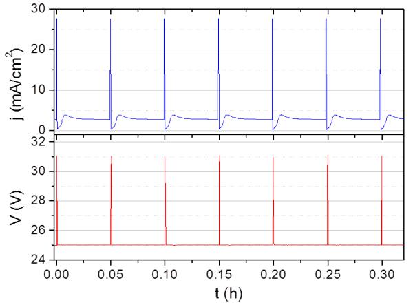
Current-time (a) and voltage-time (b) transients during pulse anodization. Anodization process consists of a periodic alternation of Mild Anodization (MA) steps followed by Hard anodization (HA) steps. The maximum intensity is fixed at 55 mA.
The 3D Anodic Aluminum Oxide Template
Figure 2a shows a representative SEM image of a longitudinal fracture surface of 3D-AAO template fabricated by pulse anodization (VMA=25 V, tMA=100 s; VHA,N=32 V, tHA= 2 s) and subsequent partial chemical etching of the HA regions with H3PO4 5 wt %, at 30 °C, for 18 min. Longitudinal pores laid on the vertical direction, while transversal nanochannel layers are arranged along the horizontal and the out-of-plane directions of the image. Thereby, the 3D nanochannel network in the 3D-AAO consist of a set of parallel longitudinal nanopores, like those formed via a constant voltage anodization process in “common“ AAO templates, and transversal nanochannels, which interconnect adjacent longitudinal nanopores at some periodic points. The tubular network structure is thus similar to that of the illustration in Figure 2b. The MA/HA alternating layer structure of the 3D-AAOs induced the appearance of structural color in the 3D-AAO as both layers have different refracting indexes and are periodically alternated. The 3D-AAO thus behaves as a distributed Bragg reflector (DBR) or a 1D photonic crystal, as can be observed in Figure 2c, in which optical images of the 3D-AAO acquired from different viewing angles are shown. It can be appreciated a change in color while rotation the sample. Such alternating layered structure can be clearly appreciated in the cross-sectional SEM image in Figure 2d.
Figure 2. 3D-Anodic alumina template.
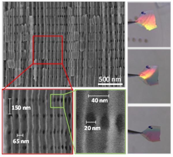
(a) Representative cross-section SEM image of the 3D-AAO template fabricated by pulse anodization (VMA=25 V, tMA=100 s; VHA,N =32 V, tHA= 2 s) and subsequent partial chemical etching of the HA regions with H3PO4 5 wt %, at 30 °C, for 18 min. The sample has being broken to see the cross-section more clearly. Scale bar represents 5 μm. (b) Schematic cartoon of the interconnected nanochannel network structure of the 3D-AAO templates. (c) Optical photographs of a 3D-AAO acquired from different viewing angles (the sample is suspended with tweezers). The arrow indicates the rotation direction. (d) Cross section micrograph of a 3D-AAO template, in which the nanostructure of the template can be appreciated. Scale bar represents 500 nm. (e) Enlarged view of the area marked in (d) with a rectangle, in which both the longitudinal pores (in the vertical direction) and the transversal pores (in the horizontal and in the out-of-plane direction of the image) can be distinguished. The distance between longitudinal nanopores (Dint,long) is 65 nm, while the separation of the planes containing the transversal nanopores (Dint,trans) is 150 nm for this specific 3D-AAO (f) Detailed view of the nanochannel structure from which the dimensions of different nanopores can be measured. The diameter of longitudinal nanopores is 40 nm. The section of the transversal nanochannels is rather ellipsoid, presenting a short diameter of 20 nm and a large diameter of approximately 35 nm.
The dimensions of the structural features of a 3D AAO obtained after 60 MA/HA repetitions (VMA=25 V, tMA=100 s; VHA,N=32 V, tHA= 2 s) and the subsequent etching process in H3PO4 5 wt %, at 30 °C, for 18 min are shown in Figures 2d, 2e, and 2f. The total area of the 3D template is 2. In the direction perpendicular to the template surface, the thickness of the 3D porous structure is ~20 μm (only about 10 μm are shown in Figure 2a), but it can be increased through a higher amount of MA/HA repetitions. Hence, the whole 3D porous network has macroscale dimensions. In contrast, the structure of the network entirely nanoscopic. The distance between longitudinal nanopores (Dint,long) is 65 nm, while the distance between planes containing the transversal nanopores (Dint,trans) is 150 nm for this specific 3D-AAO example (Figure 2e). Longitudinal nanopores present a diameter of 40 nm due to the pore-widening process (originally, 25 nm in diameter pores are obtained), as observed in Figure 2f. In such micrograph longitudinal nanopores lay vertically and the transversal nanochannels lay out-of-plane of the image. The diameter of transversal nanochannels depends on the chemical etching process. For the typical etching process indicated above, the section of the transversal nanochannels is rather ellipsoid, presenting a short diameter of 20 nm and a large diameter of approximately 35 nm (Figure 2f).
Even though the three dimensional porous architecture in 3D-AAOs is a consequence of the pulsed anodization, only one-dimensional longitudinal nanopores are originally formed due to the anodization process, as can be observed in Figure 3a. However, the alumina grown under HA conditions is chemically less stable than that grown under MA conditions, as found by Lee et al 20. Thereby, the chemical etching rate of the alumina grown under HA is significantly higher than of that grown under MA. In this way, when the AAO is attacked with an acid solution, AAO regions formed during the HA pulse are preferentially dissolved. Hence, one may preferentially widen the longitudinal nanopores in the HA regions until each longitudinal pore collapses with the next neighbor, without affecting significantly to the longitudinal nanopore regions formed under MA steps, thus creating transversal nanochannels between longitudinal nanopores (Figure 3b).
Figure 3. Formation of the 3D porous network.
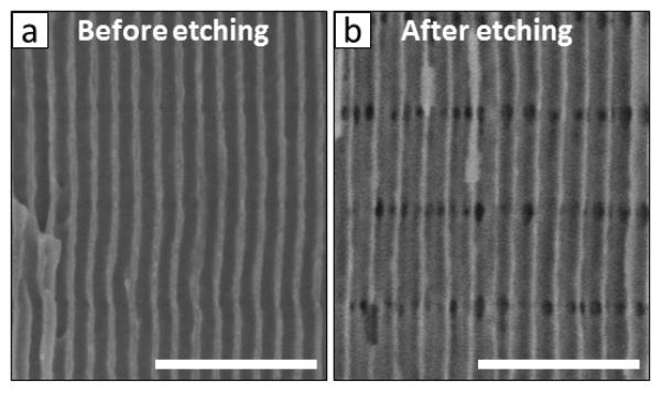
Cross-sectional SEM image of a 3D-AAO prepared by pulsed anodization before (a) and after (b) the chemical etching process in H3PO4 (H3PO4 5 wt %, at 30 °C, for 18 min). Scale bar represents 500 nm.
Geometry of the 3D network
Longitudinal pores are orderly fashioned due to the fact that both the first anodization and the MA steps of the pulse anodization is carried out in self-ordering conditions (25V, 0 °C, 0.3 M H2SO4) (Supplementary Figure 2, Supplementary Note 2). This hexagonal pore distribution is not disturbed by the HA steps, as can be observed in the Supplementary Figure 2c. Therefore, longitudinal nanopores are completely parallel along the entire thickness of the template.
In order to assess the geometry of the transversal nanochannel network, we analyze the morphology of an internal MA terrace after the detachment of the upper layers. A close view of its surface (Figure 4b) reveals that the transversal nanochannels conforms a 2D porous network of hexagonal symmetry (see also Supplementary Figure 3, Supplementary Note 2). This is obviously a consequence of the hexagonal order of the longitudinal nanopore array. Hence, the nanoporous network of the 3D-AAO consists of a hexagonal array of longitudinal nanopores, which are perpendicularly interconnected through the transversal nanochannel network, presenting also hexagonal symmetry (see also (Supplementary Figure 4).
Figure 4. Geometry of transversal nanochannels.
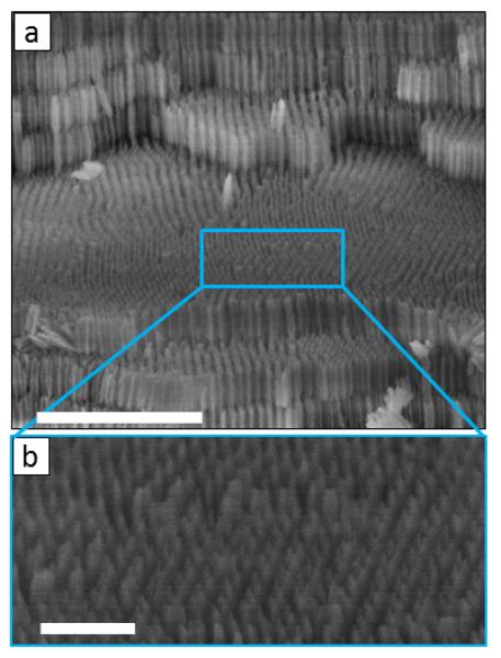
(a) SEM micrograph of a fracture of a 3D-AAO showing a MA terrace after the detachment of the upper layers. Scale bar corresponds to 1μm. And, (b) the transversal nanochannel networks present a hexagonal symmetry as illustrated in the detailed view. Scale bar in this image corresponds to 200 nm It can be observed they are well aligned.
We have tried to extract further information about the HA layer by means of ellipsometry (Supplementary Figures 5 and 6), which gives access to its refractive index and thus can be related to morphological parameters such as the porosity of the layer. For that, a sample is fabricated containing a single transversal nanochannel plane sandwiched between two MA layers, and the ellipsometric data was fixed with a five-layer model that took the fundamental parameters (as described in the Supplementary Note 3). The obtained porosity for the HA layer accounts to 75%.
Tuning geometry of the 3D nanoporous network
In contrast to previous attempts to fabricate 3D structures in AAO, the procedure presented in this work allows a precise control over the morphology of the material. In the approach by Lee et al.17 the spontaneous current oscillations taking place during HA process in oxalic acid electrolyte induced pore diameter modulations, which can be eventually used to prepare a 3D porous network. Nevertheless, although they showed a well-defined 3D porous structure at a local scale, the achieved porous network lacked of structural homogeneity along both the in plane and the cross-plane directions, due to the fact that the formation of the network is consequence of self-induced current oscillations, which are difficult, if not infeasible, to be controlled. Therefore, one cannot adjust the period, the shape, and the amplitude of the diameter modulations by their approach and, in consequence, neither the morphology of the 3D porous network. Furthermore, the AAO template they obtained presented a thickness distribution over the film. Likewise, in Losic’s19, 33 and Wang’s18 approach, the non-perfect organization of longitudinal pores together with lengthy etching treatments required for interconnecting the longitudinal pores lead to severe structural damages in the material. On the contrary, one can precisely adjust the amount and position of the pore-interconnecting-junctions of the tubular network through our approach, just by selecting the amount and the length of the MA regions, as it can be observed in Figure 5. Moreover, since every single step in the anodization processes is well controlled and homogeneous, we can achieve well defined 3D porous structures with no structural defects. Thereby, we fabricate 3D-AAOs having different distances between transversal nanochannel regions/planes. Figure 5b, 5d and 5g show 3D-AAOs in which such distance is tailored to 620 nm (tMA = 530 s, Figure 5a), 320 nm (tMA = 180 s, Figure 5b), and 150 nm (tMA = 100 s, Figure 5c), respectively. Moreover, one can also prepare a single 3D-AAO with different distances between transversal nanopores, like that shown in Figure 5h. Note that tailoring the amount and position of the transversal nanopores we modulate the density of integration of the eventual 3D periodic nanowire-like network formed within the 3D-AAO, with the subsequent modulation of its properties (optical, mechanical, thermoelectric, etc.).
Figure 5. Modulation of the distance between transversal nanochannels.
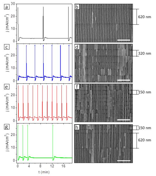
I-t transients of pulsed anodizations in which the tMA has been varied: (a) tMA = 530 s, (c) tMA = 180 s, (e) tMA = 100 s. (g) shows the I-t plot of a pulsed anodization in which two different tMA have been applied: tMA, 1 = 100 s, and tMA, 2 = 530 s. SEM images of the AAOs obtained thereof are shown in (b), (d), (f), and (h), respectively. The distance between transversal nanochannels are: (b) 620 nm (tMA = 530 s), (d) 320 nm (tMA = 180 s), and (f) 150 nm (tMA = 100 s). When two distinct tMA are applied, an AAO with two different separations between transversal nanochannels can be prepared, as evidenced in (h). Scale bars correspond to 500 nm.
Fabrication of 3D nanostructures composed of functional materials
Lastly, we show here our results on the fabrication of 3D nanostructures using the 3D-AAO templates. 3D-nanowire-like periodic nanostructures made of Bi2Te3 and other polymers like polystyrene (PS) have been fabricated 27, 28, 29 in order to demonstrate the suitability of our templates both to grow three-dimensional organic and inorganic materials.
Figure 6a and 6b show the cross-sectional SEM images of a 3D-AAO containing a Bi2Te3 3D periodic nanowire-like network prepared by pulsed electrodeposition.34 Figure 6c shows an optical micrograph of the material, in which the green colored area is where the Bi2Te3 was grown and the yellow areas correspond to the gold substrate used as electrode. The scale bar corresponds to 1 cm in this image. Note the change in color due to the Bi2Te3 nanowire network as compared with empty 3D-AAO (Figure 2c) or the black color when nanowires are prepared in a conventional AAO template.
Figure 6. 3D-Bi2Te3 and 3D-PS nanostructured materials.
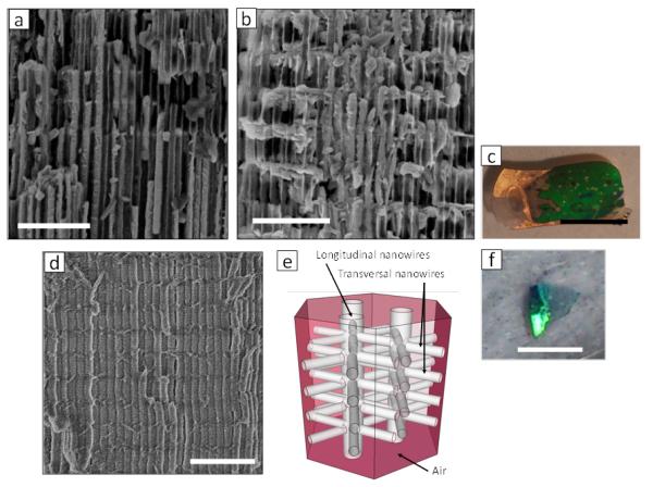
(a) and (b) Cross-sectional SEM micrographs of a three-dimensional periodic nanostructure (3D-periodic nanostructures) of the semiconductor Bi2Te3 electrodeposited inside a 3D-AAO template (VMA=25 V, tMA=180 s, VHA,N=32 V, tHA= 2 s). Scale bars correspond to 500 nm. (c) Optical photograph of the template after Bi2Te3 filling, the black bar is 1 cm. (d) Cross-sectional SEM micrograph of a three-dimensional periodic nanostructure (3D-periodic nanostructures) of polystyrene (PS) after removal of the 3D-AAO (VMA=25 V, tMA=180 s, VHA,N=32 V, tHA= 2 s). Scale bars correspond to 500 nm. (e) Sketch of the observed interconnected nanowire array. And (f) Optical photograph of the freestanding polystyrene 3D nanowire network after alumina removal, the black bar is 1 cm.
Moreover, a 3D nanowire-like network is also fabricated in polystyrene. Figure 6d shows the cross section of such material after the removal of the 3D-AAO template in NaOH. Thus a free-standing network of nanowires is shown as is represented in Figure 6e. Note that the greenish color of Figure 6f is due exclusively to the nano-architecture, since bulk PS is transparent. The scale bar corresponds to 1 cm in this image. This example constitutes a clear demonstration of the efficacy of our template to nanostructure low surface energy materials.
Other examples of functional polymers infiltrated in 3D-AAO templates are shown on Figure 7. Figure 7a shows a set of photographs (from different viewing angles) of the conjugated polymer poly[[9-(1-octylnonyl)-9H-carbazole-2,7-diyl]-2,5-thiophenediyl-2,1,3-benzothiadiazole-4,7-diyl-2,5-thiophenediyl] (PCDTBT) inside 3D AAO (VMA=25 V, tMA=180 s, VHA,N=32 V, tHA= 2 s). The different colors observed as a function of the eye angle are the direct consequence of the diffraction grating generated by the PCDTBT-filled transversal nanochannels and the alumina layers (supplementary Movie 1, recorded with a cellphone). More examples of light emitting materials prepared by infiltrating conjugated polymers such as copolymer based on fluorene, thiophene and benzothiazole (PFO-DTBT), poly(3-ethyl acetate thiophene-2,5-diyl) (P3EAT), poly(phenylene vinylene) (PPV)) into 3D-AAOs are presented in Figure 7b. The photographs are acquired under black light. Finally, composite materials showing complex response -electrical and optical for instance- can be prepared by infiltrating an electroactive polymer -such as the ferroelectric poly(vinylidene flouride-co-trifluoroethylene) (PVDF-TrFE)- into the 3D-AAO (Figure 7c).
Figure 7. 3D-AAO – functional polymer composite materials.
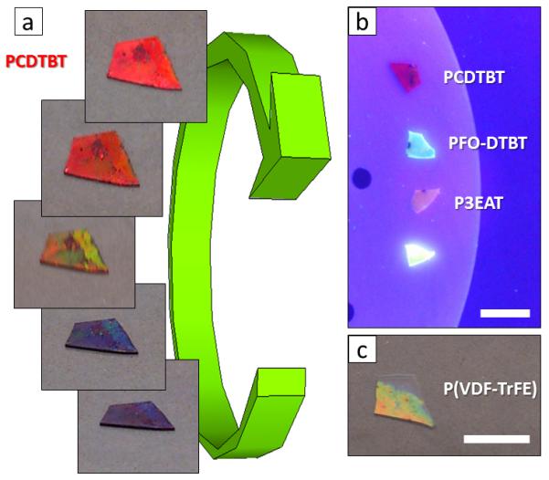
(a) Optical images of a 3D AAO (VMA=25 V, tMA=180 s, VHA,N=32 V, tHA= 2 s) infiltrated with PCDTBT polymer observed from different rotation angles. A video recorded with a cellphone can be found in the Supplementary Movie 1. (b) Photographs of 3D-AAO templates infiltrated with different conjugated polymers acquired under dark light. From top: PCDTBT, a copolymer based on fluorene, thiophene and benzothiazole (PFO-DTBT), poly(3-ethyl acetate thiophene-2,5-diyl) (P3EAT), and poly(phenylene vinylene) (PPV). Scale bars correspond to 1 cm. (c) Photographs of a 3D-AAO template infiltrated with the ferroelectric polymer poly(vinylidene flouride-co-trifluoroethylene) (PVDF-TrFE). Scale bars correspond to 1 cm.
Optical properties of the 3D AAO and nanowire networks
The optical properties of the 3D AAO were investigated by UVvis spectroscopy. The reflectance spectrum obtained from a 3D-AAO constructed on a glass substrate is seen in Figure 8a. The distance between transversal nanochannels was 320 nm in this sample, whereas the number of MA/HA bilayers amounted to 60. Both the reflectance and transmittance spectra (in the Supplementary Figure 7) show a well-defined optical band gap centered at ≈650 nm, as corresponding to a periodicity of ≈320 nm (see the SEM micrograph in Figure 8b). Note that an analogous porous alumina having only longitudinal nanopores (named as “common AAO”) shows an almost flat reflectance (Figure 8c) and transmittance spectra (Supplementary Figure 7). Thus, the 3D-AAOs enable one to easily fabricate highly tunable distributed Bragg reflectors (DBRs) in which both the distance between the alternating layers and the refraction index can be fully modulated. The periodicity can be easily modulated trough the length of the mild anodization periods, while the refraction index can be tuned by infiltrating the 3D template with materials having the desired refractive index, such as polymers from solutions (for example, following the approach showed in the Figure 7). Note that this 3D-AAO might also serve to fabricate better distributed Bragg reflector (DBR) and anisotropic 3D photonic structures as its photonic properties will be different in the in-plane and cross-plane directions. But, more interesting are the optical properties of the 3D nanowire networks fabricated from the 3D-AAO. We demonstrate here that employing 3D-AAOs, one can easy produce cheap 1D photonic crystals, even made of a “simple” and popular commodity plastic as polystyrene (PS). Figure 8d shows the reflectance spectrum of the PS 3D nanowire network shown in Figure 8e. Again, an intense reflection band at ≈525 nm can be observed as a consequence of the alternation of layers with different refractive index. This reflection band at ≈525 nm is responsible of the strong green color of this PS piece. Note that bulk PS is absolutely colorless. The PS nanowire network was prepared form a 3D AAO having a periodicity of ≈320 nm; however, the band gap in the PS 3D nanostructure is blue-shifted (≈525 nm) probably as a consequence of a shrinkage or relaxation process of the nanostructure after the 3DAAO template removal.
Figure 8. Optical properties of 3D nanostructuctures.
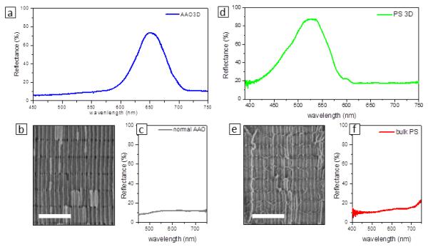
(a) Reflectance spectrum obtained from the 3D AAO shown in (b). (c) Reflectance spectrum of an AAO without transversal nanocannels (named as “common AAO“). (d) Reflectance spectra of the PS nanowire network shown in (e). (f) Reflectance spectrum of a non-porous PS (named as “bulk PS“). Scale bars in SEM micrographs correspond to 500 nm.
Discussion
A nanoporous anodic aluminum oxide (AAO) template has been prepared having a well-defined and homogeneous periodic 3D nanotubular network. The used fabrication approach includes a new type of pulsed anodization process, in which Mild Anodization (MA) and Hard Anodization (HA) pulses are alternated. The voltage here is maintained constant during MA steps, while during HA pulses the current is limited to a fixed value. This current limitation is the responsable of the high uniformity of the 3D nanostructure over the macroscopic piece, which yields a real 3D ordered nanostructure. The preferential chemical etching of the aluminum oxide grown under HA regime led then to the formation of transversal nanochannels, which interconnect adjadcent longitudinal nanopores. The 3D-AAO thus formed consists of a hexagonal array of longitudinal nanopores, perpendicularly interconnected through transversal nanochannels. 3D nanoporous networks with thickness above 20 μm in the template cross-plane direction are prepared, but size limitation on this matter is not expected. Likewise, the lateral extension of the network prepared is in the order of cm2 and limitations are neither expected. The number and the distance between planes containing the transversal nanopores can be precisely tailored selecting the amount and the length of the MA steps, which allow the modulation of the pore density of the templates. The distance between longitudinal nanopores is 65 nm. The diameter of longitudinal nanopores is 40 nm, while the section of the transversal nanochannels, which is ellipsoid, presents a short diameter of 20 nm and a large diameter of approximately 35 nm.
3D-AAOs serve as templates for the fabrication of 3D periodic nanowire-like networks in a wide variety of materials with applications in thermoelectricity, catalysis, filtration, energy storage, photonics, and the like. Thereby, we show the first attempts to the fabrication of 3D periodic nanowire-like nanostructures made of polystyrene and Bi2Te3, as well as 3D-composite nanostructures comprised of functional polymers. The development of such a versatile, rapid, low cost, industrially scalable processing route that allows efficient and controlled deposition of materials into structures with complex behavior and complex geometries –Al pieces having any shape can be anodized- can be expected to impinge on a variety of fields, from information lighting, to sensing, to coating, to biomedicine. Thereby, we have demonstrated the 1D photonic crystal behaviour of both the 3D AAO and a 3D periodic nanowire-like networks made of a commodity plastic as polystyrene. Hence, through these new materials and procedures, we might be presenting here the foundations for future high-throughput, cheap, photonic materials and devices made of simple commodity plastics.
Methods
Preparation of the 3D-AAO templates
AAO templates having periodic 3D nanotubular network templates have been prepared by a two-step anodization of aluminum,35 being the second anodization process a pulsed anodization. To begin with, ultrapure (99.999%) aluminum foils (Advent Research Materials, England), were cleaned and degreased by sonication in acetone, water, isopropanol, and ethanol. Foils were then electropolished in a solution of perchloric acid/ethanol (1/3) under a constant voltage of 20 V for 4 min. After that, the first anodization was achieved for 24 h. A 0.3 M sulphuric acid (Panreac AC Química, Spain) solution was used under a voltage of 25 V and at 0 °C. Then, the first anodic layer was removed by chemical etching in a mixture of phosphoric acid (7 wt. %) and chromic oxide (1.8 wt. %). A pulsed anodization process was then carried out in the conditions specified along the text. Afterwards, the underlying Aluminum substrate was etched with an acidic solution of CuCl2 at 1 °C and the barrier layer was dissolved using a 10 wt. % aqueous H3PO4 solution at 30 °C. Finally, the samples were submerged into a 5 wt. % aqueous H3PO4 solution at 30 °C in order to create the transversal nanochannels.
Characterization
The morphology study of 3D-AAO was performed by Scanning Electron Microscopy (SEM, Hitachi SU8000) operating at an accelerating voltage of 2 kV to avoid the deposit of any conducting layer and charging. The microscope had been properly calibrated by the operators from Hitachi, Ltd. Also, the accuracy of the measurement was checked in previous works. Ellipsometry measurements were carried out (M2000FI J.A. WoollamCo.) between 350 and 1640 nm wavelength and with incidence angles of 50°, 60°, and 70°. The samples specifically prepared for ellipsometry measurements are described in the Supplementary Note 3. The Complete Ease simulation software was used to fit the measured values of the real and imaginary parts of the dielectric tensor to Psi and Delta of the different samples. Spectroscopic reflection and transmission measurements were carried out on a Olympus BX51 microscope with 20x magnification and detected with an Ocean Optics QE 65000 spectrometer.
3D-nanowire-like periodic nanostructures made of polystyrene and Bi2Te3
For the fabrication of the 3D-nanowire-like periodic nanostructures made of polystyrene (PS), the 3D-AAO was submerged into styrene (Aldrich Ltd.) for 1h in order to induce the infiltration of the monomer into the tubular cavity. Then the styrene was polymerized using AIBN (Aldrich Ltd.) as initiator under N2 atmosphere. In the case of Bi2Te3, it was electrodeposited into the 3D-AAO template for 8 hours pulsing 0.1 s at 20 mV and 0.1 s at J= 0 mA/cm2 vs. Ag/AgCl.34 A potentiostat-galvanostat (Eco Chemie, Model AUT302.0) and a three electrode cell were used for electrodeposition.
3D-Composite materials composed of 3D-AAO and functional polymers
To fabricate the composite materials, 3D-AAOs were infiltrated with 4g/L chloroform solutions of poly[[9-(1-octylnonyl)-9H-carbazole-2,7-diyl]-2,5-thiophenediyl-2,1,3-benzothiadiazole-4,7-diyl-2,5-thiophenediyl] (PCDTBT), fluorene, thiophene and benzothiazole copolymer (PFO-DTBT), poly(3-ethyl acetate thiophene-2,5-diyl) (P3EAT), poly(phenylene vinylene) (PPV), and 5 wt. % solution of poly(vinylidene flouride-co-trifluoroethylene) (PVDF-TrFE) in dimethylformamide.
Supplementary Material
Acknowledgements
The authors would like to acknowledge financial support from ERC 2008 Starting Grant “Nano-TEC” number 240497. We thank Dr. Pablo Diaz-Chao and David Solis for their contribution in developing and improving the Labview code for controlling the growth of these templates, and Dr. Jon Maiz for his help with a sample preparation.
Footnotes
Supplementary Information accompanies this paper at https://www.nature.com/naturecommunications.
Competing financial interests: The authors declare that a patent has being filled and that the work was developed under an ERC grant.
References
- 1.Hu J, Odom TW, Lieber CM. Chemistry and Physics in One Dimension: Synthesis and Properties of Nanowires and Nanotubes. Acc. Che. Res. 1999;32:435–445. [Google Scholar]
- 2.Choi SY, Mamak M, von Freymann G, Chopra N, Ozin GA. Mesoporous Bragg Stack Color Tunable Sensors. Nano Lett. 2006;6:2456–2461. doi: 10.1021/nl061580m. [DOI] [PubMed] [Google Scholar]
- 3.Bonifacio LD, Puzzo DP, Breslav S, Willey BM, McGeer A, Ozin GA. Towards the Photonic Nose: A Novel Platform for Molecule and Bacteria Identification. Adv. Mater. 2010;22:1351–1354. doi: 10.1002/adma.200902763. [DOI] [PubMed] [Google Scholar]
- 4.Scherer MRJ, Li L, Cunha PMS, Scherman OA, Steiner U. Enhanced Electrochromism in Gyroid-Structured Vanadium Pentoxide. Adv. Mater. 2012;24:1217–1221. doi: 10.1002/adma.201104272. [DOI] [PubMed] [Google Scholar]
- 5.Scherer MRJ, Steiner U. Efficient Electrochromic Devices Made from 3D Nanotubular Gyroid Networks. Nano Lett. 2012;13:3005–3010. doi: 10.1021/nl303833h. [DOI] [PubMed] [Google Scholar]
- 6.Crossland EJW, et al. Block Copolymer Morphologies in Dye-Sensitized Solar Cells: Probing the Photovoltaic Structure–Function Relation. Nano Lett. 2008;9:2813–2819. doi: 10.1021/nl800942c. [DOI] [PubMed] [Google Scholar]
- 7.Crossland EJW, et al. A Bicontinuous Double Gyroid Hybrid Solar Cell. Nano Lett. 2008;9:2807–2812. doi: 10.1021/nl803174p. [DOI] [PubMed] [Google Scholar]
- 8.Liu R, Duay J, Lee SB. Heterogeneous nanostructured electrode materials for electrochemical energy storage. Chem.Commun. 2011;47:1384–1404. doi: 10.1039/c0cc03158e. [DOI] [PubMed] [Google Scholar]
- 9.Duay J, Gillette E, Hu J, Lee SB. Controlled electrochemical deposition and transformation of hetero-nanoarchitectured electrodes for energy storage. Phys. Chem. Chem. Phys. 2013;15:7976–7993. doi: 10.1039/c3cp50724f. [DOI] [PubMed] [Google Scholar]
- 10.Wei D, Scherer MRJ, Bower C, Andrew P, Ryhänen T, Steiner U. A Nanostructured Electrochromic Supercapacitor. Nano Letters. 2012;12:1857–1862. doi: 10.1021/nl2042112. [DOI] [PubMed] [Google Scholar]
- 11.Jang D, Meza LR, Greer F, Greer JR. Fabrication and deformation of three-dimensional hollow ceramic nanostructures. Nat. Mater. 2013;12:893–898. doi: 10.1038/nmat3738. [DOI] [PubMed] [Google Scholar]
- 12.Vignolini S, et al. A 3D Optical Metamaterial Made by Self-Assembly. Adv. Mater. 2012;24:OP23–OP27. doi: 10.1002/adma.201103610. [DOI] [PubMed] [Google Scholar]
- 13.Galisteo-López JF, Ibisate M, Sapienza R, Froufe-Pérez LS, Blanco Á , López C. Self-Assembled Photonic Structures. Adv. Mater. 2011;23:30–69. doi: 10.1002/adma.201000356. [DOI] [PubMed] [Google Scholar]
- 14.Rauber M, et al. Highly-Ordered Supportless Three-Dimensional Nanowire Networks with Tunable Complexity and Interwire Connectivity for Device Integration. Nano Lett. 2011;11:2304–2310. doi: 10.1021/nl2005516. [DOI] [PubMed] [Google Scholar]
- 15.Vukovic I, Brinke Gt, Loos K. Block copolymer template-directed synthesis of well-ordered metallic nanostructures. Polymer. 2013;54:2591–2605. [Google Scholar]
- 16.Hsueh H-Y, Ho R-M. Bicontinuous Ceramics with High Surface Area from Block Copolymer Templates. Langmuir. 2012;28:8518–8529. doi: 10.1021/la3009706. [DOI] [PubMed] [Google Scholar]
- 17.Lee W, Kim J-C, Gösele U. Spontaneous Current Oscillations during Hard Anodization of Aluminum under Potentiostatic Conditions. Adv. Funct. Mater. 2010;20:21–27. [Google Scholar]
- 18.Wang W, Tian M, Abdulagatov A, George SM, Lee Y-C, Yang R. Three-Dimensional Ni/TiO2 Nanowire Network for High Areal Capacity Lithium Ion Microbattery Applications. Nano Lett. 2011;12:655–660. doi: 10.1021/nl203434g. [DOI] [PubMed] [Google Scholar]
- 19.Losic D. Preparation of Porous Anodic Alumina with Periodically Perforated Pores. Langmuir. 2009;25:5426–5431. doi: 10.1021/la804281v. [DOI] [PubMed] [Google Scholar]
- 20.Lee W, Schwirn K, Steinhart M, Pippel E, Scholz R, Gosele U. Structural engineering of nanoporous anodic aluminium oxide by pulse anodization of aluminium. Nat. Nanotech. 2008;3:234–239. doi: 10.1038/nnano.2008.54. [DOI] [PubMed] [Google Scholar]
- 21.Lee W, Kim J-C. Highly ordered porous alumina with tailor-made pore structures fabricated by pulse anodization. Nanotechnology. 2010;21:485304. doi: 10.1088/0957-4484/21/48/485304. [DOI] [PubMed] [Google Scholar]
- 22.Lee W, Scholz R, Gosele U. A Continuous Process for Structurally Well-Defined Al2O3 Nanotubes Based on Pulse Anodization of Aluminum. Nano Lett. 2008;8:2155–2160. doi: 10.1021/nl080280x. [DOI] [PubMed] [Google Scholar]
- 23.Sulka GD, Brzózka A, Liu L. Fabrication of diameter-modulated and ultrathin porous nanowires in anodic aluminum oxide templates. Electrochim. Acta. 2011;56:4972–4979. [Google Scholar]
- 24.Martín-González M, Caballero-Calero O, Díaz-Chao P. Nanoengineering thermoelectrics for 21st century: Energy harvesting and other trends in the field. Renewable Sustainable Energy Rev. 2013;24:288–305. [Google Scholar]
- 25.Yu J-S, Kang S, Yoon SB, Chai G. Fabrication of Ordered Uniform Porous Carbon Networks and Their Application to a Catalyst Supporter. J. Am. Chem. Soc. 2002;124:9382–9383. doi: 10.1021/ja0203972. [DOI] [PubMed] [Google Scholar]
- 26.Yang SY, Ryu I, Kim HY, Kim JK, Jang SK, Russell TP. Nanoporous Membranes with Ultrahigh Selectivity and Flux for the Filtration of Viruses. Adv. Mater. 2006;18:709–712. [Google Scholar]
- 27.Martín-González M, Prieto AL, Gronsky R, Sands T, Stacy AM. Insights into the electrodeposition mechanisms of Bi2Te3 J. Electrochem. Soc. 2002;149:C546–C554. [Google Scholar]
- 28.Caballero-Calero O, Díaz-Chao P, Abad B, Manzano CV, Ynsa MD, Romero JJ, Muñoz Rojo M, Martín-González MS. Improvement of Bismuth Telluride electrodeposited films by the addition of Sodium Lignosulfonate. Electrochim. Acta. 2014;123:117–126. [Google Scholar]
- 29.Martín-González M, Snyder GJ, Prieto AL, Gronsky R, Sands T, Stacy AM. Direct Electrodeposition of Highly Dense 50 nm Bi2Te3-ySey Nanowire Arrays. Nano Lett. 2003;3:973–977. [Google Scholar]
- 30.Schwirn K, Lee W, Hillebrand R, Steinhart M, Nielsch K, Gösele U. Self-Ordered Anodic Aluminum Oxide Formed by H2SO4 Hard Anodization. ACS Nano. 2008;2:302–310. doi: 10.1021/nn7001322. [DOI] [PubMed] [Google Scholar]
- 31.Martín J, Manzano CV, Caballero-Calero O, Martín-González M. High-Aspect-Ratio and Highly Ordered 15-nm Porous Alumina Templates. ACS Appl. Mater. Interfaces. 2013;5:72–79. doi: 10.1021/am3020718. [DOI] [PubMed] [Google Scholar]
- 32.Manzano CV, Martín J, Martín-González M. Ultra-narrow 12 nm pore diameter self-ordered anodic alumina templates. Micropor. Mesopor. Mat. 2014;184:177–183. [Google Scholar]
- 33.Losic D, Lillo M. Porous Alumina with Shaped Pore Geometries and Complex Pore Architectures Fabricated by Cyclic Anodization. Small. 2009;5:1392–1397. doi: 10.1002/smll.200801645. [DOI] [PubMed] [Google Scholar]
- 34.Manzano CV, Rojas AA, Decepida M, Abad B, Feliz Y, Caballero-Calero O, Borca-Tasciuc D-A, Martin-Gonzalez M. Thermoelectric properties of Bi2Te3 films by constant and pulsed electrodeposition. J. Solid State Electrochem. 2013;17:2071–2078. [Google Scholar]
- 35.Masuda H, Satoh M. Fabrication of Gold Nanodot Array Using Anodic Porous Alumina as an Evaporation Mask. Jpn. J. Appl. Phys. 1996;35:L126. [Google Scholar]
Associated Data
This section collects any data citations, data availability statements, or supplementary materials included in this article.


