Abstract
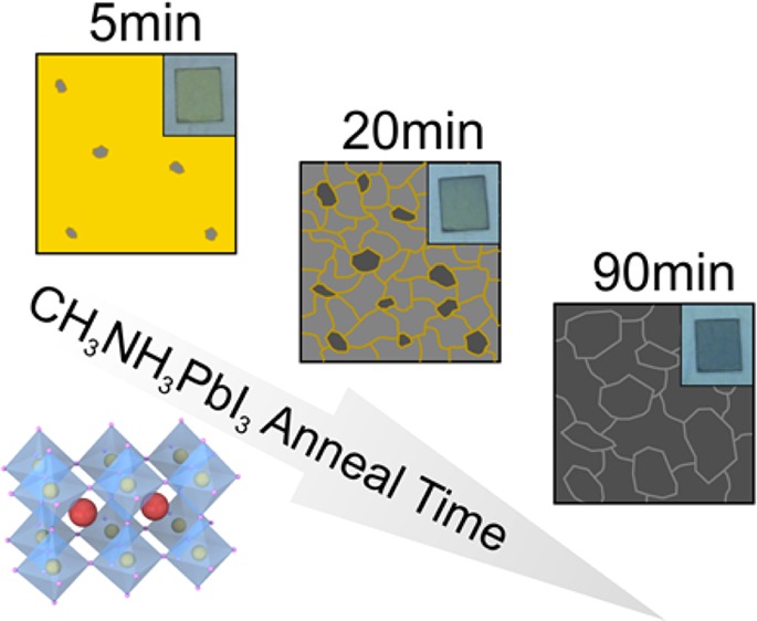
In this work we demonstrate that the different processes occurring during hybrid organic–inorganic lead iodide perovskite film formation can be identified and analyzed by a combined in situ analysis of their photophysical and structural properties. Our observations indicate that this approach permits unambiguously identifying the crystal nucleation and growth regimes that lead to the final material having a cubic crystallographic phase, which stabilizes to the well-known tetragonal phase upon cooling to room temperature. Strong correlation between the dynamic and static photoemission results and the temperature-dependent X-ray diffraction data allows us to provide a description and to establish an approximate time scale for each one of the stages and their evolution. The combined characterization approach herein explored yields key information about the kinetics of the process, such as the link between the evolution of the defect density during film formation, revealed by a fluctuating photoluminescence quantum yield, and the gradual changes observed in the PbI2-related precursor structure.
Introduction
Ever since the first evidence that hybrid organic–inorganic lead-halide perovskites could outperform all other solution process approaches to fabricate photovoltaic devices,1−5 strong research efforts have been directed mainly in two directions: looking for the best solar-cell configuration (with recent reports pointing to performances rapidly approaching that of well established single crystal silicon cells6) and exploring more fundamental questions, essential to translating the current perovskite solar cell rush into a well-established technology. The latter includes the nature of photoexcited species, stability of the material under operating conditions, the reproducibility of efficiency measurements, the synthesis of the material, and so on.7,8 Regarding its synthesis, a number of approaches have been explored to prepare high-quality perovskite films ranging from vacuum evaporation9,10 to solution process techniques.11−13 Among the latter, spin coating is the most widespread approach representing the best compromise between material quality, feasibility of mass-production, and low-cost processing, leading to high-performance photovoltaic devices as well as light-emitting ones with outstanding efficiency.14
The morphology of the fabricated material (crystal size distribution and shape as well as their connectivity and final film texture), determining its operation in both photovoltaic and emitting materials is strongly determined by the growth process. In this respect, a number of articles12,15−24 have recently studied the steps that link the initial precursors to the final material during the solution process of organic–inorganic lead halide perovskite (CH3NH3PbX3, where X corresponds to Cl, Br, or I) films. These studies, carried out mainly from structural information concerning electron microscopy images and X-ray diffraction (XRD) experiments, have focused on different aspects of the material formation. These include the effect of annealing conditions,15,20 and its rate,16 the evolution of the crystallization process,12,18,21,24 or the nature of the intermediate precursor species that precede perovskite formation,12,17,19,21,22 all of them leading to the fabrication of samples with better crystalline quality.
In this work we present a combined optical and structural study comprising the time evolution of the photoluminescence (PL) spectra and decay rates as well as the XRD collected in situ during the annealing in air of CH3NH3PbI3 films just after spin coating the precursors of the material. While only two stages in material formation are evident from XRD data, its combination with photophysical measurements reveals four different time intervals where nucleation of crystallites and subsequent crystal growth seem to dominate. Strong fluctuations in the PL quantum yield are evident throughout the process and correlated with the evolution of PbI2-related precursor species and sample morphology. A full time line for the perovskite formation is proposed that could help to improve the material quality by modifying the process at each of the different steps. Finally, once the annealing process has come to an end, changes in the photophysical and structural properties evidence a transition from the cubic to the tetragonal crystalline phase upon cooling of the annealed material to room temperature.
Experimental Details
Sample Preparation
CH3NH3PbI3 films were prepared following a previously described approach13 based on a solvent-annealing crystallization method.
Photophysical Characterization
After the 20 s spin step ended samples were placed on top of a Peltier Cell set at 100 °C to carry out the photophysical study in an air atmosphere. A black metal plate was placed between the cell and the sample to avoid reflections of the pump beam. The sample was illuminated with a pulsed femtosecond laser source (OPerA-Solo from Coherent, delivering 150 fs long pulses with a repetition rate of 1 kHz and a λ = 532 nm) focused with an achromatic 10 cm focal length lens producing a spot size of 40 μm, which also acted as collection optics. PL spectra were collected with a fiber-coupled spectrophotometer (USB4000 from Ocean Optics). Lifetime measurements were carried out using a time-correlated single photon counting card (SPC-130 from Becker & Hickl).
XRD Measurements
Temperature-controlled XRD measurements were collected in a Philips X’pert PRO diffractometer with a high-temperature chamber (ANTON PAAR HTK 1200) attached. Acquisition of the samples was taken in the 5–20 2θ range with a 0.05 step in air atmosphere.
Results and Discussion
After annealing over a period of 90 min, the samples, comprising films having large (over 1 μm dimensions in-plane) domains with a thickness of 300 nm (see Figure S1), present a strong PL peak centered at 770 nm. Lifetime measurements were performed for an increasing pump power ranging from 10 nw to 2 μW, and the appropriate pump conditions were extracted to ensure that we are in the monomolecular recombination regime (see Figure S2). Under these conditions recombination dynamics are dominated by the filling of trap states associated with the presence of defects.25,26 Studying the photophysics in this regime is relevant to take into account the role of defects during the sample formation. Next we focused on the heating process commonly used to anneal the perovskites. As a first step XRD data were collected as a function of time while the sample was heated to 100 °C. Figure 1a,b shows data taken at two times of the heating process, 1 and 100 min after precursor deposition. This time interval allows the sample to achieve a region where material formation seems complete and no signs of degradation (such as the characteristic color change to yellow or changes in the XRD or PL data) were observed. In the angular range under consideration two peaks were studied: one around 2θ = 14° characteristic of the (110) planes of the tetragonal CH3NH3PbI3 phase or the (100) of the cubic phase (detailed crystallographic information on the different CH3NH3PbI3 phases has been provided by Baikie and coworkers27) and another just below 2θ = 12° associated with intermediate PbI2-related precursor species, which will get consumed during perovskite formation.18 Both peaks appear highlighted by arrows in the Figure. To follow the evolution of both species during annealing we have extracted the intensity maxima of each peak as a function of time.
Figure 1.
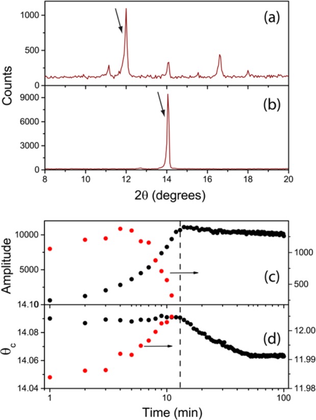
XRD data of thin-film perovskites collected at two points of the annealing process: 1 (a) and 100 min (b) after precursor deposition. Diffraction peaks associated with CH3NH3PbI3 and PbI2-related precursors are indicated with arrows. Evolution of the intensity maximum of the XRD peak (c) corresponding to CH3NH3PbI3 (black) and precursor species (red circles) and angular position (d) as a function of anneal time.
A trend similar to that presented by Unger and coworkers18 and Moore and coworkers19 is observed, where a monotonic increase in the CH3NH3PbI3 related peak is accompanied by a drop in the peak associated with the presence of the intermediate precursor species (see Figure 1c). Such trends indicate the formation of the perovskite species as the lead precursor disappears. Ref (19) presents an analysis of this evolution from which they extract the activation energy for the precursor-to-perovskite transition but does not allow discerning between the nucleation and crystal growth processes involved in the CH3NH3PbI3 formation. We have further extracted the angular position of the peaks corresponding to the two species, a small shift in the position being evident (Figure 1d). We shall come back to this point later on.
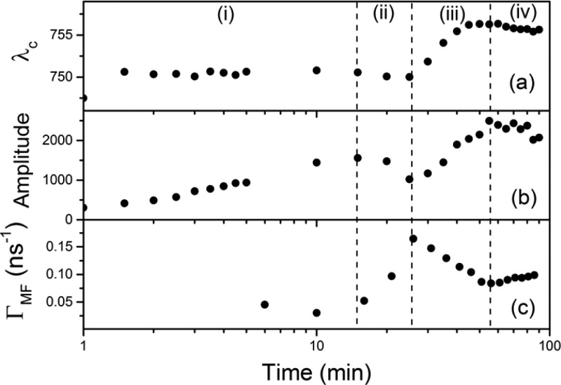
To gain further knowledge into the formation process we have studied the photophysics of the samples during annealing. As a first step, PL spectra were collected at different times of the process (T = 100 °C) while the sample was pumped with 500 nW. Furthermore, for the power and small duty cycle associated with these pump conditions no changes in intensity due to photoinduced processes28 were observed. Figure 2a,b shows the spectral position and amplitude of the PL peak as a function of anneal time. Here four different regimes can be clearly observed. For a time interval (i) similar to that taken by PbI2-related precursor species to disappear (ca. 15 min, see Figure 1c) the PL peak remains fixed in spectral position but monotonically increases its intensity. After a 10 min interval where the PL intensity slightly decreases while maintaining its spectral position, stage (ii), the PL further rises in amplitude and is accompanied by a red shift in the peak. This period (iii) lasts nearly 30 min and then a final stage is achieved (iv), which we identify with the end of the annealing process. The time needed to reach this last stage is similar to previous reports where the crystallization of the perovskite film was considered completed.12,18
Figure 2.
Time evolution during the annealing process of spectral position (a) and amplitude (b) of the PL peak and most frequent value of the decay rate distribution (c). Four regimes corresponding to four different perovskite film formation stages (see text) are separated by vertical dashed lines.
Finally, we have performed time-resolved measurements to obtain the PL decay dynamics of the material during its formation in the annealing process. Under the previously mentioned pump conditions we are in the monomolecular recombination regime (see Figure S2) where the presence of defects determines the dynamics of the PL and thus changes in the density of trap states are expected to be reflected in the PL lifetime. Measurements were carried out on different samples than those used for XRD although under identical heating conditions to compare them. The dynamics of the PL of the deposited samples were observed to strongly vary as the annealing time increased (see Figure S3). To correlate these changes with those previously described, we fitted the data to a decay rate distribution and extracted the most frequent value for each annealing time (ΓMF). Figure 2c shows the time evolution of the decay rates, where measurements were collected over a period of 5 min to have enough signal. As for XRD data, PL decay measurements were repeated on different samples and similar results were obtained.
During stage (i) the monotonic increase in PL intensity (Figure 2b) coincides with the rise of the amplitude of the XRD peak corresponding to the perovskite (Figure 1c), evidencing the formation of CH3NH3PbI3 as more crystals contribute to Bragg diffraction. Also during this interval the angular position, as seen in Figure 1d (black dots), and width (not shown) of the XRD peak do not vary. This data indicates that stage (i) corresponds to the nucleation of perovskite crystallites during the annealing process.
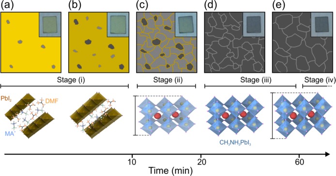
If we consider now the PL decay dynamics (Figure 2c) we see how during stage (ii) a rapid increase in the decay rate takes place. This is accompanied by a decrease in the PL intensity. These changes point to a decrease in the quantum yield (QY) of the material, likely related to the presence of nonradiative recombination paths associated with crystalline defects. This drop in the QY coincides with the vanishing of the XRD intensity of the PbI2-related precursor (Figure 1c) which seems to be acting as a “passivating” agent of the formed crystallites. If one considers the angular position of the precursor XRD peak (red dots in Figure 1d), the drop of its intensity is accompanied by a shift to larger angles closer to the value expected for pure PbI2.29 A plausible explanation for this behavior is illustrated in Figure 3, where a schematic description of the crystal growth process is provided along with the concomitant changes in the precursor and perovskite structures.
Figure 3.
Schematic representation of the CH3NH3PbI3 formation during the annealing process. (a,b) Perovskite crystallites (gray regions) form in a medium comprising a PbI2-related precursor (yellow region). (c) All crystallites form at the expense of the precursor. (d,e) Crystal growth takes place as different crystallites coalesce. Insets show photographs of the samples at different stages of the annealing process: 5, 10, 20, 40, and 90 min.
The perovskite crystallites form in the presence of a precursor whose nature could be PbI2 planes intercalated with DMF as well as MAI molecules, which separate the crystallographic planes of the inorganic material (Figure 3a,b).30 As nucleation proceeds, new perovskite crystallites form and the intercalated DMF molecules evaporate, causing the PbI2 planes to become closer together, this being at the origin of the narrower interplanar spacing revealed in Figure 1d (red dots). At a certain point, corresponding to the stage (ii), all crystallites are formed at the expense of the precursor. As it disappears, the newly formed grain boundaries (Figure 3c) introduce carrier traps that act as nonradiative decay paths that yield the sudden drop of photoemission efficiency observed (Figure 2b). This time interval corresponds to the early stages of the annealing process for which previous work has reported the existence of intermediate precursor species.12,17,19,21,22
As we enter the third regime (iii) the PL decay rate monotonically decreases until it reaches the constant value characteristic of region (iv). This is accompanied by a number of changes in some of the other magnitudes we have monitored. As the amplitude of the XRD peak associated with the crystalline CH3NH3PbI3 remains constant we assume that the total amount of perovskite does not change. At this point, crystal growth of large domains at the expense of smaller crystallites is probably taking over (Figure 3d,e). This is in agreement with the fact that the PL intensity further increases (see Figure 2b), as larger crystallites present a smaller density of surface defects that are expected to reduce the QY of the material. The hypothesis of crystal growth is further supported by a red shift of the PL peak (Figure 2a) and a decrease in the decay dynamics. This behavior has been previously observed by D’Innocenzo and coworkers31 as a signature of increasing perovskite crystal size. In that work, the origin of this behavior was attributed to the release of strain present in the crystalline lattice as a consequence of the distortion of the Pb–I–Pb bond. This is in agreement with the monotonic enlargement of the interplanar spacing revealed by the change in the position of the XRD peak associated with the CH3NH3PbI3 (see black dots in Figure 1d) during this third time interval. Indeed, a difference in the XRD peak position of similar magnitude has been observed when comparing CH3NH3PbI3 grown on a flat substrate and in a mesostructure, the latter constraining the space for crystal growth.23
According to this picture the annealing process necessary for the formation of CH3NH3PbI3 upon spin-coating consists of four different regimes. These comprise the nucleation of small crystallites (i), a transitional stage during which a large number of grain boundaries are formed as precursors vanish (ii), an actual crystal growth period where different crystals coalesce (iii), and a final stage (iv) where the material is eventually formed. Furthermore, this whole picture can be accessed only through the combined use of in situ XRD and photophysical measurements as certain aspects of the structural changes revealed by the former can be interpreted only through information contained in the latter.
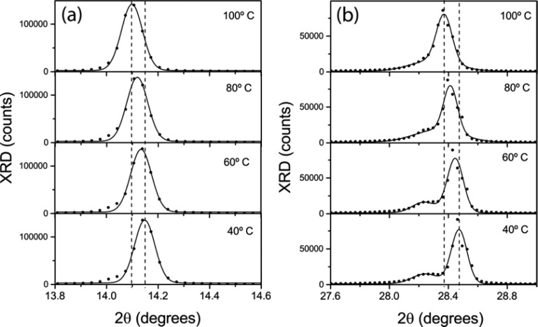
At this point we note that the photophysics of the samples at the end of the annealing process differ from those of a sample left to cool under ambient conditions for a few hours. In particular, the PL undergoes a slight red shift of ca. 15 nm (see Figure S4), similar to that recently reported as CH3NH3PbI3 films were heated and ascribed to the phase change from cubic to tetragonal expected for this material at 42–57 °C.32 As the annealing process takes place well above such temperature, the phase of the as-prepared films is then expected to be cubic, changing to tetragonal as the sample cools. As a matter of fact, XRD collected at different temperatures below the annealing one (see Figure 4) show a shift to higher angles of the diffraction peak at ∼14°. A change of similar magnitude (0.05°) is expected to take place as one considers Bragg diffraction from the (100) planes of the cubic phase and from the (110) planes of the tetragonal phase. This point is further supported by the fact that the corresponding second-order diffraction (around 28°) shifts to larger angles and splits into two, as expected from the (200) diffraction of the cubic phase and the (004) and (220) of the tetragonal phase.27 Finally, as the sample cools from the annealing temperature, the decay rate is reduced by nearly one order of magnitude. Such change is probably due to the fact that the crystallization of the sample continues once the annealing process is interrupted, albeit at a slower pace, something that has been recently observed by Yamada and coworkers.33
Figure 4.
XRD data collected as a CH3NH3PbI3 film was gradually cooled from 100 (i.e., the annealing temperature) to 40 °C. Graphs (a) and (b) correspond to angular ranges where characteristic diffraction peaks are expected for the cubic and tetragonal phases of the perovskite material. Full circles correspond to experimental data and lines are fits to a Gaussian line shape. Vertical lines highlight the angular position of the main diffraction peaks at the start and end temperatures.
Conclusions
In summary, we have studied the process of hybrid organic–inorganic perovskite formation during annealing by simultaneously carrying out real-time in situ structural and photophysical characterization. The combination of both types of experiments proves crucial to unveil different mechanisms taking place during the material formation. These include fluctuations in the PL QY associated with crystal morphology changing as precursors disappear or the transition from the as-grown cubic crystalline phase, generated during the annealing, to the well-known tetragonal phase achieved by cooling the sample to room temperature. While the transition from kinetically favorable nucleation to the thermodynamically stable crystal growth is a complicated process, from which retrieving information on the different steps is a difficult task, we believe the present results constitute a step further in understanding the process of formation of CH3NH3PbI3. Furthermore, we note that while applied for a specific synthetic route and material, the present study can be generalized as a tool to explore the processes leading to the formation of any hybrid organic–inorganic perovskite demanding a post-deposition (being solution process or vacuum) treatment. A precise knowledge of all of the intermediate stages could pave the way to a deeper control of the morphology of the perovskite material and hence of the performance of the final photovoltaic or light-emitting device.
Acknowledgments
The research leading to these results has received funding from the European Research Council under the European Union’s Seventh Framework Programme (FP7/2007-2013)/ERC Grant Agreement No. 307081 (POLIGHT) and the Spanish Ministry of Economy and Competitiveness under Grants MAT2014-54852-R and MAT2012-31659 and Comunidad de Madrid programme S2013/MIT-2740. M.A. is grateful to La Caixa Foundation for its financial support.
Supporting Information Available
The Supporting Information is available free of charge on the ACS Publications website at DOI: 10.1021/acs.jpcc.6b00398.
SEM image; PL dynamics as a function of pump intensity; fitting model for PL decays; PL decays at different stages of the annealing process; and PL spectra at the end of the annealing process and after cooling to room temperature. (PDF)
The authors declare no competing financial interest.
Supplementary Material
References
- Kojima A.; Teshima K.; Shirai Y.; Miyasaka T. Organometal Halide Perovskites as Visible-Light Sensitizers for Photovoltaic Cells. J. Am. Chem. Soc. 2009, 131, 6050–6051. 10.1021/ja809598r. [DOI] [PubMed] [Google Scholar]
- Im J. H.; Lee C. R.; Lee J. W.; Park S. W.; Park N. G. 6.5% efficient perovskite quantum-dot-sensitized solar cell. Nanoscale 2011, 3, 4088–4093. 10.1039/c1nr10867k. [DOI] [PubMed] [Google Scholar]
- Chung I.; Lee B.; He J.; Chang R. P. H.; Kanatzidis M. G. All-solid-state dye-sensitized solar cells with high efficiency. Nature 2012, 485, 486–489. 10.1038/nature11067. [DOI] [PubMed] [Google Scholar]
- Kim H. S.; Lee C. R.; Im J. H.; Lee K. B.; Moehl T.; Marchioro A.; Moon S. J.; Humphry-Baker R.; Yum J. H.; Moser J. E.; Grätzel M.; Park N. G. Lead Iodide Perovskite Sensitized All-Solid-State Submicron Thin Film Mesoscopic Solar Cell with Efficiency Exceeding 9%. Sci. Rep. 2012, 2, 591. 10.1038/srep00591. [DOI] [PMC free article] [PubMed] [Google Scholar]
- Lee M. M.; Teuscher J.; Miyasaka T.; Murakami T. N.; Snaith H. J. Efficient Hybrid Solar Cells Based on Meso-Superstructured Organometal Halide Perovskites. Science 2012, 338, 643–647. 10.1126/science.1228604. [DOI] [PubMed] [Google Scholar]
- See NREL’s Efficiency Chart (http://www.nrel.gov/ncpv/images/efficiency_chart.jpg) for the latest certified efficiency update.
- Christians J. A.; Manser J. S.; Kamat P. V. The Multifaceted Excited State of CH3NH3PbI3. Charge Separation, Recombination, and Trapping. J. Phys. Chem. Lett. 2015, 6, 2086–2095. 10.1021/acs.jpclett.5b00594. [DOI] [PubMed] [Google Scholar]
- Egger D. A.; Edri E.; Cahen D.; Hodes G. Perovskite Solar Cells: Do We Know What We Do Not Know?. J. Phys. Chem. Lett. 2015, 6, 279–282. 10.1021/jz502726b. [DOI] [PubMed] [Google Scholar]
- Liu M.; Johnston M. B.; Snaith H. J. Efficient Planar Heterojunction Perovskite Solar Cells by Vapour Deposition. Nature 2013, 501, 395–398. 10.1038/nature12509. [DOI] [PubMed] [Google Scholar]
- Chen C.-W.; Kang H.-W.; Hsiao S.-Y.; Yang P.-F.; Chiang K.-M.; Lin H.-W. Efficient and Uniform Planar-Type Perovskite Solar Cells by Simple Sequential Vacuum Deposition. Adv. Mater. 2014, 26, 6647–6652. 10.1002/adma.201402461. [DOI] [PubMed] [Google Scholar]
- Burschka J.; Pellet N.; Moon S.-J.; Humphry-Baker R.; Gao P.; Nazeeruddin M. K.; Grätzel M. Sequential Deposition as a Route to High-Performance Perovskite-Sensitized Solar Cells. Nature 2013, 499, 316–319. 10.1038/nature12340. [DOI] [PubMed] [Google Scholar]
- Jeon N. J.; Noh J. H.; Kim Y. C.; Yang W. S.; Ryu S.; Seok S. I. Solvent Engineering for High-Performance Inorganic–Organic Hybrid Perovskite Solar Cells. Nat. Mater. 2014, 13, 897–903. 10.1038/nmat4014. [DOI] [PubMed] [Google Scholar]
- Xiao M.; Huang F.; Huang W.; Dkhissi Y.; Zhu Y.; Etheridge J.; Gray-Weale A.; Bach U.; Cheng Y.-B.; Spiccia L. A Fast Deposition-Crystallization Procedure for Highly Efficient Lead Iodide Perovskite Thin-Film Solar Cells. Angew. Chem., Int. Ed. 2014, 53, 9898–9903. 10.1002/anie.201405334. [DOI] [PubMed] [Google Scholar]
- Cho H.; Jeong S.-H.; park M.-H.; Kim Y.-H.; Wolf C.; Lee C.-L.; Heo J. H.; Sadhanala A.; Myoung N.; Yoo S.; Im S. H.; Friend R. H.; Lee T.-W. Overcoming the Electroluminescence Efficiency Limitations of Perovskite Light-Emitting Diodes. Science 2015, 350, 1222–1225. 10.1126/science.aad1818. [DOI] [PubMed] [Google Scholar]
- Dualeh A.; Tétreault N.; Moehl T.; Gao P.; Nazeeruddin M. K.; Grätzel M. Effect of Annealing Temperature on Film Morphology of Organic–Inorganic Hybrid Pervoskite Solid-State Solar Cells. Adv. Funct. Mater. 2014, 24, 3250–3258. 10.1002/adfm.201304022. [DOI] [Google Scholar]
- Saliba M.; Tan K. W.; Sai H.; Moore D. T.; Scott T.; Zhang W.; Estroff L. A.; Wiesner U.; Snaith H. J. Influence of Thermal Processing Protocol upon the Crystallization and Photovoltaic Performance of Organic–Inorganic Lead Trihalide Perovskites. J. Phys. Chem. C 2014, 118, 17171–17177. 10.1021/jp500717w. [DOI] [Google Scholar]
- Tan K. W.; Moore D. T.; Saliba M.; Sai H.; Estroff L. A.; Hanrath T.; Snaith H. J.; Wiesner U. Thermally Induced Structural Evolution and Performance of Mesoporous Block Copolymer-Directed Alumina Perovskite Solar Cells. ACS Nano 2014, 8, 4730–4739. 10.1021/nn500526t. [DOI] [PMC free article] [PubMed] [Google Scholar]
- Unger L. E.; Bowring A. R.; Tassone C. J.; Pool V. L.; Gold-Parker A.; Cheacharoen R.; Stone K. H.; Hoke E. T.; Toney M. F.; McGehee M. D. Chloride in Lead Chloride-Derived Organo-Metal Halides for Perovskite-Absorber Solar Cells. Chem. Mater. 2014, 26, 7158–7165. 10.1021/cm503828b. [DOI] [Google Scholar]
- Moore D. T.; M; Sai H.; Tan K. W.; Smilgies D.-M.; Zhang W.; Snaith H. J.; Wiesner U.; Estroff L. A. Crystallization Kinetics of Organic–Inorganic Trihalide Perovskites and the Role of the Lead Anion in Crystal Growth. J. Am. Chem. Soc. 2015, 137, 2350–2358. 10.1021/ja512117e. [DOI] [PubMed] [Google Scholar]
- Xiao Z.; Dong Q.; Bi C.; Shao Y.; Yuan Y.; Huang J. Solvent Annealing of Perovskite-Induced Crystal Growth for Photovoltaic-Device Efficiency Enhancement. Adv. Mater. 2014, 26, 6503–6509. 10.1002/adma.201401685. [DOI] [PubMed] [Google Scholar]
- Zhang W.; Saliba M.; Moore D. T.; Pathak S. K.; Hörantner M. T.; Stergiopoulos T.; Stranks S. D.; Eperon G. E.; Alexander-Webber J. A.; Abate A.; Sadhanala A.; Yao S.; Chen Y.; Friend R. H.; Estroff L. A.; Wiesner U.; Snaith H. J. Ultrasmooth organic–inorganic perovskite thin-film formation and crystallization for efficient planar heterojunction solar cells. Nat. Commun. 2015, 6, 6142. 10.1038/ncomms7142. [DOI] [PubMed] [Google Scholar]
- Manser J. S.; Reid B.; Kamat P. V. Evolution of Organic-Inorganic Lead Halide Perovskite from Solid-State Iodoplumbate Complexes. J. Phys. Chem. C 2015, 119, 17065–17063. 10.1021/acs.jpcc.5b05898. [DOI] [Google Scholar]
- Grancini G.; Marras S.; Prato M.; Giannini C.; Quarti C.; De Angelis F.; De Bastiani M. D.; Eperon G. E.; Snaith H. J.; Manna L.; Petrozza A. J. The Impact of the Crystallization Processes on the Structural and Optical Properties of Hybrid Perovskite Films for Photovoltaics. J. Phys. Chem. Lett. 2014, 5, 3836–3842. 10.1021/jz501877h. [DOI] [PubMed] [Google Scholar]
- Moore D. T.; Tan K. W.; Sai H.; Barteau K. P.; Wiesner U.; Estroff L. A. Direct Crystallization Route to Methylammonium Lead Iodide Perovskite from an Ionic Liquid. Chem. Mater. 2015, 27, 3197–3199. 10.1021/cm5047484. [DOI] [Google Scholar]
- Stranks S. D.; Burlakov V. M.; Leijtens T.; Ball J. M.; Goriely A.; Snaith H. J. Recombination Kinetics in Organic–Inorganic Perovskites: Excitons, Free Charge, and Subgap States. Phys. Rev. Appl. 2014, 2, 034007. 10.1103/PhysRevApplied.2.034007. [DOI] [Google Scholar]
- Yamada Y.; Nakamura T.; Endo M.; Wakamiya A.; Kanemitsu Y. Photocarrier Recombination Dynamics in Perovskite CH3NH3PbI3 for Solar Cell Applications. J. Am. Chem. Soc. 2014, 136, 11610–11613. 10.1021/ja506624n. [DOI] [PubMed] [Google Scholar]
- Baikie T.; Fang Y.; Kadro J. M.; Schreyer M.; Wei F.; Mhaisalkar S. G.; Graetzel M.; White T. J. Synthesis and Crystal Chemistry of the Hybrid Perovskite (CH3NH3)PbI3 for Solid-State Sensitised Solar Cell Applications. J. Mater. Chem. A 2013, 1, 5628–5641. 10.1039/c3ta10518k. [DOI] [Google Scholar]
- Galisteo-López J. F.; Anaya M.; Calvo M. E.; Míguez H. Environmental effects on the photophysics of organic-inorganic halide perovskites. J. Phys. Chem. Lett. 2015, 6, 2200–2205. 10.1021/acs.jpclett.5b00785. [DOI] [PMC free article] [PubMed] [Google Scholar]
- Zheng Z.; Liu A.; Wang S.; Wang Y.; Li Z.; Lau W. M.; Zhang L. In Situ Growth of Epitaxial Lead Iodide Films Composed of Hexagonal Single Crystals. J. Mater. Chem. 2005, 15, 4555–4559. 10.1039/b510077a. [DOI] [Google Scholar]
- Shen D.; Yu X.; Cai X.; Peng M.; Ma Y.; Su X.; Xiao L.; Zou D. Understanding the Solvent-Assisted Crystallization Mechanism Inherent in Efficient Organic-Inorganic Halide Perovskite Solar Cells. J. Mater. Chem. A 2014, 2, 20454–20461. 10.1039/C4TA05635C. [DOI] [Google Scholar]
- D’Innocenzo V.; Kandada A. R. S.; De Bastiani M.; Gandini M.; Petrozza A. Tuning the Light Emission Properties by Band Gap Engineering in Hybrid Lead Halide Perovskite. J. Am. Chem. Soc. 2014, 136, 17730–17733. 10.1021/ja511198f. [DOI] [PubMed] [Google Scholar]
- Milot R. L.; Eperon G. E.; Snaith H. J.; Johnston M. B.; Herz L. M. Temperature-Dependent Charge-Carrier Dynamics in CH3NH3PbI3 Perovskite Thin Films. Adv. Funct. Mater. 2015, 25, 6218–6227. 10.1002/adfm.201502340. [DOI] [Google Scholar]
- Yamada Y.; Nakamura T.; Endo M.; Wakamiya A.; Kanemitsu Y. Spontaneous Defect Annihilation in CH3NH3PbI3 Thin Films at Room Temperature Revealed by Time-Resolved Photoluminescence Spectroscopy. J. Am. Chem. Soc. 2014, 136, 11610–11613. 10.1021/ja506624n. [DOI] [PubMed] [Google Scholar]
Associated Data
This section collects any data citations, data availability statements, or supplementary materials included in this article.


