Significance
Nanowire lasers are miniaturized light sources with great potential for integration into optoelectronic circuits. Many of the current nanowire lasers either require extreme conditions for synthesis or suffer from poor operational stability. We synthesize nanowires of a promising set of compositions, the cesium lead halides, and accomplish this under near-ambient conditions. These nanowires act as efficient laser cavities and are capable of lasing with relatively low excitation thresholds. They also demonstrate unprecedented stability for a perovskite-based nanowire laser and offer a new nanoscale platform for future study.
Keywords: nanowire, perovskite, laser, inorganic, stability
Abstract
The rapidly growing field of nanoscale lasers can be advanced through the discovery of new, tunable light sources. The emission wavelength tunability demonstrated in perovskite materials is an attractive property for nanoscale lasers. Whereas organic–inorganic lead halide perovskite materials are known for their instability, cesium lead halides offer a robust alternative without sacrificing emission tunability or ease of synthesis. Here, we report the low-temperature, solution-phase growth of cesium lead halide nanowires exhibiting low-threshold lasing and high stability. The as-grown nanowires are single crystalline with well-formed facets, and act as high-quality laser cavities. The nanowires display excellent stability while stored and handled under ambient conditions over the course of weeks. Upon optical excitation, Fabry–Pérot lasing occurs in CsPbBr3 nanowires with an onset of 5 μJ cm−2 with the nanowire cavity displaying a maximum quality factor of 1,009 ± 5. Lasing under constant, pulsed excitation can be maintained for over 1 h, the equivalent of 109 excitation cycles, and lasing persists upon exposure to ambient atmosphere. Wavelength tunability in the green and blue regions of the spectrum in conjunction with excellent stability makes these nanowire lasers attractive for device fabrication.
Miniaturized light sources hold great promise for advancing the field of optoelectronics. The development of highly stable, wavelength-tunable light sources on the nanoscale can unlock the potential for commercial applications in optical communications (1, 2), sensing (3), imaging (4), and data storage (5), among many others. Nanowire lasers represent one promising approach toward miniaturized light sources. Acting both as the laser cavity and gain medium (6), nanowires may be easily incorporated into optoelectronic circuits based on their size as well as recent advances in electrical pumping (7–10). A wide range of nanowire lasers has been reported consisting of a multitude of compositions including many II–VI and III–V semiconductors (11). Unfortunately, fabrication of many of these nanowires requires expensive high-temperature or low-pressure conditions. Additionally, whereas most are stable under ambient conditions, only a few of these materials have demonstrated broad wavelength tunability. The recent discovery of the favorable properties of methyl ammonium lead halide perovskite materials has triggered a paradigm shift in what is possible in optoelectronics. Stoichiometric wavelength tunability, low trap state density, solution-phase processability, as well as excellent light absorption and emission, make these materials well suited to applications in solar cells (12–15), light-emitting diodes (16, 17), photodetectors (18, 19), and lasers (20–22).
Recently, Zhu et al. reported low lasing thresholds and record-breaking quality factors for methyl ammonium lead halide (CH3NH3PbX3, X = I, Br, Cl) nanowire lasers as well as excellent wavelength tunability achieved through halide substitution and alloying (20). However, these compositions are limited in their utility due to their intrinsic lack of stability due to autodegradation and susceptibility to hydrolysis from atmospheric water (23, 24). Multiple strategies have been pursued to improve the hybrid perovskite stability, including substituting or doping the methyl ammonium cation with less reactive cations such as formamide or inorganic atoms like cesium (25). An alternate approach is to abandon the organic cation altogether; for methyl ammonium lead bromide, full substitution of the organic methyl ammonium cation with cesium yields a perovskite-like structure, CsPbBr3. With strikingly similar optical and electronic properties, cesium lead halide perovskites are favorable materials for laser gain media (26, 27). Whereas early studies revealed wide stoichiometric emission wavelength tunability (28), stimulated emission for all-inorganic perovskites was not reported until 2007 in thin films of CsPbBr3 (29, 30). Recent reports have expanded the versatility of the cesium lead halides by demonstrating amplified spontaneous emission in a variety of CsPbX3 compositions and alloys, as well as whispering gallery mode lasing in coated silica beads and microcrystals (31–33). Whereas these recent works have highlighted the impressive properties of cesium lead halide perovskites in terms of their optical properties and tunability, the growth and characterization of cesium lead halide nanowires capable of lasing has not yet been achieved. Here, we report a new method for the production of high-quality cesium lead bromide and cesium lead chloride nanowires as well as, to our knowledge, the first demonstration of lasing in all-inorganic perovskite nanowires. The low-temperature, solution-phase growth process affords well-faceted, crystalline nanowires with strong emissive properties and includes wavelength tunability over 100 nm via halide substitution. Pulsed optical excitation results in lasing at low thresholds and with quality factors comparable to previous nanowire laser reports. Most notably, the nanowires are stable for weeks under ambient conditions and can be handled with little concern for degradation. This stability extends to lasing as well; cesium lead bromide nanowires are shown to lase for over 109 excitation cycles and continue to lase even when exposed to ambient atmosphere.
Results and Discussion
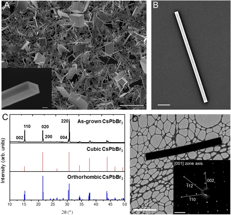
Our initial study focused on CsPbBr3 nanowires, as previous reports suggest this composition is strongly photoluminescent (26, 34) and capable of stimulated emission (29–31). Although we have already reported the synthesis of colloidal CsPbBr3 nanowires (34), those nanowires are too narrow (∼20-nm diameter) to efficiently confine the 535-nm emission and are therefore unable to support photonic lasing (Fig. S1). To achieve lasing, nanowires with diameters greater than ∼180 nm are required, but these are not currently accessible using the colloidal synthesis method. Alternatively, a low-temperature solution-phase process reported by Zhu et al. afforded single-crystal hybrid perovskite (CH3NH3PbX3, X = Cl, Br, I) nanowires and nanoplates with diameters of a few hundred nanometers (20). Inspired by this method, we demonstrate a new solution growth process to synthesize single-crystal CsPbX3 (X = Br, Cl) nanowires and nanoplates by dipping a PbI2 thin film into a CsX–methanol solution with mild heating (50 °C). This method represents, to our knowledge, the first reported synthesis of surfactant-free CsPbX3 nanowires and nanoplates through a simple, low-temperature, solution-phase process. A detailed discussion of the nanowire growth method may be found in the Supporting Information (Fig. S2). From the scanning electron microscopy (SEM) images shown in Fig. 1A, a wide range of CsPbBr3 nanoscale morphologies was produced during the 12-h reaction including nanowires, nanocrystals, and nanoplates. The nanowires range in length from 2 to 40 μm and in width from 0.2 to 2.3 μm, placing them in an ideal size regime for photonic nanowire lasing. The majority of nanowires were found to have rectangular cross-sections (Fig. 1A, Inset) with strongly wire-dependent height-to-width ratios (Fig. S3). Nanowires were chosen for study based on the presence of clean, well-formed facets, which are critical for efficient emission confinement, and transferred by micromanipulator to a clean, fused silica substrate for all optical experiments (Fig. 1B).
Fig. S1.
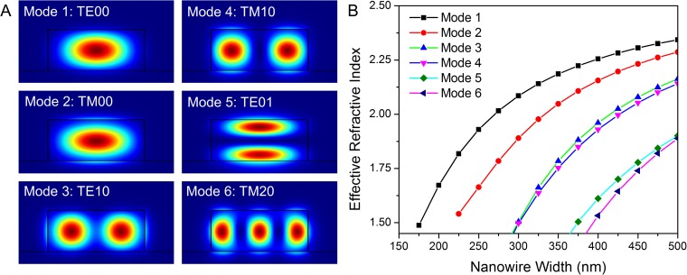
FDE simulations of a CsPbBr3 nanowire. (A) The six sustainable transverse modes for 540-nm light in a CsPbBr3 nanowire with width ≤500 nm. (B) The calculated effective refractive index for each mode as a function of nanowire width. Light is no longer confined to the nanowire once the effective refractive index reaches that of the quartz substrate (n = 1.46). These simulations suggest that a CsPbBr3 nanowire must have a width greater than ∼180 nm to act as an emission waveguide.
Fig. S2.
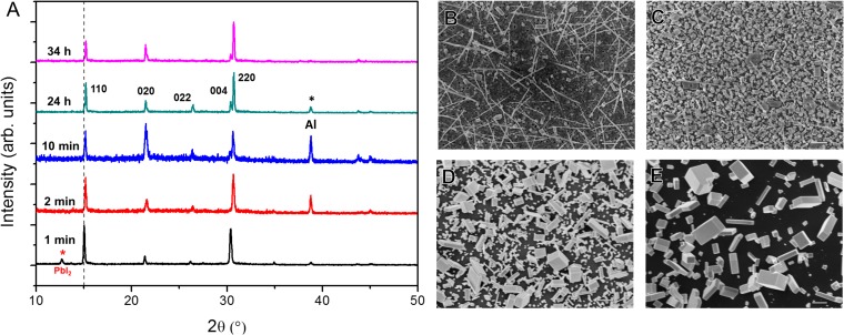
Composition and morphology evolution during nanowire growth at room temperature. (A) XRD patterns at different reaction times. The 24-h pattern is indexed to the CsPbBr3 orthorhombic phase. SEM images at corresponding reaction states: (B) 1 min, (C) 10 min, (D) 24 h, (E) 34 h. (Scale bar, 1 μm.)
Fig. 1.
Structural characterization of single-crystal CsPbBr3 nanowires. (A) SEM images of CsPbBr3 nanowires and nanoplates grown from PbI2 in a methanolic solution of 8 mg/mL CsBr at 50 °C for 12 h. (Scale bar, 10 μm.) (Inset) SEM image of the rectangular end facet of a nanowire. (Scale bar, 500 nm.) (B) A single CsPbBr3 nanowire isolated on a quartz substrate with a 5-nm Au sputter coat. (Scale bar, 1 μm.) (C) XRD pattern of as-grown CsPbBr3 (black) with the standard XRD patterns of cubic (red) and orthorhombic (blue) CsPbBr3. (D) TEM image of an individual nanowire. (Scale bar, 5 μm.) (Inset) SAED pattern from the same nanowire, with relevant crystallographic axes labeled. (Scale bar, 2 nm−1.)
Fig. S3.
CsPbBr3 height and width distribution indicates rectangular cross-sections are favored. Data points determined by AFM (height) and SEM (width).
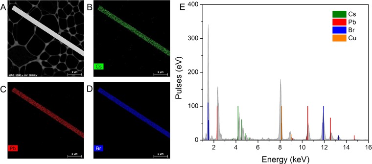
The elemental composition and atomic structure of the nanowires were quantified to ensure they conformed to the expected, room-temperature orthorhombic phase of CsPbBr3. The X-ray diffraction (XRD) pattern of the CsPbBr3 growth substrate shows strong diffraction peaks which can be assigned to the pure orthorhombic crystal structure (space group Pbnm), and does not contain impurity peaks from either the PbI2 or CsBr starting materials (Fig. 1C). The clear splitting of the narrow 002 and 110 peaks further indicates that the as-grown CsPbBr3 is of the room-temperature orthorhombic phase and comprises large, crystalline domains. The nanowire composition was determined by energy-dispersive X-ray spectroscopy, which indicated the presence of Cs, Pb, and Br in a 1.1:1.0:2.7 ratio, in close agreement with the CsPbBr3 phase (Fig. S4). The crystal structure of the nanowires was determined through selected area electron diffraction (SAED) as shown in Fig. 1D. The SAED pattern shown in Fig. 1D (Inset) indicates that the nanowires are single crystalline and may be indexed to the [110] zone axis of the orthorhombic phase of CsPbBr3 in agreement with the XRD pattern. According to the SAED pattern, the nanowire growth direction was also indexed to the [002] direction of the orthorhombic phase of CsPbBr3.
Fig. S4.
Elemental distribution determined from EDS of a single-crystalline CsPbBr3 nanowire. (A) Image of CsPbBr3 nanowire and corresponding (B) Cs, (C) Pb, and (D) Br elemental maps. (E) EDS spectrum from nanowire in A. No detectable levels of iodide were observed indicating the nanowire is not alloyed.
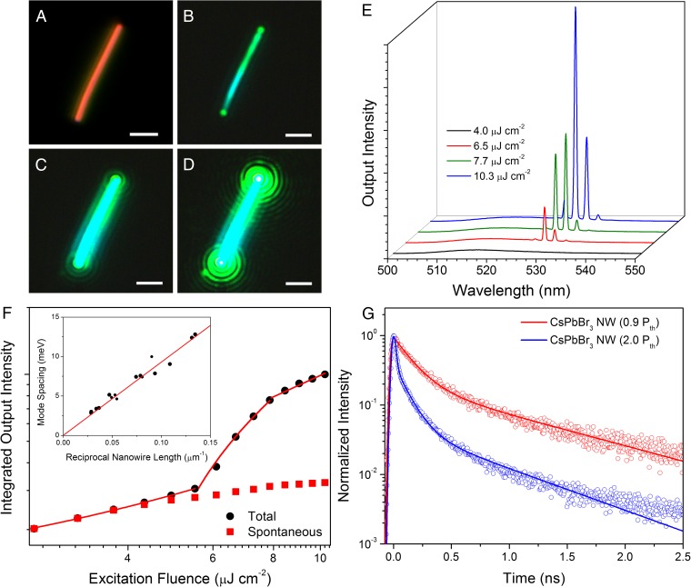
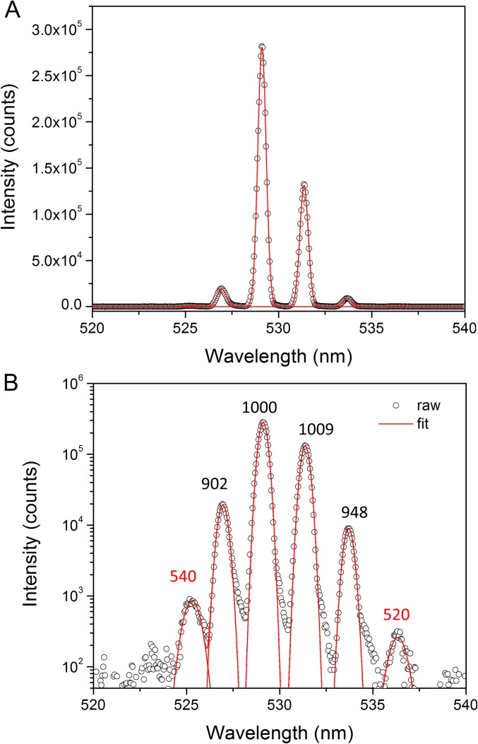
Photonic lasing arises from the unique ability of a nanowire to act as both gain medium and laser cavity. Forming the nanowire from a stable, highly absorptive, and emissive material allows for stimulated emission to occur upon reaching a sufficient carrier density (11, 35). The nanowire geometry defines the laser cavity, which is bounded on either end by the nanowire end facets. The difference in refractive index between the nanowire and its environment (atmosphere, substrate, etc.) generates significant end facet reflectivity as well as efficient wave guiding along the length of the wire. For CsPbBr3 nanowires, lasing was achieved via optical excitation from a femtosecond pulsed laser. At excitation densities below the lasing threshold, spontaneous emission dominates, and the nanowire is uniformly emissive as shown in Fig. 2B. Upon surpassing the threshold, however, stimulated emission takes over and a periodic emission pattern is observed (Fig. 2 C and D), which is caused by interference of the coherent emission from the two end facets of the nanowire. The dependence of the photoluminescence (PL) spectral response on increasing excitation fluence is shown in Fig. 2E. The spontaneous emission from a CsPbBr3 nanowire is centered at 516 nm with a 16-nm (74 meV) FWHM. The spontaneous emission peak first increases with increasing excitation intensity, then plateaus as narrow, closely spaced lasing peaks (0.5-nm minimum FWHM) emerge on the red edge of the emission spectrum near 532 nm and grow rapidly with excitation intensity. The narrow peaks correspond to Fabry–Pérot lasing modes as the mode spacing is found to change linearly with the inverse of the nanowire length (Fig. 2F, Inset). The power-dependent output intensity (Fig. 2F) follows the typical “S”-curve shape and depicts all three PL regimes: spontaneous emission dominates at low excitation intensities until the onset of lasing near 5 μJ cm−2 (Pth), the superlinear PL increase indicative of amplified spontaneous emission follows, and finally gain-pinning and the emergence of lasing occurs past 10 μJ cm−2 (36). The full set of power-dependent spectra is shown in Fig. S5A. Analysis of the individual peak widths from the spectra in Fig. 2E provides information about the nanowire laser cavity quality (Q) factor, or how well the cavity confines and amplifies emission. The Q factor is mode dependent with stronger modes possessing higher values because this corresponds to more efficient amplification and thus higher emission intensity. Using the relationship Q = λ/δλ, where λ is the peak center wavelength and δλ is the peak width, a maximum, single-mode Q factor of 1,009 ± 5 was determined with an average of 960 ± 60 when considering the four major modes (Fig. S6).
Fig. 2.
Lasing in single-crystal CsPbBr3 nanowires. (A) Dark-field image of a CsPbBr3 nanowire. (B–D) The nanowire from A under excitation from a femtosecond pulsed laser with increasing excitation fluence. (Scale bar, 2 µm.) (E) Power-dependent emission spectra from the CsPbBr3 nanowire shown in images A–D. Narrow emission peaks at ∼530 nm are indicative of lasing. (F) The integrated output intensity of the CsPbBr3 nanowire with increasing pump fluence (black circles) follows a typical S-curve pattern and can be linearly fit to show three separate emission regimes: spontaneous emission (<5 µJ cm−2), amplified spontaneous emission (5–10 µJ cm−2), and lasing (>10 µJ cm−2). Spontaneous emission (red squares) from the nanowire plateaus as stimulated emission begins to dominate. (Inset) Plot of inverse nanowire length against mode spacing, confirming that Fabry–Pérot-type lasing is dominant. (G) TRPL from a CsPbBr3 nanowire below (red) and above (blue) the lasing threshold (Pth). The emergence of a rapid decay component (<10 ps) suggests rapid carrier quenching due to stimulated emission.
Fig. S5.
Full PL data from the CsPbBr3 nanowire power-dependent study presented in Fig. 2F. (A) Emission spectra on a log scale, and (B) the peak center of the most intense mode as a function of excitation fluence.
Fig. S6.
Q-factor analysis of a CsPbBr3 nanowire. (A) A linear plot of the emission spectrum at 10.3 µJ cm−2 from Fig. 2E is shown with Gaussian fits of each lasing mode. The spontaneous emission has been subtracted for clarity and ease of fitting. (B) The same spectrum and fit plotted on a log scale showing the quality of the fit. Peak annotations correspond to the Q factor for the specific peak.
Time-resolved PL (TRPL) can be used to measure the carrier population dynamics of the laser cavity above and below the lasing threshold. Below the lasing threshold (Fig. 2G, red trace), the nanowire PL signal decays biexponentially with the rapid component (154 ± 2 ps, 81%) contributing much more than the slower component (970 ± 20 ps, 19%). Based on preliminary TRPL measurements of previously reported, surface-passivated, colloidal CsPbX3 nanowires, which exhibit much longer lifetimes (>>1 ns), we attribute the rapid component to surface state recombination and the longer component to bulk recombination (34). When the excitation fluence is increased past the lasing threshold, an additional decay component is observed (<30 ps, 87%), which decays more rapidly than the other components (110 ± 2 ps, 11%; 720 ± 20 ps, 2%) as well as the instrument response. This rapid decay corresponds to the stimulated emission process depleting carriers that would otherwise undergo spontaneous emission. The low-lasing threshold and high-Q factor place these nanowires in the upper tier of nanowire lasers and clearly demonstrate the effectiveness of CsPbBr3 as a gain medium (see refs. 10, 19, 31 for detailed lists of nanowire lasers and their performance characteristics).
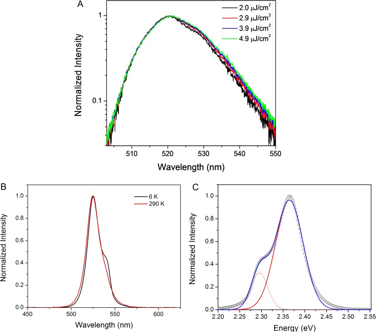
The mechanism for optical gain by stimulated emission in perovskite nanostructures is still under investigation. In CsPbX3 quantum dots, support for both single-exciton and biexciton lasing has been demonstrated (31, 33). In the case of biexciton-driven stimulated emission, a 50-meV red-shifted emission band was assigned to biexciton recombination, in agreement with expected biexciton binding energies in CsPbX3 quantum dots (37). Whereas we observe a similar asymmetric red-shifted emission band at 290 and 6 K (Fig. S7), the red shift of 69 meV is an order of magnitude larger than expected for biexciton binding energies in non-quantum confined CsPbBr3 nanowires. Instead, we postulate that an electron–hole plasma (EHP) mechanism is responsible for stimulated emission, as proposed in well-known compositions such as ZnO (38) and GaN (39) as well as in recent CH3NH3PbX3 nanowires (20). An EHP is formed in bulk crystals when the carrier density surpasses the Mott density; here, the carrier density at the lasing threshold was estimated to be ∼6 × 1017 cm−3 by finite-difference time-domain simulation (Supporting Information), a factor of 3 greater than the bulk CsPbBr3 Mott density of ∼2 × 1017 cm−3. In addition, the formation of an EHP is expected to lead to a blue shift in the cavity modes due to a decrease in the refractive index that arises from exciton absorption saturation (38). We observe a blue shift of 2 nm with increasing excitation fluence (Fig. S5B), suggesting that an EHP mechanism is responsible for stimulated emission in CsPbX3 nanowires. Further study is needed, however, to elucidate the stimulated emission carrier dynamics.
Fig. S7.
Low-energy emission band in CsPbBr3 nanowires. (A) Growth of the low-energy band near 530 nm with increasing femtosecond pulsed excitation fluence. (B) CsPbBr3 nanowire emission at room temperature (290 K) and low temperature (6 K) also shows the growth of the low-energy band. (C) The low-temperature emission spectrum may be fit to a pair of Gaussians (red) that are 69 meV apart.
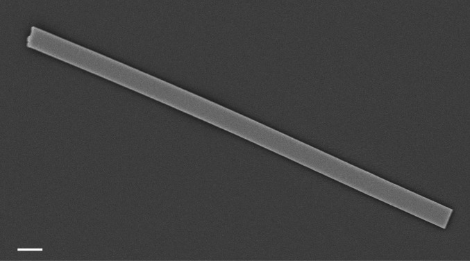
Cesium lead halide materials have been shown to be stable when exposed to atmospheric water or heat, making them attractive for real-world application (27, 33). The CsPbBr3 nanowires reported here are stable for days under ambient atmosphere and illumination without loss of morphology. Additionally, the material composition remains intact over the course of months and does not separate into PbBr2 and other byproducts as has been demonstrated for some hybrid perovskite materials (Fig. 3A) (24). CsPbBr3 nanowires are also stable under constant, pulsed excitation above the lasing threshold. Nanowires were excited to 1.2 Pth under either a closed nitrogen atmosphere or ambient atmosphere (26 °C ± 0.5 °C, 50% ± 1% relative humidity) and the integrated emission intensity was monitored. The results shown in Fig. 3B indicate significant operating lifetimes even under atmospheric conditions. Under nitrogen, nanowire lasing continues uninterrupted for longer than 1 h or over 109 excitation cycles (Fig. 3B, blue trace), with the nanowire undamaged after this time (Fig. S8). Under atmospheric conditions, lasing output is observed to decrease over the course of the experiment, but it does not fall below the original output until over 4.4 × 10⁸ excitation cycles (Fig. 3B, red trace). In contrast, amplified spontaneous emission from thin films of CsPbBr3 falls to 90% after only 1.6 × 10⁷ excitation cycles (31). In hybrid perovskite materials, whispering gallery mode lasing in CH3NH3PbI3 persists for 8 × 10⁶ excitation cycles (40), whereas the long-term lasing stability of CH3NH3PbX3 nanowires lasers has not been reported (20). The stable, continuous lasing operation observed here is promising for future applications as it suggests both high photo- and thermal stability under ideal or suboptimal environmental conditions.
Fig. 3.
Stability of CsPbBr3. (A) XRD patterns of as-grown CsPbBr3 before testing (black), after exposure to air for 2 mo (red), and after annealing at 200 °C (blue). In both cases, the CsPbBr3 phase remained identical to the as-grown and indicated high compositional stability. (B) Integrated emission intensity for CsPbBr3 nanowires under constant pulsed excitation (1.2 Pth) while exposed to nitrogen (blue) and ambient atmosphere (red).
Fig. S8.
SEM image of CsPbBr3 nanowire after 1 h of continuous pulsed excitation above the lasing threshold while under nitrogen. (Scale bar, 1 μm.)
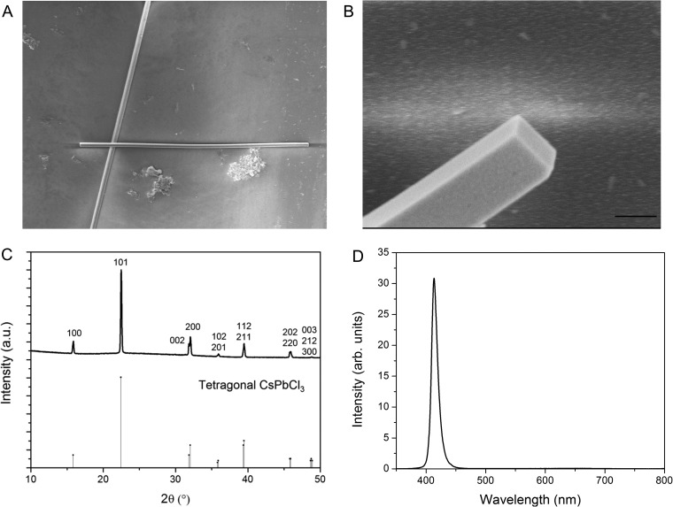
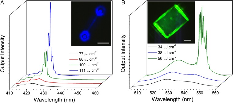
Lasing is also possible for other CsPbX3 compositions and geometries besides CsPbBr3 nanowires. Single-crystal nanowires of CsPbCl3 were successfully synthesized by replacing CsBr with CsCl during the reaction, with the XRD pattern confirming the expected tetragonal phase of the as-grown CsPbCl3 (see Fig. S9 for characterization). The smooth, rectangular facets of the CsPbCl3 nanowires, as well as the strong PL emission centered at 418 nm, make them ideal for extending the wavelength range of CsPbX3 nanowire lasers. Upon focused excitation, lasing occurred near 430 nm with the emergence of narrow peaks similar to CsPbBr3 nanowires as shown in Fig. 4A. The lasing threshold was found at ∼86 μJ cm−2, significantly higher than for CsPbBr3 nanowires, and the Q factor was consequently found to be lower, with a maximum of 690 ± 70 and an average of 580 ± 120. Nevertheless, interference from end facet emission was observed (Fig. 4A, Inset), indicating effective waveguiding and coherent emission from the nanowire. Halide alloying may be pursued in the future to achieve broad wavelength tunability as observed in CsPbX3 quantum dots and CH3NH3PbX3 materials (20, 41). In addition to nanowires, well-faceted CsPbBr3 nanoplates were found to lase at ∼38 μJ cm−2 with the power-dependent emission spectra shown in Fig. 4B. Despite the high mode density, peak fitting yields a mode spacing of 3.9 ± 0.7 meV (Fig. S10), which for a 19.3-μm-long plate falls within error of the fit line shown in Fig. 3E (Inset). This suggests Fabry–Pérot lasing from multiple transverse modes, which may be easily supported by the broad, rectangular plate. This assignment is further supported by the stronger emission intensity observed at one pair of end facets indicating a preference for lasing in that direction (Fig. 4B, Inset). This lasing behavior is in contrast to whispering gallery mode lasing observed in 100-μm-sized plates of CsPbBr3, which demonstrated broad peak spacing and a uniform spatial emission profile (31).
Fig. S9.
Characterization of as-grown CsPbCl3 nanowires. (A) SEM image of an individual CsPbCl3 nanowire. (Scale bar, 5 μm.) (B) Magnified SEM image depicting rectangular end facets. (Scale bar,1 μm.) (C) XRD pattern of the growth substrate indexed to the tetragonal phase of CsPbCl3. (D) Narrow PL emission centered at 418 nm observed from a single CsPbCl3 nanowire.
Fig. 4.
Lasing in CsPbCl3 nanowires and CsPbBr3 nanoplates. (A) CsPbCl3 nanowire power-dependent emission spectra showing lasing at ∼425 nm. (Inset) Optical image of the same nanowire above the lasing threshold. (Scale bar, 5 μm.) (B) CsPbBr3 nanoplate power-dependent emission spectra showing lasing at ∼545 nm. (Inset) Optical image of the same nanoplate above the lasing threshold. (Scale bar, 5 μm.)
Fig. S10.
PL spectrum of the CsPbBr3 nanoplate in Fig. 4B at 56 μJ cm−2 fit to 12 Gaussian functions. The spontaneous emission has been subtracted for clarity and ease of fitting. The mode spacing suggests Fabry–Pérot-type lasing.
Here we have reported, to our knowledge, the first successful demonstration of lasing in cesium lead halide nanowires. A facile synthetic procedure was optimized to yield a range of CsPbBr3 nanowires and nanoplates, both of which were found to lase. CsPbBr3 nanowires exhibited low lasing thresholds and relatively high Q factors compared with the field. Most strikingly, the nanowires were stable under both ambient conditions as well as during continuous lasing, important benchmarks for application. Wavelength tunability was also demonstrated through halide substitution, and our ongoing study of anionic alloying indicates the possibility of even greater wavelength tunability across the entire visible spectral range. Overall, we have shown that cesium lead halide nanowires are versatile, stable platforms for future nanophotonic exploration and development.
Materials and Methods
Additional details regarding the materials and methods may be found in the Supporting Information.
Synthesis of CsPbX3 Nanowires and Nanoplates.
All of the chemicals were purchased from Sigma-Aldrich and used as received unless otherwise stated. Poly(3,4-ethylenedioxythiophene) polystyrene sulfonate (PEDOT:PSS)-coated glass substrates were prepared by cutting ∼1 × 1-cm glass substrates and washing sequentially with acetone, isopropanol, and deionized water. Cleaned substrates were then O2-plasma-treated for 10 min, followed by spin coating with PEDOT:PSS (Solarmer) at 3,000 rpm for 30 s. Afterward, the coated substrates were annealed at 150 °C for 15 min.
To grow CsPbX3 nanowires and nanoplates, 460 mg PbI2 (99.999%) was dissolved in 1 mL anhydrous dimethylformamide and stirred at 70 °C overnight before further use. The PbI2 solution was spun onto the PEDOT:PSS-coated glass substrates at 1,000 rpm for 120 s, then annealed at 100 °C for 15 min. The PbI2 film was carefully submerged into a glass vial with 8 mg/mL CsBr (99.999%) solution in methanol (anhydrous, 99.8%), with the PbI2 side facing up. The capped reaction vial was heated at 50 °C for 12 h, and the substrate was removed and washed in anhydrous isopropanol for 30 s. The sample was then dried by heating to 50 °C for 5 min. For the synthesis of CsPbCl3 nanowires, the CsBr–methanol solution was replaced with a 6 mg/mL CsCl–methanol solution. The entire growth process was carried out in a nitrogen-filled glove box.
SEM measurements.
SEM images were obtained using a JEOL JSM-6340F field-emission SEM. To acquire SEM images of nanowires on fused silica, the substrates were sputter coated with 5-nm gold using a Denton Vacuum Desk IV sputtering system.
XRD measurements.
Powder XRD was measured using a Bruker AXS D8 Advance diffractometer with a Cu Kα source.
Transmission electron microscopy and SAED measurements.
Characterization of the nanowires by electron diffraction and low-resolution transmission electron microscopy (TEM) was conducted using an FEI Tecnai TEM operating at an accelerating voltage of 200 kV.
PL and TRPL measurements.
Individual wires were transferred to fused silica coverslips and secured in N2-gas-filled cells for all optical measurements, unless otherwise noted. The cells were mounted in a modified Olympus IX71 inverted confocal microscope, equipped with a 2D piezoelectric scanning stage. The second harmonic of the output of a Coherent RegA amplifier (800 nm, 150–200 fs, 295 kHz) seeded by a Coherent Mira oscillator was used as the 400 ± 3-nm excitation light. The 400-nm light was focused to a spot size of 29 ± 4 μm to uniformly illuminate single nanowires using a 50× 0.50-N.A. air objective (Olympus LMPLFLN). Emission from the wires was collected in an epifluorescence scheme; optical wide-field images were taken with an AxioCam MRc5 CCD, while spectra were acquired with a fiber coupled UV-vis spectrometer (Acton Spectra Pro-300i, 1,200 mm−1, 300-nm blaze) equipped with a liquid-N2-cooled CCD (Roper Scientific 7346–0001). The spectral resolution was 0.06 nm. Lifetime measurements were performed using two avalanche photodiodes (Micro Photon Devices PDM-50 series) input to a time-correlated single-photon counting module (PicoQuant PicoHarp 300/PHR 800) with an instrument response of ∼30 ps. All lasing experiments were conducted at room temperature (26 °C).
Additional Characterization and Simulation of CsPbX3 Nanowires and Plates
Atomic Force Microscopy Measurements.
Atomic force microscopy (AFM) images of the nanowires were acquired using an Asylum MFP 3D in tapping mode.
Energy-Dispersive Spectroscopy Measurements.
Quantification of the elemental ratios in a CsPbBr3 was studied using an FEI Titan microscope operated at 200 kV at the National Center for Electron Microscopy in the Molecular Foundry at Lawrence Berkeley National Laboratory. Signal was collected using an FEI Super-X Quad windowless detector based on silicon drift technology controlled by Bruker Esprit software.
Low-Temperature PL Measurements.
Samples were held under vacuum (5 × 10⁻⁶ torr) in a Janis Research Co. ST-500 microscopy cryostat and cooled to 6 K with liquid helium. The samples were excited with the fourth harmonic (266 nm) of a Spectra-Physics Quanta Ray INDI-40 neodymium-doped yttrium aluminum garnet laser (10-Hz, 8-ns pulse width). The PL emission was collected by a 50×, 0.55-N.A. air objective (Nikon CF Plan) and the spectra were measured with the same UV-vis spectrometer as described in Materials and Methods, but using a 150-mm−1, 300-nm blaze grating.
CsPbBr3 Refractive Index Calculations.
The calculations were based on density functional theory (42) within the generalized gradient approximation formulated by Perdew, Burke, and Ernzerhof (43) as implemented in the Vienna ab initio simulation package (VASP) code (44). The projector augmented wave pseudopotentials were used (45), and the valence wavefunctions were expanded using a plane-wave basis with an energy cutoff of 300 eV. A primitive cell of CsPbBr3 (20 atoms) in the orthorhombic phase was used (26), and the Brillouin zone was sampled with a 7 × 7 × 5 k-point mesh. To calculate the frequency-dependent dielectric function, 200 empty bands were used. The calculated static dielectric constant (ω = 0) agrees with the result from the density functional perturbation theory calculation implemented in VASP. The frequency-dependent dielectric function was used to calculate the refractive indices, using the equations (46)
| [1] |
| [2] |
where n and ε1 are the real parts of the refractive index and relative dielectric constant, respectively, k and ε2 are the imaginary parts of the refractive index and relative dielectric constant, respectively, and all are a function of the frequency, ν. The resulting refractive index values were used directly for the finite-difference eigenmode and finite-difference time-domain simulations below. Graphs of the real and imaginary refractive indices may be found in Fig. S11.
Fig. S11.
Frequency-dependent refractive indices for the orthorhombic phase of CsPbBr3. (A) Real and (B) imaginary parts of the refractive index.
Finite-Difference Eigenmode Simulations.
The Lumerical MODE Solutions 7.6 software package was used to simulate the waveguide modes of 535-nm light in a CsPbBr3 nanowire. The nanowire (n = 2.53) was simulated on fused silica (n = 1.46) (47) under vacuum (n = 1.00). The side length ratio was kept at 2:1 to approximate the rectangular cross-section of the as-grown nanowires. The nanowire size was incremented by 25 nm (based on width), and the effective refractive index was calculated for all sustainable modes.
Finite-Difference Time-Domain Simulations.
The Lumerical FDTD Solutions 8.12 software package was used to estimate the absorption cross-section of the 483 nm × 265 nm × 11.1-μm CsPbBr3 nanowire studied in Fig. 2. As in the finite-difference eigenmode (FDE) mode simulation, the nanowire was simulated laying horizontal on fused silica surrounded by vacuum. The 400-nm total-field scattered-field light source was positioned above the nanowire and the transverse electric and transverse magnetic polarizations averaged to acquire the absorption cross-section. Combined with the excitation fluence and beam profile, the nanowire carrier density was determined.
Discussion of the Nanowire and Nanoplate Growth Mechanism
During the initial stages of the reaction using 6–10 mg/mL CsBr in methanol, the film color transitioned rapidly to red, then gradually to yellow. We hypothesize that an intermediate CsPbIxBr3−x forms initially, then evolves to pure CsPbBr3 as confirmed by XRD patterns at different growth times (Fig. S2). The peaks corresponding to PbI2 disappear within the first 2 min, indicating that PbI2 dissolves/reacts rapidly. For the intermediate products from 2–10 min, the (001) peak was shifted ∼0.2° below that of pure CsPbBr3; this is indicative of lattice expansion caused by the formation of CsPbIxBr3−x. However, the final CsPbBr3 nanowires produced by this method contain a minimal amount of iodide as the iodide content of the nanowires tested by energy-dispersive spectroscopy (EDS) was found to be below the 1% detection limit of the instrument. Notably, Zhu et al. reported intermediate CH3NH3PbI2Br products during the growth of single-crystal CH3NH3PbBr3 nanostructures (20). Therefore, inorganic perovskite nanowires likely possess similar growth dynamics to hybrid perovskites.
Acknowledgments
This work was supported by the US Department of Energy (DOE) under Contract DE-AC02-05CH11231 (PChem KC3103). Transmission electron microscopy (TEM) characterization was carried out at the National Center for Electron Microscopy and Molecular Foundry. Work at the Molecular Foundry was supported by the Office of Science, Office of Basic Energy Sciences, of the DOE under Contract DE-AC02-05CH11231. S.W.E. thanks the Camille and Henry Dreyfus Foundation for funding, Award EP-14-151. M.L. thanks Suzhou Industrial Park for the fellowship support. J.M. and L.-W.W. thank the support of the Joint Center for Artificial Photosynthesis funded by DOE (DE-SC0004993).
Footnotes
The authors declare no conflict of interest.
This article contains supporting information online at www.pnas.org/lookup/suppl/doi:10.1073/pnas.1600789113/-/DCSupplemental.
References
- 1.Beausoleil RG, Kuekes PJ, Snider GS, Shih-Yuan W, Williams RS. Nanoelectronic and nanophotonic interconnect. Proc IEEE. 2008;96(2):230–247. [Google Scholar]
- 2.Miller DAB. Device requirements for optical interconnects to silicon chips. Proc IEEE. 2009;97(7):1166–1185. [Google Scholar]
- 3.Yan R, et al. Nanowire-based single-cell endoscopy. Nat Nanotechnol. 2012;7(3):191–196. doi: 10.1038/nnano.2011.226. [DOI] [PubMed] [Google Scholar]
- 4.Nakayama Y, et al. Tunable nanowire nonlinear optical probe. Nature. 2007;447(7148):1098–1101. doi: 10.1038/nature05921. [DOI] [PubMed] [Google Scholar]
- 5.Pan L, Bogy DB. Data storage: Heat-assisted magnetic recording. Nat Photonics. 2009;3(4):189–190. [Google Scholar]
- 6.Huang MH, et al. Room-temperature ultraviolet nanowire nanolasers. Science. 2001;292(5523):1897–1899. doi: 10.1126/science.1060367. [DOI] [PubMed] [Google Scholar]
- 7.Chu S, et al. Electrically pumped waveguide lasing from ZnO nanowires. Nat Nanotechnol. 2011;6(8):506–510. doi: 10.1038/nnano.2011.97. [DOI] [PubMed] [Google Scholar]
- 8.Li KH, Liu X, Wang Q, Zhao S, Mi Z. Ultralow-threshold electrically injected AlGaN nanowire ultraviolet lasers on Si operating at low temperature. Nat Nanotechnol. 2015;10(2):140–144. doi: 10.1038/nnano.2014.308. [DOI] [PubMed] [Google Scholar]
- 9.Li KH, Liu X, Wang Q, Zhao S, Mi Z. An electrically injected AlGaN nanowire laser operating in the ultraviolet-C band. Appl Phys Lett. 2015;107(4):043101. [Google Scholar]
- 10.Ding K, et al. Record performance of electrical injection sub-wavelength metallic-cavity semiconductor lasers at room temperature. Opt Express. 2013;21(4):4728–4733. doi: 10.1364/OE.21.004728. [DOI] [PubMed] [Google Scholar]
- 11.Couteau C, Larrue A, Wilhelm C, Soci C. Nanowire lasers. Nanophotonics. 2015;4(1):90–107. [Google Scholar]
- 12.Eperon GE, Burlakov VM, Docampo P, Goriely A, Snaith HJ. Morphological control for high performance, solution-processed planar heterojunction perovskite solar cells. Adv Funct Mater. 2014;24(1):151–157. [Google Scholar]
- 13.Jeon NJ, et al. Solvent engineering for high-performance inorganic-organic hybrid perovskite solar cells. Nat Mater. 2014;13(9):897–903. doi: 10.1038/nmat4014. [DOI] [PubMed] [Google Scholar]
- 14.Liu D, Kelly TL. Perovskite solar cells with a planar heterojunction structure prepared using room-temperature solution processing techniques. Nat Photonics. 2014;8(2):133–138. [Google Scholar]
- 15.Zhou H, et al. Interface engineering of highly efficient perovskite solar cells. Science. 2014;345(6196):542–546. doi: 10.1126/science.1254050. [DOI] [PubMed] [Google Scholar]
- 16.Tan Z-K, et al. Bright light-emitting diodes based on organometal halide perovskite. Nat Nanotechnol. 2014;9(9):687–692. doi: 10.1038/nnano.2014.149. [DOI] [PubMed] [Google Scholar]
- 17.Kim Y-H, et al. Multicolored organic/inorganic hybrid perovskite light-emitting diodes. Adv Mater. 2015;27(7):1248–1254. doi: 10.1002/adma.201403751. [DOI] [PubMed] [Google Scholar]
- 18.Dou L, et al. Solution-processed hybrid perovskite photodetectors with high detectivity. Nat Commun. 2014;5:5404. doi: 10.1038/ncomms6404. [DOI] [PubMed] [Google Scholar]
- 19.Lin Q, Armin A, Lyons DM, Burn PL, Meredith P. Low noise, IR-blind organohalide perovskite photodiodes for visible light detection and imaging. Adv Mater. 2015;27(12):2060–2064. doi: 10.1002/adma.201405171. [DOI] [PubMed] [Google Scholar]
- 20.Zhu H, et al. Lead halide perovskite nanowire lasers with low lasing thresholds and high quality factors. Nat Mater. 2015;14(6):636–642. doi: 10.1038/nmat4271. [DOI] [PubMed] [Google Scholar]
- 21.Xing J, et al. Vapor phase synthesis of organometal halide perovskite nanowires for tunable room-temperature nanolasers. Nano Lett. 2015;15(7):4571–4577. doi: 10.1021/acs.nanolett.5b01166. [DOI] [PubMed] [Google Scholar]
- 22.Zhang Q, Ha ST, Liu X, Sum TC, Xiong Q. Room-temperature near-infrared high-Q perovskite whispering-gallery planar nanolasers. Nano Lett. 2014;14(10):5995–6001. doi: 10.1021/nl503057g. [DOI] [PubMed] [Google Scholar]
- 23.Niu G, Guo X, Wang L. Review of recent progress in chemical stability of perovskite solar cells. J Mater Chem A Mater Energy Sustain. 2015;3(17):8970–8980. [Google Scholar]
- 24.Conings B, et al. Intrinsic thermal instability of methylammonium lead trihalide perovskite. Adv Energy Mater. 2015;5(15):1500477. [Google Scholar]
- 25.Lee J-W, et al. Formamidinium and cesium hybridization for photo- and moisture-stable perovskite solar cell. Adv Energy Mater. 2015;5(20):1501310. [Google Scholar]
- 26.Stoumpos CC, et al. Crystal growth of the perovskite semiconductor CsPbBr3: A new material for high-energy radiation detection. Cryst Growth Des. 2013;13(7):2722–2727. [Google Scholar]
- 27.Kulbak M, Cahen D, Hodes G. How important is the organic part of lead halide perovskite photovoltaic cells? Efficient CsPbBr3 cells. J Phys Chem Lett. 2015;6(13):2452–2456. doi: 10.1021/acs.jpclett.5b00968. [DOI] [PubMed] [Google Scholar]
- 28.Somma F, Nikl M, Nitsch K, Fabeni P, Pazzi GP. Excitons in CsPbX3 (X=Cl, Br, I) ternary nanocrystallites in thin film matrices. J Lumin. 2001;94–95(0):169–172. [Google Scholar]
- 29.Kondo S, Saito T, Asada H, Nakagawa H. Stimulated emission from microcrystalline CsPbBr3 films: Edge emission versus surface emission. Mater Sci Eng B. 2007;137(1–3):156–161. [Google Scholar]
- 30.Kondo S, et al. High intensity photoluminescence of microcrystalline CsPbBr3 films: Evidence for enhanced stimulated emission at room temperature. Curr Appl Phys. 2007;7(1):1–5. [Google Scholar]
- 31.Yakunin S, et al. Low-threshold amplified spontaneous emission and lasing from colloidal nanocrystals of caesium lead halide perovskites. Nat Commun. 2015;6:8056. doi: 10.1038/ncomms9056. [DOI] [PMC free article] [PubMed] [Google Scholar]
- 32.Protesescu L, et al. Nanocrystals of cesium lead halide perovskites (CsPbX₃, X = Cl, Br, and I): Novel optoelectronic materials showing bright emission with wide color gamut. Nano Lett. 2015;15(6):3692–3696. doi: 10.1021/nl5048779. [DOI] [PMC free article] [PubMed] [Google Scholar]
- 33.Wang Y, et al. All-inorganic colloidal perovskite quantum dots: A new class of lasing materials with favorable characteristics. Adv Mater. 2015;27(44):7101–7108. doi: 10.1002/adma.201503573. [DOI] [PubMed] [Google Scholar]
- 34.Zhang D, Eaton SW, Yu Y, Dou L, Yang P. Solution-phase synthesis of cesium lead halide perovskite nanowires. J Am Chem Soc. 2015;137(29):9230–9233. doi: 10.1021/jacs.5b05404. [DOI] [PubMed] [Google Scholar]
- 35.Ma Y, Guo X, Wu X, Dai L, Tong L. Semiconductor nanowire lasers. Adv Opt Photonics. 2013;5(3):216–273. [Google Scholar]
- 36.Zimmler MA, Bao J, Capasso F, Müller S, Ronning C. Laser action in nanowires: Observation of the transition from amplified spontaneous emission to laser oscillation. Appl Phys Lett. 2008;93(5):051101. [Google Scholar]
- 37.Klimov VI. Spectral and dynamical properties of multiexcitons in semiconductor nanocrystals. Annu Rev Phys Chem. 2007;58(1):635–673. doi: 10.1146/annurev.physchem.58.032806.104537. [DOI] [PubMed] [Google Scholar]
- 38.Johnson JC, Yan H, Yang P, Saykally RJ. Optical cavity effects in ZnO nanowire lasers and waveguides. J Phys Chem B. 2003;107(34):8816–8828. [Google Scholar]
- 39.Johnson JC, et al. Single gallium nitride nanowire lasers. Nat Mater. 2002;1(2):106–110. doi: 10.1038/nmat728. [DOI] [PubMed] [Google Scholar]
- 40.Sutherland BR, Hoogland S, Adachi MM, Wong CTO, Sargent EH. Conformal organohalide perovskites enable lasing on spherical resonators. ACS Nano. 2014;8(10):10947–10952. doi: 10.1021/nn504856g. [DOI] [PubMed] [Google Scholar]
- 41.Nedelcu G, et al. Fast anion-exchange in highly luminescent nanocrystals of cesium lead halide perovskites (CsPbX3, X = Cl, Br, I) Nano Lett. 2015;15(8):5635–5640. doi: 10.1021/acs.nanolett.5b02404. [DOI] [PMC free article] [PubMed] [Google Scholar]
- 42.Kohn W, Sham LJ. Self-consistent equations including exchange and correlation effects. Phys Rev. 1965;140(4A):A1133–A1138. [Google Scholar]
- 43.Perdew JP, Burke K, Ernzerhof M. Generalized gradient approximation made simple. Phys Rev Lett. 1996;77(18):3865–3868. doi: 10.1103/PhysRevLett.77.3865. [DOI] [PubMed] [Google Scholar]
- 44.Kresse G, Furthmüller J. Efficiency of ab-initio total energy calculations for metals and semiconductors using a plane-wave basis set. Comput Mater Sci. 1996;6(1):15–50. [Google Scholar]
- 45.Kresse G, Joubert D. From ultrasoft pseudopotentials to the projector augmented-wave method. Phys Rev B: Condens Matter. 1999;59(3):1758–1775. [Google Scholar]
- 46.Fox M. Introduction. Optical Properties of Solids. Oxford Univ Press; New York: 2001. pp. 1–20. [Google Scholar]
- 47.Malitson IH. Interspecimen comparison of the refractive index of fused silica. J Opt Soc Am. 1965;55(10):1205–1209. [Google Scholar]


