Abstract
Thermoelectric technology, which possesses potential application in recycling industrial waste heat as energy, calls for novel high-performance materials. The systematic exploration of novel thermoelectric materials with excellent electronic transport properties is severely hindered by limited insight into the underlying bonding orbitals of atomic structures. Here we propose a simple yet successful strategy to discover and design high-performance layered thermoelectric materials through minimizing the crystal field splitting energy of orbitals to realize high orbital degeneracy. The approach naturally leads to design maps for optimizing the thermoelectric power factor through forming solid solutions and biaxial strain. Using this approach, we predict a series of potential thermoelectric candidates from layered CaAl2Si2-type Zintl compounds. Several of them contain nontoxic, low-cost and earth-abundant elements. Moreover, the approach can be extended to several other non-cubic materials, thereby substantially accelerating the screening and design of new thermoelectric materials.
 Thermoelectric materials with enhanced performances need to be identified. Here, the authors use the crystal field splitting energy of orbitals as a descriptor to design thermoelectric materials by solid solution maps and strain engineering in layered CaAl2Si2-type Zintl compounds.
With the gradual depletion of fossil fuels and the growing pressure of the global warming, developing reliable and sustainable approaches for energy conversion is a key challenge for our society. Thermoelectric (TE) devices, which can directly and reversibly convert heat into electricity, have potential applications in waste-heat recovery, air conditioning and refrigeration1,2. However, the application of TE devices is critically limited by their low efficiencies, which are determined by the performance of the materials. Numerous efforts worldwide thus focus on optimizing current TE materials and developing novel TE materials with enhanced performance3,4,5,6,7,8,9. The performance of TE materials is governed by the dimensionless figure of merit, zT=α2σT/κ, where α is the Seebeck coefficient, σ is the electrical conductivity, κ is the thermal conductivity and T is the absolute temperature. Accordingly, enhanced zT value requires a combination of excellent electrical transport properties, quantified by the TE power factor PF=α2σ, and low thermal conductivity.
Several successful concepts, including nano-structuring10 and the inclusion of loosely bound rattlers11, have been developed to systematically reduce the lattice thermal conductivity. On the other hand, a systematic optimization of the electronic properties, which often exhibit a highly nontrivial dependence on atomic structure, still poses a big challenge. High-throughput computational screening allows the identification of compounds with high power factors via electronic transport calculations12,13. The physical insight from the approach is, however, mainly limited to the rationalization of the calculated properties. Furthermore, derived compounds, for example, a high-performing alloy of two low-performing compounds, can be overlooked. How alloying can optimize the PF by alignment of band edges has been demonstrated experimentally5,14,15 and theoretically16,17. However, despite the intuitive appeal of this approach, it has only been applied to a few cubic or pseudo-cubic alloys. This might be attributed to the limited insight into the underlying bonding orbitals at the band edges, which makes it difficult to extend the approach to new materials.
Here, taking layered CaAl2Si2-type Zintl compounds as an example, we combine first principles calculations and reported experimental data18,19,20,21,22,23,24,25,26,27,28,29,30,31,32,33 to demonstrate how the TE properties can be rationalized in terms of a simple crystal field scheme of orbitals splitting. Thereby, a powerful selection rule only based on band structure parameters is established as a simplified descriptor of electrical transport performance. Using the screening rule, we identify a few promising TE candidates with nontoxic, inexpensive and earth-abundant elements from CaAl2Si2-type Zintl compounds. It is shown how the selection rule naturally leads to strategies for rationally optimizing the TE PF through solid solution map and biaxial strain engineering. Finally, the strategy is reasonably extended to several other types of materials including chalcopyrite, metal dichalcogenide and lithium intercalated metal dichalcogenide. The orbital engineering approach presented here thus provides insightful guidance for the search and design of novel promising TE materials with good electronic transport properties.
Results
Orbital characteristics and electronic transport properties
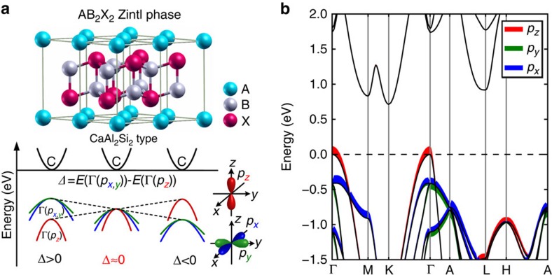
AB2X2 Zintl compounds crystallize in trigonal (space group: P m1) CaAl2Si2-type structures, where A is an alkaline-earth or a divalent rare-earth element, B is a transition-metal or a main group element, X normally comes from group 15 and 14 (ref. 34). Generally, layered AB2X2 Zintl compounds can be described as trigonal monolayers of A2+ cations in the a-b plane separating [B2X2]2− covalently bound slabs (Fig. 1a)27. These Zintl compounds are known by the virtue of low thermal conductivity35. Furthermore, the wide variety of compositions covered by this type of compounds provides considerable chemical tunability of the transport properties. However, their complicated chemical bonds, described in detail in ref. 34, make it a big challenge to systematically optimize the electronic transport properties.
Figure 1. Orbital engineering to realize threefold degenerate p orbitals in layered CaAl2Si2-type Zintl compounds.
(a) Crystal structure and electronic bands of CaAl2Si2-type Zintl compounds. Nondegenerate band Γ(pz) and doubly degenerate band Γ(px,y) are mainly composed of pz and px,y orbitals from anions, respectively. Δ is the crystal field splitting energy between px,y and pz orbitals at the Γ point. (b) Orbital-projected band structure of representative CaAl2Si2-type Zintl compound Mg3Sb2 with negative Δ value. px, py and pz orbitals of Sb anions are projected on the band structure. Curve width indicates the relative weight of the component. Two representative compounds Mg3Sb2 (Δ<0) and SrZn2Sb2 (Δ>0, Supplementary Fig. 2) are used to demonstrate the p orbital characteristics of CaAl2Si2-type Zintl materials.
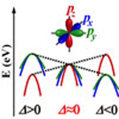
The basic idea of the present paper is illustrated in Fig. 1a. The AB2X2 Zintl compounds are intrinsically p-doped36 and the electronic transport properties depend sensitively on the degeneracy of the valence band edges around the Brillouin zone centre at the Γ point. The valence band edge is dominated by the p orbital characteristics of the X anions (see Fig. 1b and Supplementary Figs 1 and 2 for details). Cubic symmetry would result in threefold degenerate p orbitals at Γ point because of the equivalency of the x, y, z directions in the Brillouin zone. However, owing to the effect of the crystal field splitting (see Supplementary Note 1 for details. The effect of spin orbit coupling is discussed in Supplementary Note 2.), the pz orbital is separated from the px and py orbitals in layered materials. As a result, the valence bands at the Γ point split into a doubly degenerate band Γ(px,y) and a nondegenerate band Γ(pz), mainly composed, respectively, of px,y and pz orbitals from anions (Fig. 1). The energy difference between these two bands is defined as the crystal field splitting energy, namely, Δ=E(Γ(px,y))−E(Γ(pz)). In general, Γ(px,y) is a heavy hole band, whereas Γ(pz) is a light hole band. It is desirable for optimizing electrical transport performance that Γ(px,y) band and Γ(pz) band are nearly degenerate5,15,16. Thus, the magnitude of Δ (|Δ|) can be used to evaluate the deviation from cubic-like threefold degeneracy of p orbitals at the band edges and thereby electrical transport properties. The deviation decreases as |Δ| gets smaller, and orbital degeneracy is effectively increased when Δ value is around zero. Therefore, orbital engineering is here understood as the reconstruction of cubic-like threefold degenerate p orbitals at the band edges in layered compounds through the manipulation of the relative energies of px, py and pz orbitals (see Fig. 1a for details).
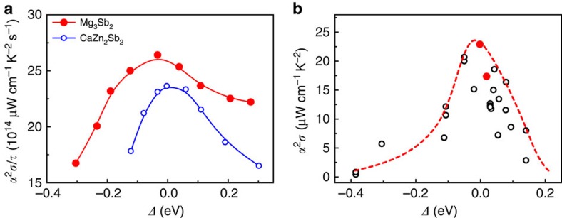
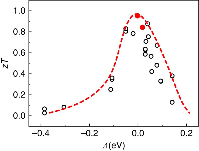
Figure 2a shows the calculated dependence of the PF on Δ for two representative CaAl2Si2-type Zintl compounds Mg3Sb2 and CaZn2Sb2 with, respectively, negative and positive Δ values (see also Supplementary Figs 3a, 4 and 5 for details). The theoretical power factors increase with the increasing Δ value and then decrease, showing peak values when Δ approaches zero, which is consistent with the above discussion. Figure 2b (see also Supplementary Fig. 3b for details) shows the experimental power factors of all reported TE Zintl compounds18,19,20,21,22,23,24,25,26,27,28,29,30,31,32,33 with the CaAl2Si2-type structure and their correlation with the calculated Δ. The result confirms that the peak power factors are obtained as Δ≈0, fully consistent with the trend of theoretical power factors. Moreover, the tendency of the experimental zT values at different temperatures shown in Fig. 3 and Supplementary Fig. 6 strongly resembles the dependence of the power factors on Δ. Considerably enhanced zT values are observed when Δ is around zero. In a few reported CaAl2Si2-type Zintl compounds with nearly zero Δ values, the optimum zT values18,19 of 1.0–1.2 are achieved at the temperature range of 600–700 K.
Figure 2. The dependence of thermoelectric power factors on crystal field splitting energy.
(a) Calculated power factors α2σ/τ at 600 K of two representative CaAl2Si2-type Zintl compounds, Mg3Sb2 and CaZn2Sb2, with negative and positive Δ, respectively. The crystal field splitting energy Δ is varied by slightly tuning lattice parameters a and c. For each Δ value, the theoretical power factor α2σ/τ is calculated at a hole concentration p=1020 cm−3. A similar dependence of α2σ/τ on Δ is observed if the optimal carrier concentration is used (Supplementary Fig. 5). The solid lines represent fitted curves using a B spline. τ is the constant carrier relaxation time. (b) Experimental power factors18,19,20,21,22,23,24,25,26,27,28,29,30,31,32,33 α2σ at 600 K as a function of the crystal field splitting energy Δ in CaAl2Si2-type Zintl compounds. Solid solutions YbCd1.6Zn0.4Sb2 and EuZn1.8Cd0.2Sb2 with zT values18,19 above unity are marked in red. Experimental reported Zintl compounds18,19,20,21,22,23,24,25,26,27,28,29,30,31,32,33 studied here include YbCd2Sb2, YbZn2Sb2, EuZn2Sb2, EuCd2Sb2, CaZn2Sb2, SrZn2Sb2, CaMg2Bi2, YbMg2Bi2, Mg3Bi2, Mg3Sb2, Eu(Zn1−xCdx)2Sb2 (x=0.1, 0.3 and 0.5), Yb(Zn1−xCdx)2Sb2 (x=0.5 and 0.8) and Yb1−xEuxCd2Sb2 (x=0.25). The curve is guide to the eye, showing the best values corresponding to optimum carrier concentrations. The data points include varying carrier concentrations for the same compound reported in different references. Materials with carrier concentrations deviating from optimal values are below the curve.
Figure 3. zT values at 600 K versus calculated Δ values in CaAl2Si2-type Zintl compounds.
Experimental zT values are collected from refs 18, 19, 20, 21, 22, 23, 24, 25, 26, 27, 28, 29, 30, 31, 32, 33. YbCd1.6Zn0.4Sb2 and EuZn1.8Cd0.2Sb2 solid solutions with zT values18,19 above unity at high temperature are marked in red. The curve is guide to the eye, showing the maximum values corresponding to optimal carrier concentrations.
Moreover, the optimal electronic transport performance of TE materials is proportional to the weighted mobility, μ0(m*/me)3/2, where μ0 is the intrinsic mobility, m* is the density-of-states effective mass and me is the mass of an electron2,5. Using the single parabolic band model and the assumption of acoustic phonon scattering mechanism, the values of μ0(m*/me)3/2 and maximum zT at optimal carrier concentrations for many reported CaAl2Si2-type Zintl compounds18,20,21,22,23,25,26,27,28,31,32,33,37 are calculated from published Hall data (Supplementary Table 1). The correlation between μ0(m*/me)3/2 (optimum zT) and Δ is demonstrated in Supplementary Fig. 7. As expected, μ0(m*/me)3/2 (optimum zT) also undergoes a peak value when Δ is around zero.
Screening rule for high electrical transport performance
Based on the established relationships between power factor, figure of merit (zT), orbital degeneracy and Δ, we are able to define a selection rule, that is, maintaining the crystal field splitting energy around zero (zero-Δ rule) to obtain good electrical transport performance and thereby high TE performance. Many CaAl2Si2-type Zintl compounds and corresponding Δ values are listed in Supplementary Table 2. Combining the selection criterion −0.06≤Δ≤0.06 and band gap Eg<1.5 eV, we start the search for promising TE candidates from Zintl compounds. Besides those that have been confirmed by previous references18,19,20,21,22,23,24,25,26,27,28,29,30,31,32,33, compounds such as SrMg2Sb2, BaMg2Sb2, SrMg2Bi2 and BaMg2Bi2 are expected to show good electronic transport properties as well as TE performance. It is worthwhile to note that among these compounds potential TE candidates SrMg2Sb2 and BaMg2Sb2 contain earth-abundant, nontoxic and inexpensive elements.
The screening of a large number of CaAl2Si2-type Zintl compounds shows that only a few of the Zintl compounds possess nearly zero Δ values and suitable band gaps. It is therefore crucial to develop feasible and effective approaches to manipulate crystal field splitting energy for materials design and optimization. The splitting energy between the in-plane px,y and out-of-plane pz orbitals at the valence band maximum is mainly determined by their hybridizations. Usually, compared with px,y orbitals, the energy level of pz orbitals at the band edge will be more sensitive to their interlayer hybridization. Thus, tuning the interlayer distance could effectively manipulate the energy level of pz orbitals and thereby crystal field splitting energy. Continuous change of the interlayer distance can be introduced by crystal deformation, which can be induced by both internally and externally applied forces. Internal forces involve chemical doping or forming solid solutions, whereas external forces include physical pressure, strain effect and so on. Here two powerful approaches, solid solution map and biaxial strain engineering, are developed to realize the tunability of Δ, which will be discussed below.
Solid solution map for designing multinary TE compounds
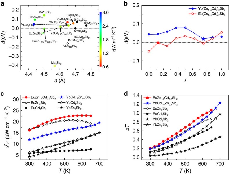
Figure 4a displays the Δ versus a compound map for CaAl2Si2-type Zintl compounds, where a is the lattice constant. The values of the thermal conductivity of reported Zintl compounds18,19,20,21,22,23,24,25,26,27,28,29,30,31,32,33 at 500 K are marked in the colour bar. Only a few compounds with band gaps smaller than 1.5 eV are illustrated out of the variety of Zintl compounds with CaAl2Si2-type structure. The compound maps as a function of, respectively, lattice constant a and band gap, with nearly all CaAl2Si2-type Zintl compounds are depicted in Supplementary Fig. 8a,b. In order to achieve an ideal Δ=0 value, one can select two or more compounds with positive (larger than 0) and negative (smaller than 0) Δ values and attempt to form a solid solution or mixture with Δ≈0 by slightly adjusting the molar ratio of the constituent compounds. This strategy constructs the overall picture of designing multinary CaAl2Si2-type Zintl compounds with ideal zero Δ values that yield good TE performance. Another possible optimizing approach is to select one compound with relatively low thermal conductivity and add it into one compound with nearly zero Δ forming a solid solution with the aim to block heat conduction without explicitly reducing the electronic transport through carefully tuning the molar ratio of the constituent compounds with poor heat conduction.
Figure 4. Solid solution map for designing high-performance multinary compounds with CaAl2Si2-type structure.
(a) Calculated Δ as a function of the lattice constant a in CaAl2Si2-type Zintl compounds with Eg<1.5 eV. The stars correspond to solid solutions YbCd1.5Zn0.5Sb2 and EuZn1.75Cd0.25Sb2 with nearly zero Δ values. Reported values18,19,20,21,22,23,24,25,26,27,28,29,30,31,32,33 of thermal conductivity at 500 K are shown in colour bar. (b) Calculated Δ versus the fraction x in two representative solid solutions Yb(Zn1–xCdx)2Sb2 and Eu(Zn1–xCdx)2Sb2. The stars represent solid solutions YbCd1.5Zn0.5Sb2 and EuZn1.75Cd0.25Sb2 with nearly zero Δ values. (c,d) Temperature dependence of power factors18,19 α2σ (c) and zT values18,19 (d) of YbZn2Sb2 (EuZn2Sb2), YbCd2Sb2 (EuCd2Sb2) and their solid solutions YbCd1.6Zn0.4Sb2 and EuZn1.8Cd0.2Sb2.
Through density functional theory calculation, Δ values as a function of the fraction x in two selected solid solutions Yb(Zn1−xCdx)2Sb2 and Eu(Zn1−xCdx)2Sb2 are simulated and shown in Fig. 4b. The results of Yb(Zn1−xCdx)2Sb2 and Eu(Zn1−xCdx)2Sb2 prove that it is indeed feasible to realize the ideal Δ value around zero in the selected solid solutions. The calculated band structure of an exemplified solid solution EuZn1.75Cd0.25Sb2 satisfying the nearly zero Δ value indicates that high orbital degeneracy at the valence band maxiamum is realized (Supplementary Fig. 9). Both Yb(Zn1−xCdx)2Sb2 and Eu(Zn1−xCdx)2Sb2 have been studied experimentally18,19. Figure 4c,d and Supplementary Fig. 10 show the temperature dependence of power factors, zT values, and thermal conductivities of two solid solutions YbCd1.6Zn0.4Sb2 and EuZn1.8Cd0.2Sb2 compared with the pure ternaries. The above two solid solutions with ideal Δ values around zero exhibit greatly enhanced power factors18,19 and zT values18,19 compared with non-alloyed compounds, consistent with the calculations. Moreover, the thermal conductivity of YbCd1.6Zn0.4Sb2 or EuZn1.8Cd0.2Sb2 is comparable to one of the constituent compounds. All the above results validate that the strategy based on solid solution maps is effective in the design of complex high-performance TE materials from a range of CaAl2Si2-type Zintl compounds. According to the well-established solid solution maps, there still exists many potential solid solutions that have not been reported yet, for example, Eu1−xCaxZn2Sb2, Yb1−xBaxMg2Sb2, Ca(Mg1−xCdx)2Sb2, Yb(Mg1−xZnx)2Sb2, Ca1−xBaxMg2Bi2 and so on. In particular, Ca(Zn1−xMgx)2Sb2, Sr1−xBaxMg2Sb2 and Sr(Mg1−xZnx)2Sb2 are promising TE candidates with earth-abundant, cheap and nontoxic chemical elements.
Biaxial strain engineering to optimize zT
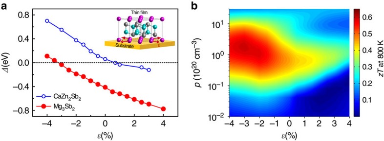
In addition to the solid solution method, external forces like biaxial strain can also be used to manipulate the Δ value. The biaxial strain can be introduced here by the lattice mismatch between the substrate materials with selected cubic lattice and the thin film TE materials with the CaAl2Si2-type structure deposited on the substrate. The biaxial strain ɛ can be defined as (a-a0)/a0 × 100%, where a0 and a are the in-plane lattice parameters with unstrained and strained states, respectively. Figure 5a shows Δ as a function of ɛ in two representative CaAl2Si2-type Zintl compounds, Mg3Sb2 and CaZn2Sb2. As the figure depicts, a linear correlation between Δ and ɛ is observed. The value of Δ increases (decreases) linearly with the increasing magnitude of the compressive (tensile) strain. Thus, we can deduce a general optimization rule for high TE performance, that is, for Zintl compounds with positive Δ value tensile biaxial strain is more effective, whereas for Zintl compounds with negative Δ value compressive biaxial strain is preferred. According to the first-principles calculations, the calculated power factors can be continuously tuned by biaxial strain and show peak values at optimal biaxial strains corresponding to nearly zero Δ values (Supplementary Fig. 11). For negative-Δ Mg3Sb2, the optimal biaxial strain turns out to be compressive, whereas for positive-Δ CaZn2Sb2, optimal biaxial strain appears to be tensile, fully consistent with the above deduction. Using semiclassical Boltzmann transport theory and experimental data30 (see Methods for details), the dependence of zT at 800 K on carrier concentration and biaxial strain is estimated for Mg3Sb2 and plotted in Fig. 5b. The maximum zT value of Mg3Sb2 at 800 K at the optimal strain −3% shows around 50% enhancement compared with the value of the unstrained case. Thus, biaxial strain engineering is an effective approach for tuning and optimizing TE performance, showing potential application to thin-film materials with the CaAl2Si2-type structure.
Figure 5. Biaxial strain engineering to optimize TE performance of CaAl2Si2-type Zintl compounds.
(a) Δ versus biaxial strain ɛ in two representative CaAl2Si2-type Zintl compounds Mg3Sb2 and CaZn2Sb2. Here biaxial strain ɛ is defined as (a−a0)/a0 × 100%, where a0 and a are the in-plane lattice parameters with unstrained and strained states, respectively. (b) The contour map of calculated zT value of Mg3Sb2 at 800 K as a function of hole concentration p and biaxial strain ɛ.
Extension of orbital engineering to several other compounds
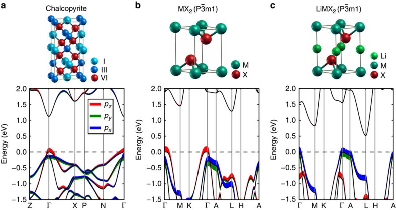
The orbital engineering approach based on zero-Δ screening rule, solid solution map and biaxial strain engineering developed here can also be used for optimizing a vast number of non-cubic compounds with similar p orbitals characteristics at the band edges. Figure 6 and Supplementary Figure 12 show the orbital-projected band structures and density of states of AgGaTe2, ZrS2 and LiZrSe2, which are representatives of chalcopyrites, metal dichalcogenides MX2 (space group: P m1) and lithium intercalated metal dichalcogenides LiMX2 (space group: P
 m1), respectively. All of these compounds possess crystal field split p orbital characteristics at the band edges, similar to the CaAl2Si2-type Zintl compounds. The results of biaxial strain engineering in chalcopyrites, metal dichalcogenides and lithium intercalated metal dichalcogenides from references (CuGaTe2 and TiS2)38,39 and our own data (ZrS2 and LiZrSe2; see Supplementary Fig. 13 for details) confirm orbital engineering. Detailed information including a solid solution map of metal dichalcogenides MX2 is provided in Supplementary Fig. 14 and Supplementary Table 3, with the aim to guide the optimization of p-type TE performance for metal dichalcogenides.
Figure 6. Extension of orbital engineering to several other non-cubic compounds.
(a–c) Orbital-projected band structures and crystal structures of representative chalcopyrite compound AgGaTe2 (a), metal dichalcogenide ZrS2 (b) and lithium intercalated metal dichalcogenide LiZrSe2 (c). px, py and pz orbitals of anions are projected on the band structures. Curve width indicates the relative weight of the component.
Discussion
In summary, we have proposed a novel approach to realize high orbital degeneracy at the band edges that yields good electronic transport properties and thereby high TE performance via tuning the relative energies of orbitals in layered CaAl2Si2-type Zintl compounds. We establish a simple yet insightful screening criterion: maintaining crystal field splitting energy around zero. Using the calculated Δ versus lattice parameter maps, one can conveniently choose two or more compounds to form a solid solution with the desirable zero Δ value that leads to excellent electronic transport performance. Moreover, Δ and TE performance can be continuously tuned and optimized by biaxial strain engineering.
Based on the orbital engineering approach, we predict a series of potential TE candidates with CaAl2Si2-type structure. Some of them have been proved experimentally with enhanced zT values. Several predicted promising compounds contain earth-abundant, cheap and nontoxic elements. Finally, the orbital engineering strategy is rationally extended to other types of materials with the same orbital features at the band edges. Thus, we believe that orbital engineering strategy based on zero-Δ rule and augmented by solid solution map and biaxial strain engineering opens a new avenue for high-throughput computational screening of TE materials and thereby will accelerate the screening and design of new high-performance TE materials from a myriad of non-cubic compounds.
Methods
Computational methods
Density Functional Theory calculations were carried out using the projector-augmented wave method40 as implemented in the Vienna ab initio simulation package41. HSE06 functional42 was used to relax the internal coordinates in the unit cell, whereas the lattice parameters of CaAl2Si2-type Zintl compounds were fixed to the experimental values from the literature. Here HSE06 functional was used to get structural parameters close to the experimental values. The plane-wave energy cutoff was set at 400 eV, and a 6 × 6 × 4 Monkhorst-Pack k mesh was used for crystal structure optimization. A 12 × 12 × 8 Monkhorst-Pack k mesh and a 32 × 32 × 18 Monkhorst-Pack k mesh were used for electronic structure calculations and transport properties calculations, respectively. An energy convergence criterion of 10−4 eV and a Hellmann-Feynman force convergence criterion of 0.008 eV Å−1 were adopted. Electronic structure calculations were implemented by combining the mBJ potential and the well-established PBE+U method43,44, and U=4 eV (ref. 44) was applied on Zn 3d states and Cd 4d states. This method has already been successfully applied to a wide range of narrow gap semiconductors to get accurate band gaps comparable to the experimental values43,44. Electrical transport property calculations were carried out by combining the ab initio band structure calculations and the Boltzmann transport theory under the constant carrier scattering time approximation as implemented in the BoltzTraP45 code. Calculation details of electronic structure for solid solutions, chalcopyrite (AgGaTe2), metal dichalcogenides and lithium intercalated metal dichalcogenide (LiZrSe2) are given in Supplementary Notes 3–5. The calculation methods here are enough to study materials discussed in this paper (Supplementary Fig. 15), but might be insufficient to be used to study strongly correlated materials such as Kondo Insulators46 with strong hybridization of localized f electrons with electronic bands.
To study the effects of biaxial strain, a variety of in-plane a lattice parameters were analysed, and for each of them, the c parameter and the atomic positions were optimized. The carrier relaxation time τ was reasonably assumed to be independent of the strain in current work as the crystal structure for each step tuned by the biaxial strain is rather small. The figure of merit zT of Mg3Sb2 under biaxial strain effect (Fig. 5b) was calculated using the following formula:
 |
Where α, σ/τ, and κe/τ can be directly obtained from BoltzTraP code. Thus, to obtain zT, we still need to know lattice thermal conductivity κL and constant scattering time τ. With the lattice thermal conductivity κL(330 K)=1.341 W m−1 K−1 of Mg3Sb2 obtained from ref. 30, κL(800 K)=0.553 W m−1 K−1 is estimated using the reciprocal relation of κL to T. Generally, under biaxial strain, lattice thermal conductivity is lower than that without strain because of the enhancement of phonon scattering by strain-induced defects47, which is beneficial to TE performance. To study the contribution to zT from electrical transport, lattice thermal conductivity here was assumed to be independent of biaxial strain. The carrier's scattering time τ could be derived from the relation μ=eτ/m*, where μ is the carrier mobility, m* is the effective mass of carrier and e is the elementary charge. Calculation details of constant carrier scattering time τ are provided in Supplementary Note 6 and Supplementary Table 4.
Additional information
How to cite this article: Zhang, J. et al. Designing high-performance layered thermoelectric materials through orbital engineering. Nat. Commun. 7:10892 doi: 10.1038/ncomms10892 (2016).
Supplementary Material
Supplementary Figures 1-15, Supplementary Tables 1-4, Supplementary Notes 1-6 and Supplementary References
Acknowledgments
We thank L. Chen, X. Liu, Y. Zhang and M. R. V. Jørgensen for discussions. This work was supported by the Danish National Research Foundation (DNRF93) and the Danish Center for Scientific Computing. X.S. acknowledges the support from the International S&T Cooperation Program of China (2015DFA51050) and Shanghai government (No. 15JC1400301 and 14DZ2261200). W.Z. acknowledges the support from the National Natural Science Foundation of China (Grant No. 11234012).
Footnotes
Author contributions J.Z. and B.B.I. designed the study. J.Z. and G.K.H.M. performed first-principles calculations. J.Z., L.S. and B.B.I. analysed data. K.F.F.F., W.Z. and X.S. provided discussions. J.Z. and B.B.I. wrote the manuscript and all authors edited the manuscript.
References
- Snyder G. J. & Toberer E. S. Complex thermoelectric materials. Nat. Mater 7, 105–114 (2008). [DOI] [PubMed] [Google Scholar]
- Nolas G. S., Sharp J. & Goldsmid H. J. Thermoelectrics: Basic Principles and New Materials Developments Springer (2001). [Google Scholar]
- Snyder G. J., Christensen M., Nishibori E., Caillat T. & Iversen B. B. Disordered zinc in Zn4Sb3 with phonon-glass and electron-crystal thermoelectric properties. Nat. Mater 3, 458–463 (2004). [DOI] [PubMed] [Google Scholar]
- Hsu K. F. et al. Cubic AgPbmSbTe2+m: Bulk thermoelectric materials with high figure of merit. Science 303, 818–821 (2004). [DOI] [PubMed] [Google Scholar]
- Pei Y. et al. Convergence of electronic bands for high performance bulk thermoelectrics. Nature 473, 66–69 (2011). [DOI] [PubMed] [Google Scholar]
- Heremans J. P. et al. Enhancement of thermoelectric efficiency in PbTe by distortion of the electronic density of states. Science 321, 554–557 (2008). [DOI] [PubMed] [Google Scholar]
- Liu H. L. et al. Copper ion liquid-like thermoelectrics. Nat. Mater 11, 422–425 (2012). [DOI] [PubMed] [Google Scholar]
- Hochbaum A. I. et al. Enhanced thermoelectric performance of rough silicon nanowires. Nature 451, 163–167 (2008). [DOI] [PubMed] [Google Scholar]
- Sales B. C., Mandrus D. & Williams R. K. Filled skutterudite antimonides: A new class of thermoelectric materials. Science 272, 1325–1328 (1996). [DOI] [PubMed] [Google Scholar]
- Biswas K. et al. High-performance bulk thermoelectrics with all-scale hierarchical architectures. Nature 489, 414–418 (2012). [DOI] [PubMed] [Google Scholar]
- Christensen M. et al. Avoided crossing of rattler modes in thermoelectric materials. Nat. Mater 7, 811–815 (2008). [DOI] [PubMed] [Google Scholar]
- Madsen G. K. H. Automated search for new thermoelectric materials: the case of LiZnSb. J. Am. Chem. Soc. 128, 12140–12146 (2006). [DOI] [PubMed] [Google Scholar]
- Yang J. et al. Evaluation of half-Heusler compounds as thermoelectric materials based on the calculated electrical transport properties. Adv. Funct. Mater. 18, 2880–2888 (2008). [Google Scholar]
- Zaitsev V. K. et al. Highly effective Mg2Si1−xSnx thermoelectrics. Phys. Rev. B 74, 045207 (2006). [Google Scholar]
- Liu W. et al. Convergence of conduction bands as a means of enhancing thermoelectric performance of n-type Mg2Si1-xSnx solid solutions. Phys. Rev. Lett. 108, 166601 (2012). [DOI] [PubMed] [Google Scholar]
- Zhang J. et al. High-performance pseudocubic thermoelectric materials from non-cubic chalcopyrite compounds. Adv. Mater. 26, 3848–3853 (2014). [DOI] [PubMed] [Google Scholar]
- Bhattacharya S. & Madsen G. K. H. High-throughput exploration of alloying as design strategy for thermoelectrics. Phys. Rev. B 92, 085205 (2015). [Google Scholar]
- Wang X.-J. et al. Synthesis and high thermoelectric efficiency of Zintl phase YbCd2−xZnxSb2. Appl. Phys. Lett. 94, 092106 (2009). [Google Scholar]
- Zhang H. et al. Thermoelectric properties of Eu(Zn1-xCdx)2Sb2. Dalton Trans. 39, 1101–1104 (2010). [DOI] [PubMed] [Google Scholar]
- Guo K. et al. Enhanced thermoelectric figure of merit of Zintl Phase YbCd2-xMnxSb2 by chemical substitution. Eur. J. Inorg. Chem. 2011, 4043–4048 (2011). [Google Scholar]
- Cao Q.-G. et al. Zintl phase Yb1-xCaxCd2Sb2 with tunable thermoelectric properties induced by cation substitution. J. Appl. Phys. 107, 053714 (2010). [Google Scholar]
- Zhang H. et al. Synthesis and properties of CaCd2Sb2 and EuCd2Sb2. Intermetallics 18, 193–198 (2010). [Google Scholar]
- Zevalkink A. et al. Nonstoichiometry in the Zintl phase Yb1−δZn2Sb2 as a route to thermoelectric optimization. Chem. Mater. 26, 5710–5717 (2014). [Google Scholar]
- Condron C. L., Kauzlarich S. M., Gascoin F. & Snyder G. J. Thermoelectric properties and microstructure of Mg3Sb2. J. Solid State Chem. 179, 2252–2257 (2006). [Google Scholar]
- Stark D. & Snyder G. J. in Proc. 21th Inter. Conf. Thermoelectrics 181–184Long Beach, CA, USA (2002). [Google Scholar]
- Zhang H. et al. A new type of thermoelectric material, EuZn2Sb2. J. Chem. Phys. 129, 164713 (2008). [DOI] [PubMed] [Google Scholar]
- Gascoin F., Ottensmann S., Stark D., Haïle S. M. & Snyder G. J. Zintl phases as thermoelectric materials: tuned transport properties of the compounds CaxYb1-xZn2Sb2. Adv. Funct. Mater. 15, 1860–1864 (2005). [Google Scholar]
- May A. F. et al. Thermoelectric transport properties of CaMg2Bi2, EuMg2Bi2, and YbMg2Bi2. Phys. Rev. B 85, 035202 (2012). [Google Scholar]
- Toberer E. S., May A. F., Melot B. C., Flage-Larsen E. & Snyder G. J. Electronic structure and transport in thermoelectric compounds AZn2Sb2 (A=Sr, Ca, Yb, Eu). Dalton Trans. 39, 1046–1054 (2010). [DOI] [PubMed] [Google Scholar]
- Bhardwaj A. et al. Mg3Sb2-based Zintl compound: a non-toxic, inexpensive and abundant thermoelectric material for power generation. RSC Adv 3, 8504–8516 (2013). [Google Scholar]
- Zhang H. et al. Thermoelectric properties of YbxEu1-xCd2Sb2. J. Chem. Phys. 133, 194701 (2010). [DOI] [PubMed] [Google Scholar]
- Zhang H. et al. Thermoelectric properties of polycrystalline SrZn2Sb2 prepared by spark plasma sintering. J. Electron. Mater. 39, 1772–1776 (2010). [Google Scholar]
- Ponnambalam V. & Morelli D. On the thermoelectric properties of Zintl compounds Mg3Bi2-xPnx (Pn=P and Sb). J. Electron. Mater. 42, 1307–1312 (2013). [Google Scholar]
- Zheng C., Hoffmann R., Nesper R. & Von Schnering H. G. Site preferences and bond length differences in CaAl2Si2-type Zintl compounds. J. Am. Chem. Soc. 108, 1876–1884 (1986). [Google Scholar]
- Toberer E. S., May A. F. & Snyder G. J. Zintl chemistry for designing high efficiency thermoelectric materials. Chem. Mater. 22, 624–634 (2010). [Google Scholar]
- Bjerg L., Madsen G. K. H. & Iversen B. B. Ab initio calculation of intrinsic point defects in ZnSb. Chem. Mater. 24, 2111–2116 (2012). [Google Scholar]
- Kim S. et al. Thermoelectric properties of Mn-doped Mg-Sb single crystals. J. Mater. Chem. A 2, 12311–12316 (2014). [Google Scholar]
- Samanta A., Pandey T. & Singh A. K. Strain-induced electronic phase transition and strong enhancement of thermopower of TiS2. Phys. Rev. B 90, 174301 (2014). [Google Scholar]
- Xue L., Xu B., Zhao D. & Yi L. First-principles prediction the effect of lattice deformation on thermoelectric properties of CuGaTe2. Comput. Mater. Sci. 90, 143–147 (2014). [Google Scholar]
- Blöchl P. E. Projector augmented-wave method. Phys. Rev. B 50, 17953–17979 (1994). [DOI] [PubMed] [Google Scholar]
- Kresse G. & Furthmüller J. Efficient iterative schemes for ab initio total-energy calculations using a plane-wave basis set. Phys. Rev. B 54, 11169–11186 (1996). [DOI] [PubMed] [Google Scholar]
- Paier J. et al. Screened hybrid density functionals applied to solids. J. Chem. Phys. 124, 154709 (2006). [DOI] [PubMed] [Google Scholar]
- Tran F. & Blaha P. Accurate band gaps of semiconductors and insulators with a semilocal exchange-correlation potential. Phys. Rev. Lett. 102, 226401 (2009). [DOI] [PubMed] [Google Scholar]
- Zhang Y. et al. Near-edge band structures and band gaps of Cu-based semiconductors predicted by the modified Becke-Johnson potential plus an on-site Coulomb U. J. Chem. Phys. 139, 184706 (2013). [DOI] [PubMed] [Google Scholar]
- Madsen G. K. H. & Singh D. J. BoltzTraP. A code for calculating band-structure dependent quantities. Comput. Phys. Commun. 175, 67–71 (2006). [Google Scholar]
- Hong S., Ghaemi P., Moore J. E. & Phillips P. W. Tuning thermoelectric power factor by crystal-field and spin-orbit couplings in Kondo-lattice materials. Phys. Rev. B 88, 075118 (2013). [Google Scholar]
- Wiedigen S. et al. Interplay of point defects, biaxial strain, and thermal conductivity in homoepitaxial SrTiO3 thin films. Appl. Phys. Lett. 100, 061904 (2012). [Google Scholar]
Associated Data
This section collects any data citations, data availability statements, or supplementary materials included in this article.
Supplementary Materials
Supplementary Figures 1-15, Supplementary Tables 1-4, Supplementary Notes 1-6 and Supplementary References


